Electromigration in thin tunnel junctions with ferromagnetic/nonmagnetic: nanoconstrictions, local heating, and direct and wind forces
Abstract
Current Induced Resistance Switching (CIS) was recently observed in thin tunnel junctions with ferromagnetic (FM) electrodes i.e FM/I/FM. This effect was attributed to electromigration of metallic atoms in nanoconstrictions in the insulating barrier (I). Here we study how the CIS effect is influenced by a thin non-magnetic (NM) Ta layer, deposited just below the AlOx insulating barrier in tunnel junctions of the type FM/NM/I/FM (FM=CoFe). Enhanced resistance switching occurs with increasing maximum applied current (), until a plateau of constant CIS is reached for mA (CIS60%) and above. However, such high electrical currents also lead to a large (9%) irreversible resistance decrease, indicating barrier degradation. Anomalous voltage-current characteristics with negative derivative were also observed near and this effect is here attributed to heating in the tunnel junction. One observes that the current direction for which resistance switches in FM/NM/I/FM (clockwise) is opposite to that of FM/I/FM tunnel junctions (anti-clockwise). This effect will be discussed in terms of a competition between the electromigration contributions due to the so called direct and wind forces. It will be shown that the direct force is likely to dominate electromigration in the Ta (NM) layers, while the wind contribution likely dominates in the CoFe (FM) layers.
pacs:
66.30.Pa, 66.30.Qa, 73.40.Gk, 73.40.Rw, 85.75.DdI Introduction
Tunnel junctions (TJ) consisting of two ferromagnetic (FM) layers separated by an insulator (I) Moodera et al. (1995) show enormous potential for a multiplicity of applications such as read head,Song et al. (2000) strain,Lohndorf et al. (2002) current, position and speed Freitas et al. (2000) sensors or even to detect magnetically tagged biological specimens.Ferreira et al. (2003) However, probably the most sought after application is high performance, low cost, non-volatile magnetoresistive random access memories (MRAMs).Tehrani et al. (2000) In a tunnel junction, the magnetization of one of the FM layers (pinned layer) is fixed by an underlying antiferromagnetic (AFM) layer. The magnetization of the other FM layer (free layer) reverses almost freely when a small magnetic field is applied. Due to spin dependent tunneling Meservey and Tedrow (1994) one obtains two distinct resistance (R) states corresponding to pinned and free layer magnetizations parallel (low R) or antiparallel (high R). However, several drawbacks are still of concern in actual MRAM submicron devices, like cross-talk in the array configuration or the large power consumption to generate the magnetic field to switch R. One then aims to replace the magnetic field-driven magnetization reversal by a Current Induced Magnetization Switching (CIMS) mechanism.Slonczewski (1996); Berger (1996) Such goal was recently achieved in magnetic tunnel junctions Huai et al. (2004); Fuchs et al. (2004) for current densities A/cm2. On the other hand, Liu et al. Liu et al. (2003a) observed reversible resistance changes induced by lower current densities ( A/cm2) in thin FM/I/FM TJs. These changes, although initially attributed to the CIMS mechanism, were later found Liu et al. (2003b) not dependent on the relative orientation of the magnetizations of the free and pinned layers. This effect was then called Current Induced Switching (CIS) and is now attributed Deac et al. (2004); Ventura et al. (2005a) to electromigration (EM) in nanoconstrictions in the insulating barrier. The combination of the tunnel magnetoresistive and CIS effects allows the use of a magnetic tunnel junction as a three resistance state device.Ventura et al. (2005b) Both CIS and CIMS effects seem to coexist in thin magnetic tunnel junctions for A/cm2. The reasons for the observed dominance of one effect over the other are still unclear but likely related to structural differences in the tunnel junctions. One notes however, that electromigration can in fact limit the implementation of the spin torque mechanism in actual devices and be a major reliability issue in read head sensors.Bae et al. (2002)
When a metal is subjected to an electrical field E, the usual random diffusive motion of atoms is biased by the resulting driving force F, and a net atomic flux can be observed. This phenomena is known as electromigration Sorbello (1998) and F can be written as:
| (1) |
where is the effective valence and is the elementary charge. The force acting on the migrating ion is usually separated into two components, both linear in the external applied electrical field:
| (2) |
The direct force arises from the electrostatic interactions between the electrical field and the so called direct valence of the ion (). The theoretical calculation of the direct force is a challenging process but (ion valence) is usually assumed. The wind force results from momentum exchange between the current carrying electrons and the migrating ions and so it has the direction of the electron current (opposite to the electrical field). The wind valence is simply a convenient term to describe the wind force, arising from the fact that is proportional to the current density and, in an ohmic material, to E. The competition between wind and direct forces is often dominated by the first, which usually controls the sign and magnitude of the effective valence and the EM process.
Here we study how a Ta non-magnetic (NM) amorphous thin layer deposited just below the insulating barrier influences the Current Induced Switching. In a CIS cycle, the resistance commutes between two states due to electromigration of ions from the electrodes into the barrier (decreasing R) and from the barrier back into the electrodes (increasing R).Deac et al. (2004) We can then define the CIS coefficient as the relative difference between these two R-states. Interestingly, the current direction for which R-switching occurs in FM/NM/I/FM tunnel junctions is opposite to that of FM/I/FM tunnel junctions.Ventura et al. (2005a) Using the intuitive ballistic model of EM, we will show that the direct force is likely to dominate electromigration in Ta (NM) layers, while the wind force dominates in CoFe (FM) layers. The switching direction difference will be here associated with the dominance of different EM forces (direct or wind) in the two types of tunnel junctions referred.
The CIS coefficient was strongly enhanced by increasing the maximum applied current (), reaching almost 60% for mA. However, severe R-degradation occurs when mA. Voltage-current characteristics show strong anomalous non-linearities, here associated with heating effects. Comparing our experimental results with voltage-current characteristics as predicted by Simmons’ model,Simmons (1963) we estimate that the temperature inside the tunnel junction reaches 600 K for mA. Numerical results from a model of heat generation in tunnel junctions suggest that such high temperatures can only occur if local current densities much larger than ( the electrical current and the total tunnel junction area) exist within the barrier. One concludes that these hot-spots concentrate most of the current flowing through the tunnel junction stack and are likely the reason for the occurrence of EM in the studied tunnel junctions.
II Electromigration
For atomic diffusion to occur, an atom needs to surmount the energy barrier separating neighboring equilibrium lattice sites (Fig. 1a). When an electric current flows through a metal this usual, thermally-activated, random motion of atoms is biased by the electrical field (Fig. 1b), resulting in a net atomic flow. This phenomena is know as electromigration Sorbello (1998) and is currently the major cause of failure of interconnects in integrated circuits.Ogawa et al. (2002) Studies of EM in interconnects are performed under severe conditions, such as high electrical current densities ( A/cm2) and temperature (– K) and show that EM can occur through different diffusion paths, such as grain boundary and interfaces, as in Al Liu et al. (1999) and Cu Gan et al. (2001) interconnects, respectively. The relative importance of the different diffusion paths varies with the material properties, such as grain size and orientation, interface bonding and structure.

Electromigration is also a concern in magnetic nanostructures, namely spin valves and tunnel junctions.Bae et al. (2002) During device operation, local structural inhomogeneities can lead to large current density, and thus to electromigration. This is of particular importance in tunnel junctions where the resistance depends exponentially on the barrier thickness and where localized nanoconstrictions can concentrate most of the current. Such high current densities can also produce intense heating leading to enhanced electromigration.Bae et al. (2002) Discrete electromigration events were observed in metallic nanobridges (for A/cm2).Ralls et al. (1989) Reversible EM was recently observed in Ni nanoconstrictions ( A/cm2) Céspedes et al. (2003) and thin tunnel junctions ( A/cm2).Liu et al. (2003a); Deac et al. (2004) Electromigration in these nanostructures can lead to both an increase and a decrease of the electrical resistance, depending on the sense of the applied electrical current, and thus on the sense of EM-driven atomic motion.
The ballistic model of electromigration presents the most intuitive picture of the underlying physics of EM. The wind force is calculated assuming that all the momentum lost by the scattered electrons is transferred to the migrating ion.Ralls et al. (1989) In the free electron approximation the wind valence becomes:Sorbello (1998)
| (3) |
where is the electron density, is the electron mean free path and is the electron transport cross section for scattering by the ion. Using, e.g. known values for Fe ( Å-3, Å, Å2),Ashcroft and Mermin (1976); Bly and Rous (1996) one finds (). Such estimative confirms that the wind force usually dominates electromigration. More elaborated EM models such as the pseudopotential method give lower values, by as much as 70%.Sorbello (1998) However, because of its simplicity, we will use the ballistic model to qualitatively explain our results.
Sorbello Sorbello (1989) first studied electromigration forces in mesoscopic systems. In particular he considered electromigration near a point contact, modeled as a circular aperture of radius between two metallic layers of electrical resistivity . He found that the direct force is then greatly enhanced near such constriction. An estimate on the relative magnitude of the wind and direct forces gives:Sorbello (1989); Ralls et al. (1989)
| (4) |
which evidences the important role played by the constriction geometry: the smaller the constriction radius, the larger will be the direct force compared to the wind force.
III Experimental details
In this work we used a series of ion beam deposited tunnel junctions, with a non-magnetic Ta layer inserted just below the insulating AlOx barrier. The complete structure of the tunnel junctions studied was glass/bottom lead/Ta (90 Å)/NiFe (50 Å)/MnIr (90 Å)/CoFe (40 Å)/Ta (20 Å)/AlOx (3 Å+ 4 Å)/CoFe (30 Å)/NiFe (40 Å)/Ta (30 Å)/TiW(N) (150 Å)/top lead. The chosen structure is similar to that of magnetic tunnel junctions grown for actual applications except for the additional Ta layer, thus making a comparison between the FM/I/FM and FM/NM/I/FM systems easier. Previous Transmission Electron Microscopy images obtained in similar samples show no significant microstructural changes induced by a Ta layer deposited below the barrier.Kyung et al. (2002) The AlOx barrier was formed by two-step deposition and natural oxidation processes (50 mTorr, 3 min, 100 mTorr, 20 min).Liu et al. (2003a) NiFe, CoFe, MnIr and TiW(N) stand for Ni80Fe20, Co80Fe20 and Mn78Ir22, Ti10W90(N). The bottom and top leads are made of Al 98.5% Si 1% Cu 0.5%, and are 600 Å (26 m) and 3000 Å (10 m) thick (wide) respectively. The junctions were patterned to a rectangular shape with area m2 by a self-aligned microfabrication process.
The electrical resistance, magnetoresistance and current induced switching were measured with a four-point d.c. method, with a current stable to 1:106 and using an automatic control and data acquisition system.
CIS cycles were performed using the pulsed current method Liu et al. (2003b) allowing us to measure the remnant resistance of the tunnel junction after each current pulse. Current pulses () of 1 s duration and 5 s repetition period are applied to the junction, starting with increasing negative pulses from (where we define the resistance as ), in mA steps up to a maximum , dependent on cycle in the 10–80 mA range. One then decreases the current pulses (always with the same ), following the reverse trend through zero current pulse () down to negative , and then again to zero (), closing the CIS hysteretic cycle, . Positive current is here defined as flowing from the bottom to the top lead.
The junction remnant resistance is measured in the 5 s-waiting periods between consecutive current pulses, using a low current of 0.1 mA, providing a curve for each cycle. This low current method allows us to systematically discard non-linear I(V) contributions to the resistance. However, the voltage across the TJ is also measured while applying the current pulse , enabling us to obtain the (non-linear) V() characteristic for each CIS cycle.
Using the definitions above, one can define the CIS coefficient as:
| (5) |
We also define the resistance shift () in each cycle:
| (6) |
IV Experimental results
The studied tunnel junction had an initial electrical resistance and a resistance area product m2. No magnetoresistance was observed in our tunnel junctions, due to the loss of interfacial polarization (20 Å Ta layer deposited just below the barrier). In fact, the tunnel magnetoresistance of a TJ is known to exponentially decrease with the thickness of a non-magnetic layer inserted just below the insulating barrierLeclair et al. (2000); Kyung et al. (2002) and TMR then goes rapidly to zero within the first monolayers of the non-magnetic material.
We measured CIS cycles with increasing , starting with a cycle up to mA (Fig. 2a; cycle starting at point S) giving % and %. No resistance switching was observed under the initial negative current pulses (). However, upon reversing the current one observes that for mA (where we define the positive critical current ; see Fig. 2a) the resistance starts to decrease, a trend which becomes increasingly enhanced (switching) with , up to mA. This switching is associated with electromigration of metallic ions from the electrodes into the barrier,Deac et al. (2004); Ventura et al. (2005a) decreasing the effective barrier thickness and consequently the junction resistance. The previous absence of R-switching under negative current pulses indicates an electromigration asymmetry with respect to the electrode/oxide interfaces, i.e. only ions from one such interface are actively participating in electromigration. Physically such asymmetry arises not only from the different materials deposited just below (Ta) and above (CoFe) the insulating barrier, but also from the deposition and oxidation processes during tunnel junction fabrication. In particular the top electrode is deposited over an oxidized smooth surface, while a much more irregular bottom electrode/oxide interface is experimentally observed.Wang et al. (2003) Since the migration of ions into and out of the barrier should occur preferentially in nanoconstrictions (higher electrical fields), one concludes that such ions likely belong to the Ta bottom electrode. The current density and electrical field at R-switching can be estimated as A/cm2 and MV/cm, respectively.
Returning to Fig. 2a, the subsequent decrease of from to zero hardly affects the low resistance state. However, for mA (where we define the negative critical current ), the resistance gradually increases until , recovering a significant fraction of the previous R-switching near . This indicates that, under a reversed electrical field, many ions return to their initial sites. The subsequent change of from to zero (to close the CIS cycle at point F) produces no significant change in resistance. However, the final resistance mismatch (; %) indicates some irreversible effects in this CIS cycle ( mA), associated with barrier degradation.

The voltage across the junction was also measured for each applied current pulse (), providing the V() characteristic depicted in Fig. 2b (hollow circles). If one uses Simmons’ model Simmons (1963) to fit this curve with adequate thin TJ barrier parameters Deac et al. (2004) (barrier thickness Å, barrier height eV), the quality of the fit is poor (dashed line in Fig. 2b), with large discrepancies near . Also, the use of the Brinkman model for asymmetric tunnel junctions Brinkman et al. (1970) does not yield good fits. Such discrepancies near are related to localized heating inside the tunnel junction, as discussed below.
We then performed CIS cycles with increasing , from 30 to 80 mA, in mA steps as shown for representative cycles in Fig. 3. Notice the enhanced R-switching and R-recovering stages (versus ), occurring from to and from to respectively. From these data one can obtain the CIS and -shift in each cycle, obtaining the corresponding dependence on as depicted in Fig. 4. The CIS coefficient rises with until 65 mA (%), saturating for higher current pulses. On the other hand, remains fairly small below mA (-0.4%), but increases rapidly for higher ( for mA). The CIS increase with indicates that electromigrated ions are further pushed into the barrier (further lowering R) or/and more ions participate in the EM processes. Ultimately irreversible damage occurs in the barrier, as reflected in the -shift enhancement for mA (Fig. 4).


V Discussion
The observed resistance switching (R decrease) occurs only for positive current pulses in the here studied FM/NM/I/FM tunnel junctions (R-recovery occurs under negative ; see Figs. 2a, 3 and 5), whereas in the previously studied FM/I/FM Ventura et al. (2005a) tunnel junctions switching (recovery) occurs under negative (positive) currents (Fig. 5b; ). To explain such different behavior one will compare electromigration direct and wind forces in Ta (NM) and CoFe (FM) layers. Using eq. 3 we obtain:
| (7) |
where is the Fermi velocity. Inserting the parameters given in Table 1 Ashcroft and Mermin (1976); Bly and Rous (1996); Chakraborty et al. (1976); Gehanno et al. (1999) one obtains . The wind force is then much larger in CoFe than in Ta layers and likely dominates electromigration in the CoFe layers. On the contrary, because Ta is in an amorphous state (notice its high electrical resistivity in Table 1), one expects the small electron mean free path to prevent large momentum gains by electrons between consecutive collisions. Using the value estimated previously for , one finds (). Remembering that the magnitude of the direct force is enhanced relatively to the wind force in nanoconstrictions (eq. 4; see also below) and that the ballistic model overestimates , one expects the direct force to dominate in Ta. Thus, the likely cause for the observed difference in the R-switching directions is related to the dominance of different electromigration forces in Ta and CoFe. Confirming this conclusion, tunnel junctions with Ta layers deposited just below and just above the insulating barrier (FM/NM/I/NM/FM; not shown) display the same current switching direction as those with only one Ta layer below the insulating barrier (FM/NM/I/FM). On the other hand, when a single NM Ta layer is deposited just above the barrier (FM/I/NM/FM), the R-switching direction is that of FM/I/FM tunnel junctions.

| () Gehanno et al. (1999) | (Å2) Bly and Rous (1996) | (cm/s) Ashcroft and Mermin (1976); Chakraborty et al. (1976) | |
|---|---|---|---|
| CoFe | 17.1 | 3 | 2 |
| Ta | 154.0 | 6 | 0.67 |
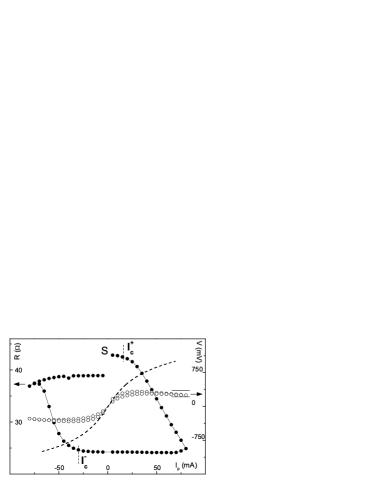
Figure 6 (left scale) shows the CIS R()-cycle obtained at room temperature, with mA (%; %). Notice the R()-switching from mA to mA and resistance recovery from mA to - mA. The V() characteristic is also displayed (hollow circles; right scale), showing an anomalous plateau with a slight dV/d negative slope for | mA. This effect cannot be explained by tunnel transport theories and is here related to heating inside the tunnel junction. Using our temperature dependent R-data,Ventura et al. (2005c) the temperature inside the tunnel junction is estimated as 600 K. Such high temperatures have also been observed in similar measurements performed in FM/I/FM tunnel junctions.Ventura et al. (2005a)
Heat generation in tunnel junctions arises from two processes:Sousa et al. (2004) usual Joule heating in the metallic layers and inelastic electron scattering upon ballistic tunneling. The steady-state heat equation can then be written as:Sousa et al. (2004)
| (8) |
where is the heat conductivity, is the temperature, is the stack position, is the current density, is the bias voltage and is the inelastic scattering electron mean free path. We obtained numerical results assuming that the current density is constant throughout the junction stack. The temperature at the bottom and top of the tunnel junction stack is assumed fixed at 300 K.
Our numerical results (Fig. 7) indicate that large heating can occur near the insulating barrier for high current densities. However, the temperature increase expected from the uniform case, A/cm2 is negligible ( K; inset of Fig. 7), and to reach K one needs A/cm2. This corresponds to an effective area through which current flows m2, i.e., about 2.5% of the total tunnel junction area. These results then suggest that is only an average value and that nanoconstrictions where the insulating barrier is thinner concentrate most of the current flowing through the junction. Such hot-spots have been observed in similar TJs by atomic force microscopy.Sousa et al. (2004)

One can now understand the observed electromigration driven resistance changes in thin FM/NM/I/FM tunnel junctions with NM=Ta (amorphous; Fig. 5a). Under increasing positive current pulses (directed from the bottom to the top lead), the dominating EM direct force induced by the electrical field pushes Ta atoms into the barrier, a process thermally assisted by heating generated by the high current densities flowing in nanoconstrictions. This rises the probability that an atom surmounts the energy barrier for migration (see Fig. 1), greatly enhancing atomic mobility. One notices that even a small barrier weakening (due to such migration) would considerably lower the tunnel resistance due to its exponential dependence on barrier thickness.Simmons (1963) Using the Simmons’ model we can calculate the resistance variation due to a small barrier thickness reduction from to ():
| (9) |
where . For a CIS coefficient of % one obtains a barrier thickness decrease Å. We can now plot the magnitude of the expected decrease as a function of the maximum applied current (Fig. 8; using the experimental and values), which follows the same trend as the CIS coefficient (Fig. 3). In particular, a non-linear behavior (apparently exponential, as more clearly visible at low temperatures Ventura et al. (2005c)) is observed for mA, that is, while the -shift is small and electromigration is mainly reversible. In atomic diffusion processes one often has Ghez (1988) ( the position and the time). Therefore, in electromigration , i.e. the barrier thickness decrease is proportional to the applied electrical field density and to the migration time . Following this simple analysis, one has . The CIS effect then depends on how local electrical fields behave near nanoconstrictions and on its dependence on nanostructural atomic rearrangements.

Time dependent measurements (over 4 h) revealed that R remains practically constant both in its high and low state (not shown). This indicates that under a reduced driving force, displaced Ta ions remain trapped in deep enough local energy minima inside lattice potential barriers (), so that thermal fluctuations cannot return them to the electrodes. For example, in the CIS cycle of Fig. 5a one observes that the low resistance state persists for current pulses from down to . However, when the driving force gets strong enough to return displaced ions back into their initial positions in the NM layer. However, the final resistance does not exactly reaches its initial value, indicating progressive barrier degradation. Such degradation should result from metallic ions that remain in the barrier after the CIS cycle is completed. We also notice that in the initial CIS cycle with mA (Fig. 5a) one has . This indicates that the driving force for electromigration into and out of the insulating barrier is approximately equal, i.e. the lattice sites where ions migrate to are energetically similar. Furthermore, Fig. 3 (see dashed line) shows that mA throughout all the CIS cycles performed, indicating that cycling does not alter the EM force inducing atomic migration from Ta into the barrier. In other words, the energy barrier which the Ta ions surmount when migrating into the barrier is kept constant (inset of Fig. 8). This contrasts with electromigration in the opposite direction, where increases with cycling (Fig. 3; see dotted line). The force needed to return ions back has to be increased (inset of Fig. 8), indicating that Ta ions migrating under increasingly higher current pulses are pushed further inside the barrier, and are thus more difficult to return to the electrode.
VI Conclusions
We studied the Current Induced Switching effect on low resistance (7 Å barrier) CoFe/Ta/AlO/CoFe tunnel junctions. The CIS coefficient increased with increasing maximum applied current pulses, reaching 60% for mA. Such effect is controlled by nanostructural rearrangements at the electrodes/barrier interfaces, due to ion electromigration (reversible and irreversible). When high currents are applied, one observes large irreversible resistance decreases. The V() characteristics showed an anomalous behavior when mA due to heating effects inside the tunnel junction, showing that the CIS effect is thermally assisted. The analysis of these effects shows that nanoconstrictions indeed concentrate most of the tunneling current through the barrier, forming local hot-spots. One further demonstrates that the R-switching direction is related to a competition between the electromigration contributions due to direct and wind forces: the direct force dominates electromigration in Ta layers, whereas the wind contribution is dominant in CoFe.
Finally, please notice that, although the results presented here concern a single FM/NM/I/FM tunnel junction, they are reproduced when measuring other TJs from the same deposition batch. Particularly, the dependence of the CIS coefficient on maximum applied electrical current is quite similar in different tunnel junctions. The current switching direction is always the same for the same TJ-structure.
Acknowledgements.
Work supported in part by FEDER-POCTI/0155, POCTI/CTM/36489/2000, POCTI/CTM/45252/02 and POCTI/CTM/59318/2004 from FCT and IST-2001-37334 NEXT MRAM projects. J. Ventura is thankful for a FCT doctoral grant (SFRH/BD/7028/2001). Z. Zhang and Y. Liu are thankful for FCT post-doctoral grants (SFRH/BPD/1520/2000 and SFRH/BPD/9942/2002).References
- Moodera et al. (1995) J. S. Moodera, L. R. Kinder, T. M. Wong, and R. Meservey, Phys. Rev. Lett. 74, 3273 (1995).
- Song et al. (2000) D. Song, J. Nowak, R. Larson, P. Kolbo, and C. R., IEEE Trans. Magn. 36, 2545 (2000).
- Lohndorf et al. (2002) M. Lohndorf, T. Duenas, M. Tewes, E. Quandt, M. Ruhrig, and J. Wecker, Appl. Phys. Lett. 81, 313 (2002).
- Freitas et al. (2000) P. P. Freitas, F. Silva, N. J. Oliveira, L. V. Melo, L. Costa, and N. Almeida, Sensors and Actuators A - Physical 81, 2 (2000).
- Ferreira et al. (2003) H. A. Ferreira, D. L. Graham, P. P. Freitas, and J. M. S. Cabral, J. Appl. Phys. 93, 7281 (2003).
- Tehrani et al. (2000) S. Tehrani, B. Engel, J. M. Slaughter, E. Chen, M. DeHerrera, M. Durlam, P. Naji, R. Whig, J. Janesky, and J. Calder, IEEE Trans. Magn. 36, 2752 (2000).
- Meservey and Tedrow (1994) R. Meservey and P. M. Tedrow, Phys. Rep. 238, 173 (1994).
- Slonczewski (1996) J. C. Slonczewski, J. Magn. Magn. Mater. 159, L1 (1996).
- Berger (1996) L. Berger, Phys. Rev. B 54, 9353 (1996).
- Huai et al. (2004) Y. Huai, F. Albert, P. Nguyen, M. Pakala, and T. Valet, Appl. Phys. Lett. 84, 3118 (2004).
- Fuchs et al. (2004) G. D. Fuchs, N. C. Emley, I. Krivoritov, P. Braganca, E. M. Ryan, S. Kiselev, J. Sankey, D. C. Ralph, R. A. Buhrman, and J. A. Katine, Appl. Phys. Lett. 85, 1205 (2004).
- Liu et al. (2003a) Y. Liu, Z. Zhang, P. P. Freitas, and J. L. Martins, Appl. Phys. Lett. 82, 2871 (2003a).
- Liu et al. (2003b) Y. Liu, Z. Zhang, and P. P. Freitas, IEEE Trans. Magn. 39, 2833 (2003b).
- Deac et al. (2004) A. Deac, O. Redon, R. C. Sousa, B. Dieny, J. P. Nozières, Z. Zhang, Y. Liu, and P. P. Freitas, J. Appl. Phys. 95, 6792 (2004).
- Ventura et al. (2005a) J. Ventura, J. Araujo, J. B. Sousa, Y. Liu, Z. Zhang, and P. P. Freitas (2005a), submitted to IEEE Trans. Nanotechnol.
- Ventura et al. (2005b) J. Ventura, J. Araujo, J. B. Sousa, Y. Liu, Z. Zhang, and P. P. Freitas (2005b), submitted to Appl. Phys. Lett.
- Bae et al. (2002) S. Bae, I. F. Tsu, M. Davis, E. S. Murdock, and J. H. Judy, IEEE Trans. Magn. 38, 2655 (2002).
- Sorbello (1998) R. S. Sorbello, in Solid State Physics, edited by H. Ehrenreich and F. Spaepen (Springer-Verlag, New York, 1998), vol. 51, pp. 159–231.
- Simmons (1963) J. G. Simmons, J. Appl. Phys. 34, 1793 (1963).
- Ogawa et al. (2002) E. T. Ogawa, K. D. Lee, V. A. Blaschke, and P. S. Ho, IEEE Trans. Rel. 51, 403 (2002).
- Liu et al. (1999) C.-L. Liu, X.-Y. Liu, and L. J. Borucki, Appl. Phys. Lett. 74, 34 (1999).
- Gan et al. (2001) C. L. Gan, C. V. Thompson, K. L. Pey, W. K. Choi, H. L. Tay, B. Yu, and M. K. Radhakrishnan, Appl. Phys. Lett. 79, 4592 (2001).
- Ralls et al. (1989) K. S. Ralls, D. C. Ralph, and R. A. Buhrman, Phys. Rev. B 40, 11561 (1989).
- Céspedes et al. (2003) O. Céspedes, G. Jan, M. Viret, M. Bari, and J. M. D. Coey, J. Appl. Phys. 93, 8433 (2003).
- Ashcroft and Mermin (1976) N. W. Ashcroft and N. D. Mermin, Solid state physics (New York: Harcourt College Publishing, 1976, 5th ed., 1976).
- Bly and Rous (1996) D. N. Bly and P. J. Rous, Phys. Rev. B 53, 13909 (1996).
- Sorbello (1989) R. S. Sorbello, Phys. Rev. B 39, 4984 (1989).
- Kyung et al. (2002) H. Kyung, C. S. Yoon, and C. K. Kim, Mat. Sci. Eng. B 90, 13 (2002).
- Leclair et al. (2000) P. Leclair, H. J. M. Swagten, J. T. Kohlhepp, R. J. M. van de Veerdonk, and W. J. M. de Jonge, Phys. Rev. Lett. 84, 2933 (2000).
- Wang et al. (2003) J. Wang, Y. Liu, P. P. Freitas, E. Snoeck, and J. L. Martins, J. Appl. Phys. 93, 8367 (2003).
- Brinkman et al. (1970) W. F. Brinkman, R. C. Dynes, and J. M. Rowell, J. Appl. Phys. 41, 1915 (1970).
- Chakraborty et al. (1976) B. Chakraborty, W. E. Pickett, and P. B. Allen, Phys. Rev. B 14, 3227 (1976).
- Gehanno et al. (1999) V. Gehanno, P. P. Freitas, A. Veloso, J. Ferreira, B. Almeida, J. B. Sousa, A. Kling, J. C. Soares, and M. F. da Silva, IEEE Trans. Magn. 35, 4361 (1999).
- Ventura et al. (2005c) J. Ventura, J. Araujo, J. B. Sousa, Y. Liu, Z. Zhang, and P. P. Freitas (2005c), to be published.
- Sousa et al. (2004) R. C. Sousa, I. L. Prejbeanu, D. Stanescu, B. Rodmacq, O. Redon, B. Dieny, J. Wang, and P. P. Freitas, J. Appl. Phys. 95, 6783 (2004).
- Ghez (1988) R. Ghez, A primer of diffusion problems (New York: John Wiley & Sons, 1988, 1988).