Spin-Based Magnetofingerprints and Dephasing in Strongly Disordered Au-Nanobridges
Abstract
We investigate quantum interference effects with magnetic field (magnetofingerprints) in strongly disordered Au-nanobridges. The magnetofingerprints are unconventional because they are caused by the Zeeman effect, not by the Aharonov-Bohm effect. These spin-based magnetofingerprints are equivalent to the Ericson’s fluctuations (the fluctuations in electron transmission probability with electron energy). We present a model based on the Landauer-Buttiker formalism that describes the data. We show that the dephasing time of electrons at temperature and energy above the Fermi level can be obtained from the correlation magnetic field. In samples with localization length comparable to sample size, , for , which shows that the Fermi liquid description of electron transport breaks down at length scale comparable to the localization length.
pacs:
72.25.Rb, 72.25.Ba, 73.21.La, 73.23. bStudies of electron transport through very disordered nanometer scale materials are important for development of nano-devices. For example, nanometer scale bridges between noble metals have recently been fabricated using electrodeposition and electromigration of noble metals. Morpurgo et al. (1999); Park et al. (1999); Li et al. (1999); Yu and Natelson (2003a, b); Bowman et al. (2004); Boussaad and Tao (2002); Chan et al. (2005) In certain cases, these nano-bridges can be highly disordered. The disorder can cause Coulomb Blockade or strong suppression in the density of states at low temperatures. Yu and Natelson (2003a, b); Bowman et al. (2004) In this paper, the disorder is defined to be strong if the sample conductance at zero bias voltage and low temperatures is much smaller than the conductance at room temperature.
In our recent papers, we have reported on Coulomb-blockade and universal conductance fluctuations in strongly-disordered Au nanobridges formed by electromigration at room temperature in high vacuum. Anaya et al. (2003); Bowman et al. (2004); Anaya et al. (2004) The disorder depends on growth conditions such as partial water vapor pressure in high vacuum and the applied voltage. The Drude mean free path in the nano-bridge material was estimated to be , showing that the disorder was significant. The origin of the disorder was attributed to intermixing between the metal and molecules. Bowman et al. (2004) We hypothesized that the disorder was granular, because Au did not alloy with (so the disorder could not be amorphous).
Recently, granular disorder has been directly observed in Au-nanoelectrodes grown by electrochemistry. Nieto et al. (2003); Grose et al. (2005) In particular, an electrochemical growth process at certain gate voltages created a granular material consisting of Au clusters with oxidized surface. Granular disorder can cause characteristics that resemble single-electron transistors, and researchers were cautioned about interpreting transistor effects in molecular-electronics experiments. Grose et al. (2005)
The goal of this paper is to explain quantum interference effects in strongly disordered Au nano-bridges at low temperatures, using a model of granular disorder. This paper is a follow-up to our recent letter Anaya et al. (2004) in which we demonstrated phase coherent phenomena in strongly disordered Au nano-bridges. We reported quantum interference effects at the Fermi level similar to universal conductance fluctuations in weakly disordered metals. Washburn and Webb (1992)
In the first part of the paper, we describe experimental results. The main observation is a linear structure in conductance versus bias voltage and magnetic field at low temperature. The structure demonstrates that electron interference effects with magnetic field are spin-based, in contrast to the similar effects in weakly disordered metals, which are caused by the Aharonov-Bohm effect on the phase of the electron wavefunction. Washburn and Webb (1992)
Spin-based interference effects were explained by the granular disorder model. Anaya et al. (2004) In this paper we present an in-depth discussion of the granular nano-bridge model. We introduce diffusion and resistor network approaches to granular conduction, and demonstrate the equivalence of the approaches, analogous to the Einstein relation in homogeneous systems.
We show that the criterion to observe spin based magnetofingerprints is that the Drude mean free path () be smaller than the Fermi wavelength (). In homogeneous systems, would imply that the system is an insulator at zero temperature. Imry (1997) However, in a granular system, can be much smaller than even in the metallic state, because is not the same as the electron scattering length. Abeles et al. (1975); Imry (1997) This is why we can observe electron transport over relatively long distances () at the Fermi level. We present numerical simulations of quantum interference effects in a regime where , using a diffusive description of hopping conduction.
Finally, we present bias-voltage dependence of conductance fluctuations, which has not been discussed yet. We obtain bias voltage dependence of the correlation magnetic field, and show that this dependence displays the energy dependence of the dephasing time. In samples with resistance , we find that the energy uncertainty of electrons at energy above the Fermi level is the same as . This shows that the Fermi-Liquid description of electron transport breaks down when the sample size is comparable to the localization length.
I Experiment Description
In this section we describe sample fabrication and demonstrate spin-based quantum interference effects with magnetic field at low temperatures.
I.1 Sample fabrication
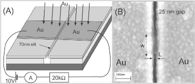
Nano-bridge fabrication process was discussed in detail in our prior publications. Anaya et al. (2003); Bowman et al. (2004); Anaya et al. (2004) In summary, samples were created by deposition of Au atoms in high vacuum () over two bulk Au films separated by a nm slit, as sketched in Fig. 1-A. A finite bias voltage is applied between the films and the resulting current is measured in situ. The deposition of Au is stopped as soon as a finite current is detected. In this way, only one contact is created.
The shape and the resistance of the contacts depends on growth conditions, such as bias voltage and background pressure. For example, we demonstrated that the resistance of the contact at high bias voltage can be increased reversibly by several orders of magnitude by increasing the partial water vapor pressure around the contact. Korotkov et al. (2003) In general, the growth process is quite complicated, because processes such as electromigration, surface atom diffusion, and intermixing with water molecules affect the contact shape and the disorder. Bowman et al. (2004)
The contacts selected in this work are grown at 10V using a limiting resistor of . The purpose of the limiting resistor is to reduce the current as soon as the contact is created, which prevents catastrophic electromigration processes.
One typical sample is shown in Fig. 1-B. The resistance of the contact is approximately inversely proportional to contact apparent width . Bowman et al. (2004) Thus, the resistance of the contact material is approximately uniformly distributed. The disorder length scale (grain size) is much smaller than the contact size .
In wide contacts (), and samples do not display Coulomb Blockade at our lowest temperature (). In narrow contacts (), and samples exhibit Coulomb Blockade at low temperatures. Bowman et al. (2004) Thus, in samples where , the electron localization length is comparable to .
I.2 Spin-Based Magnetofingerprints
We present quantum interference effects with magnetic field in devices with resistance , because these devices do not exhibit Coulomb Blockade at low temperatures, which makes it possible to study conductance fluctuations at the Fermi level, analogous to conductance fluctuations in weakly disordered metals. Webb et al. (1988) We select two new devices with resistances slightly below .
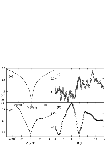
The I-V curves display a conductance suppression at zero bias voltage and at low temperatures (zero-bias anomaly or ZBA). This suppression is a Coulomb Blockade precursor. Anaya et al. (2004) Figs. 2-A and B display differential conductance versus in samples 1 and 2, respectively. is measured by lock-in technique with an excitation voltage . The ZBA was explained in detail by the theory of broadened Coulomb Blockade in a single electron transistor. Golubev et al. (1997)
Figs. 2-C and D display differential conductance versus magnetic field of samples 1 and 2 at zero DC-bias at base temperature. The conductance exhibits reproducible fluctuations with field. The fluctuation amplitude close to the universal value (). The fluctuations are sensitive to thermal cycling to room temperature, which demonstrates sensitivity of the fluctuations to impurity configurations. Thus, the fluctuations are analogous to the well known magnetofingerprints in mesoscopic physics.
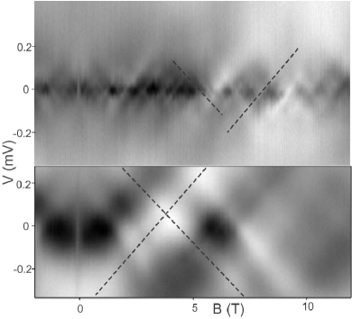
The magnetofingerprints in our samples are caused by the Zeeman effect. This is demonstrated in Fig. 3, which represents versus magnetic field and bias voltage. The figure displays a linear structure, which is highlighted by dashed lines of mathematical form . We investigated a set of 10 samples with resistances in range at milli-Kelvin temperature. The linear structure was found in every one of these samples. Since the slopes of the lines correspond to the Zeeman splitting, this confirms that the fluctuations with magnetic field are spin-based. By contrast, conductance fluctuations in weakly disordered metals are based on the Aharonov-Bohm effect and versus and versus are parametrically inequivalent.
In the next 2 sections of this paper, we will demonstrate that magnetofingerprints become spin based when the Drude mean free path becomes shorter than the Fermi wavelength. If the conducting material were homogeneous, this condition would not be physical because the Drude mean free path and the electron scattering length would be the same. But, if the system is not homogeneous, the Drude mean free path and the electron scattering length will not be the same and can be , even if the conducting material is a metal at .
II Granular Nano-bridge Model
In this section we introduce a model of electron transport through the nano-bridge. The model assumes that the disorder is granular with the grain size much smaller than . The grain diameter () is certainly smaller than our imaging resolution of roughly .
As discussed in the introduction, amorphous disorder is ruled out because Au does not alloy with the impurities that are responsible for disorder (). Granular disorder has been recently confirmed in samples created by electro-chemistry. Nieto et al. (2003); Grose et al. (2005) It has been shown that large electric fields near Au surfaces induce formation of Au nanoparticles of diameter of few nanometers, which assemble into a granular structure. Grose et al. (2005)
Theoretically, granular metals are similar to Fermi-Liquids. They are also known as Granular Fermi Liquids. Beloborodov et al. (2004) It has long been recognized that the Drude mean free path of a granular metal can be much shorter than the electron Fermi wavelength, Abeles et al. (1975); Imry (1997) because and the electron scattering length are not the same.
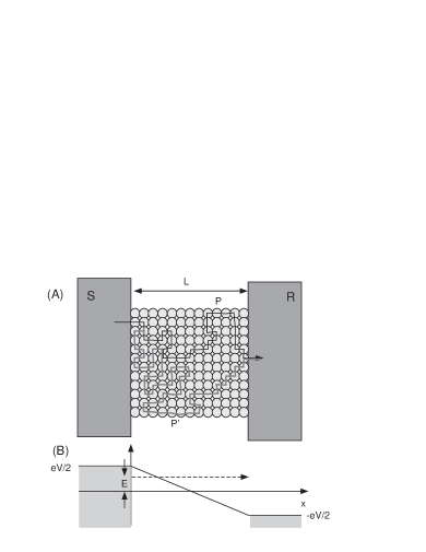
Consider a granular bridge of length in Fig. 4-A. The resistance of the bridge can be obtained using a 3D-resistor network model, because, by definition, the resistance between the grains () is larger than the resistance inside the grains (otherwise, the system would be homogeneous). The resistance of the network is , where is the sample cross-section area. The resistivity is obtained from , so .
In homogeneous systems, one can apply the Drude formula for resistivity , where is the electron scattering length. In granular systems, however, the Drude formula is not valid. But, one can still apply the Drude formula , where will be referred to as the nominal Drude mean free path. In a resistor network,
| (1) |
is not the same as electron scattering length ( for ballistic grains). One can change without changing , by changing .
We expect that the metal insulator transition occurs roughly when , where is the coordination number ( in our model). This condition is reasonable, because if the total resistance between a grain and its neighbors exceeds , then electron transport will be blocked by Coulomb-blockade and the system will be an insulator. Theoretical value for at the metal-insulator transition is similar to our estimate. Beloborodov et al. (2003)
A granular metal will satisfy the condition if the inter-grain resistance is in interval . At the metal-insulator transition, has a critical value , which can be several orders of magnitude shorter than .
In this paper, we investigate mesoscopic electron transport in this regime (). We will show that plays a crucial role in determining the origin of mesoscopic fluctuations with magnetic field.
Next, we discuss electron diffusion through granular systems. We assume that the average electron dwell time on any given grain is . After time , there are roughly hops between neighboring grains. If we assume that the hops are uncorrelated, then electron motion is diffusive, and the diffusion length is . Thus, the diffusion coefficient is .
In a homogeneous metal, the diffusion coefficient is . In a granular metal, this relationship is not valid. One can still apply this formula, , but will not be the same as and it will be referred to as the nominal diffusion mean free path. It follows that
Next, we investigate the relationship between the nominal Drude mean free path and the nominal diffusion mean free path. Let us assume that . Then , and after some algebra it can be shown that this is equivalent to
| (2) |
where is the level spacing inside the grains and is the resistance quantum.
This is the well known formula for the dwell time of an electron on a quantum dot connected to leads via resistance . Eq. 2 is undoubtedly correct, so it follows that . Thus, when examining electron transport over distances much larger than grain diameter, one can use a diffusion model with obtained from the resistor-network model(Eq. 1). Formula 2 is essentially the Einstein relation between diffusion and conductivity of a granular metal.
III Magnetofingerprints when
In this section, we explain the spin-based origin of conductance fluctuations () and discuss linear correlations in differential conductance with magnetic field and bias voltage . First we examine fluctuations in differential conductance at . Finite temperature effects are discussed in the appendix.
We will neglect the effects of spin-orbit scattering. In our prior publication, we demonstrated that spin-orbit scattering is suppressed because of the quantization of energy levels inside the grains. Anaya et al. (2004)
III.1 Magnetofingerprints as the Ericson’s fluctuations.
First we investigate conductance fluctuations with field at zero DC bias voltage. We find the conductance contribution from electrons with spin-up, . The differential conductance is given by the Landauer-Buttiker formula, Datta (2002)
| (3) |
where is the transmission probability of electrons with energy in magnetic field . By our convention, the energy in this equation is measured relative to the Fermi energy , i. e. for electrons with energy .
The magnetic field dependence in originates from the Aharonov-Bohm effect on the phase of the electron wavefunctions. We will neglect the Aharonov-Bohm effect, so that the dependence on the second argument can be omitted, i.e. . This approximation is valid if the applied magnetic flux through the sample is much smaller than the flux quantum. Later in the text, we discuss the validity of this assumption.
At zero bias voltage, is just the kinetic energy. The dependence of the transmission probability on arises because electron wavelength decreases with kinetic energy. This causes mesoscopic fluctuations known as the Ericson’s fluctuations. Ericson (1960) The Ericson’s fluctuations in mesoscopic conductors have not yet been measured directly.
Without Zeeman splitting, in Eq. 3 would be equal to . However, with Zeeman splitting included, the kinetic energy of spin-up electrons at the Fermi level increases with magnetic field. In particular, at the Fermi level the sum of the kinetic energy and the Zeeman energy equals . So , where is the g-factor, and is the Bohr magnetron. Consequently, Eq. 3 becomes
| (4) |
Taking into account electrons with spin down, the linear (zero-bias) conductance becomes
| (5) |
This equation demonstrates that magnetofingerprints are equivalent to the Ericson’s fluctuations. This behavior is possible only because we neglected the Aharonov-Bohm effect. The correlation energy is related to the correlation field : . At and , is given by the Thouless energy . Washburn and Webb (1992)
III.2 Conductance Fluctuations with Bias Voltage and the Ericson’s fluctuations
Now we consider the case when bias voltage is applied between the reservoirs. We choose a symmetric bias, in which the electrostatic potential of reservoir S is and the electrostatic potential of reservoir L is . We assume that reservoir is a source (). One would naively expect that the fluctuations of with are similar to the Ericson’s fluctuations, because increasing increases the kinetic energy of electrons that participate in transport.
We will assume that the energy is conserved in electron transport, i. e. the electron transport is horizontal, as sketched in Fig. 4-B. At , the quasi-Fermi level inside the sample varies with position. As a result, the kinetic energy varies with , so strictly speaking fluctuations will not be equivalent to the Ericson’s fluctuations.
The transmission probability depends on both electron energy and bias voltage. In further discussion, is the probability of transmission from S to R for electrons with energy at bias . is measured relative to the average Fermi level of the two reservoirs, as shown in Fig. 4-B.
In absence of inelastic electron scattering, the current through the sample is given by the Landauer-Buttiker formula, Datta (2002):
| (6) |
where is the Fermi function at and summation over indicates sum over electron spin polarization.
In the Landauer formalism, electron transport is horizontal, so the kinetic energy increases with position (), because the quasi-Fermi level decreases with x. The quasi-fermi level is defined as usual, as the position of the Fermi level that the electrons would assume if they were in local equilibrium (this would be the case if electron-phonon relaxation rate were much larger than the electron transport rate).
In good metals, the quasi-fermi level is very close to the electrostatic potential energy , where is the electrostatic potential and is the electron charge (). We assume that the electric field inside the sample is uniform, so for .
The transmission coefficient can be expressed as
| (7) |
where the sum is taken over incoming channels () in the left reservoir and all the outgoing channels () in the right reservoir, and is the transmission probability from channel into channel . can be expressed in terms of the probability amplitude for transfer from channel m to channel n, . Finally, the probability amplitude is equal to the sum over probability amplitudes of various Feynman paths connecting the reservoirs, Datta (2002)
| (8) |
where indicates an electron path and is the phase accumulated by an electron injected from reservoir S at energy along this path.
In the semiclassical approximation, , where is the kinetic energy of an electron on path at moment , and . So, and
This expression can be rewritten as
| (9) |
where .
The dependencies of on and are not equivalent, because phase contributions and are not directly proportional, since fluctuates among different paths. If is chosen so that an electron spends roughly the same time at different locations , as sketched in Fig. 4-A, then . If an electron spends significantly more time closer to one reservoir than to the other reservoir, which is sketched by path in Fig. 4-A, then .
We determined the statistical distribution of among different paths. To this end, we generated random-walks on 3D grids connecting two reservoirs. We find that the distribution of is a Gaussian with a probability density , where . The value of is important, because it will set the voltage range where V-fluctuations and the Ericson’s fluctuations are equivalent.
Next we obtain the differential conductance ,
| (10) |
Substituting the Fermi function at , we find
| (11) |
The Ericson’s fluctuations are represented by the dependencies on the first argument. If both and are varied simultaneously so that , then two out of the four terms in the sum on the right hand side of Eq. 11 will not fluctuate, which will lead to a linear structure in similar to our experimental observations.
The characteristic scales for the dependence of on the first argument are
| (12) |
The linear structure in will be significant if we can neglect the dependence on the second argument () and if we can neglect the dependence of the integral on the right hand side of Eq. 11 on and . Now we show that these two dependencies can indeed be neglected, which explains the linear structure in our experiments. In particular, we show that the correlation voltage for these two dependencies is much larger than .
The correlation energy () is roughly given by condition (Eq. 9) for a typical path P. Similarly, the characteristic voltage () for the second argument in is obtained from condition (Eq. 9). It follows that . The dependence on the second argument has three times larger correlation voltage than that in the first argument, explaining the pronounced linear structure in our experiments.
In conclusion, the conductance fluctuations with bias voltage are equivalent to the Ericson’s fluctuations and . The equivalence persists only in voltage range .
The integral in Eq. 11 also leads to fluctuations in conductance with and . It has been predicted by Larkin and and Khmelnitskii Larkin and Khmel’nitskii (1986) that this integral causes an increase in amplitude of conductance fluctuations at bias voltages larger than , by a factor of . The increase has been observed in Ag wires. Terrier et al. (2002)
Now we discuss the characteristic and of the integral. The integration over broadens the dependence of on magnetic field, thereby increasing the correlation field from to . Thus, the correlation voltage of the integral is set by the V-dependence in , and this correlation voltage is , six times larger than . So, the integral will not obscure the linear structure.
The dependencies of on the second argument and the integral are responsible for the asymmetry of conductance fluctuations around zero bias voltage.
To investigate different terms in Eq. 11, we make numerical simulations. We model our sample with a grid containing grains, and generate 2000 random walks across the sample. We calculate the phases along these random walks and obtain from the transmission amplitudes in Eq. 9. We assume that there is only one conducting channel, for simplicity, and sum the transmission amplitude over 2000 randomly selected paths . is plotted in Fig. 5-A. The pattern is streched along direction, which shows that that correlation scale for () is much smaller than correlation scale for (), in agreement with the analysis above.
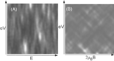
The differential conductance versus zeeman energy and bias voltage are plotted in Fig. 5-B. The linear structure is clearly significant and similar to our experimental observations. Note that there is a finite voltage range over which the lines in parameter space are resolved. This voltage range is roughly .
III.3 Absence of the Aharonov-Bohm Effect
We show that if , then quantum interference between paths and in Fig. 4-A will be more sensitive to the Zeeman effect than to the Aharonov-Bohm effect, which explains the spin-origin of magnetofingerprints in our samples. The characteristic magnetic field for the Aharonov-Bohm effect is given by the field for a flux quantum over sample area, . Washburn and Webb (1992) Using Eq. 12, we find , so if .
IV Dephasing Effects
In this section we discuss electron dephasing in our nano-bridges. Samples can be divided into two groups. In the first group, the conductance fluctuation amplitude and correlation scales and have strong and dependence. For example, in sample 1 conductance fluctuation amplitude decreases rapidly with . Fig. 6 displays root-mean-square differential conductance versus bias voltage at in sample 1. The linear structure is pronounced only near , which indicates the the correlation field increases with . Eight out of ten samples belong to the first sample group.

In the second group of samples, and at are independent of below an experimentally accessible temperature. In addition, base temperature values of and are independent of below a certain . This indicates that thermal broadening and dephasing are weak at low and , so correlation scales are set by the Thouless energy, . Sample 2 belongs to this group. Two out of ten samples belong to the second sample group. As discussed before, all ten samples have similar resistance. The origin of different sample groups will be discussed later in the section.
In the remainder of this section, we focus on the first group of samples. The dephasing time () can be obtained from the voltage dependence of the correlation field at base temperature. This method for measuring is different from that in standard mesoscopic physics of weakly disordered metals, where can be measured from the temperature dependence of . Mohanty and Webb (2002)
In our nano-bridges, magnetofingerprints are spin-based and is equal to the correlation energy. In Appendix 1 we find that if thermal broadening and dephasing are significant, then
| (13) |
where . (The factor of 2.9 is valid in a narrow temperature range ). is the dephasing time of electrons at energy above the Fermi level at temperature .
It is not possible to obtain the temperature dependence of the dephasing time from the temperature dependence , because is affected by both thermal broadening and dephasing. But, if is fixed, the energy dependence of the dephasing time can be obtained from Eq. 13.
To increase the statistics, we thermally cycled sample 1 between room temperature and base temperature 8 times. Fig. 7 shows the linear structure in 4 successive cool-downs, indicating that the data obtained in different thermal cycles are statistically uncorrelated. Even though thermal cycling scrambles the linear structure, the average conductance does not change with thermal cycling.
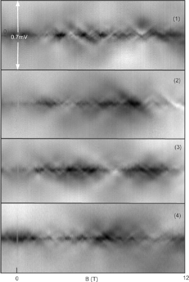
is calculated as the field at which the field autocorrelation function () decreases by 50, i.e. . The field autocorrelation function at temperature is found as
where over-line indicates averaging over magnetic field interval . Fig. 8-A displays the field autocorrelation function at at base temperature.
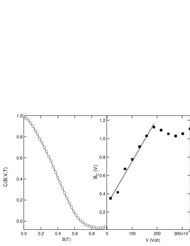
Next, we average the correlation field among different thermal cycles. The resulting correlation field versus bias voltage at base temperature is displayed in Fig. 8-B. Clearly, increases with . In voltage interval , the voltage dependence is approximately linear, and the best linear fit is
where the left hand side is in Tesla and is in volt.
As discussed above, the voltage dependence of the correlation field displays the energy dependence of the dephasing time. Substituting for the average electron energy injected from the Fermi level of the source, we find
| (14) |
At energy , the offset in this equation can be neglected. Similarly, at large energy (), the offset in Eq. 13 can be neglected, so comparing Eq. 13 and Eq. 14, we find
| (15) |
It follows that the correlation energy of an electron with energy above the Fermi level is equal to . Before we discuss the physical meaning of this observation, we examine the correlation scale at zero bias voltage.
At , the correlation energy is . This value is reasonable if we assume that the base electron temperature is . In particular, at , the average electronic energy is given by the full-width-half-maximum of the derivative of the Fermi function (). So, . Substituting , we obtain . is a reasonable value for our base electron temperature, because the wires were filtered at the base phonon temperature ().
We believe that the equation demonstrates a break-down of the Fermi-Liquid description of electron transport in our samples. The selected samples have conductance comparable to the conductance quantum. Coulomb Blockade in these samples is barely suppressed and the localization length is comparable to sample size. We expect that the Fermi-liquid picture in this regime begins to fail, which causes the energy uncertainty of a quasiparticle with energy to be comparable to . So, the correlation energy is comparable to the excitation energy.
Now we discuss the variation of the Thouless energy among devices with a similar resistance. The Thouless energy is directly related to the electron diffusion time across the device, which implies that the electron diffusion time varies among different samples. The diffusion time is shorter than the thermal time () in two out of ten samples with resistance slightly below the resistance quantum.
The conductance-fluctuation amplitude is comparable to in all ten samples. This implies that in the eight samples where the Thouless energy is , the Thouless energy cannot be . If we assume the opposite, then the conductance-fluctuation amplitude will be suppressed by , Lee et al. (1987) contrary to the data. So, the diffusion time in our samples varies roughly within an order of magnitude.
The fluctuations in the diffusion time among samples with similar resistance can be explained by the fluctuations in sample dimensions and . The fabrication process is based on electromigration and we do not have precise control over these dimensions. We found through scanning electron microscopy that the conductance is only roughly proportional to the apparent width w. The conductance per unit width varies within a factor of 3 among different samples. Since the diffusion time scales as and the selected ten samples have similar resistance, the diffusion time can vary by factor of , even if we assume that the resistivity does not vary among samples. This can explain the observed variation in the Thouless energy among samples.
The fact that the fluctuation in the diffusion time among samples is within an order of magnitude indicates that our sample parameter control is also within an order of magnitude. We think that this sample control is quite good, in the light that the nanojunctions were self-created through electromigration.
V Appendix: Derivation of the Correlation Field at finite temperature
At finite temperature, Eq. 10 still applies, but with replaced with the Fermi function at temperature . The formula takes into account thermal broadening effects, but it neglects dephasing.
First we account for the thermal broadening. In Eq. 11, which is valid at , we found that the correlation voltage of the integral is three times larger than that for the first term on the right hand side of the equation. Thus, to find the temperature dependence in the limit of small , we only need to find the correlation voltage of the first integral in Eq. 10. The effect of the second integral in Eq. 10 on is weak if .
If we neglect the integrals in Eqs. 11 and 10, the conductance becomes
at and
at . It follows that
| (16) |
In this approximation, the conductance fluctuations at can be obtained by convolving the conductance fluctuations at with the derivative of the Fermi function. We reiterate that we neglected the conductance contributions with larger correlation scales.
It follows that the field correlation function at temperature is proportional to
where is the field correlation function at . We can make an approximation , because the thermal of () is much larger the width of (the Thouless energy). So, the field correlation function at temperature becomes proportional to the autocorrelation function of the derivative of the Fermi function. The correlation field is the half-width-half-maximum of the autocorrelation function of (which is ), so
In the presence of dephasing, the correlation energy is increased by energy uncertainty . Datta (2002). So, the correlation field becomes
In good Fermi liquids, one can neglect the dephasing term.
VI conclusion
We show experimentally and theoretically that quantum interference effects with magnetic field in highly disordered Au nanobridges are governed by the Zeeman effect. The Aharonov-Bohm effect is suppressed when the nominal Drude mean free path is smaller than the Fermi wavelength. Using the Landauer-Buttiker formalism, we show that both magnetofingerprints and conductance fluctuations with bias voltage are equivalent to the Ericson’s fluctuations. This permits measurements of the correlation energy from the correlation field. If sample size is comparable to the localization length, then the correlation energy of electrons at energy will be , which shows that the Fermi liquid description breaks down at the localization length-scale.
This work was performed in part at the Cornell Nanofabrication Facility, (a member of the National Nanofabrication Users Network), which is supported by the NSF, under grant ECS-9731293, Cornell University and Industrial affiliates, and the Georgia-Tech electron microscopy facility. This research is supported by the David and Lucile Packard Foundation grant 2000-13874 and the NSF grant DMR-0102960.
References
- Morpurgo et al. (1999) A. F. Morpurgo, C. M. Marcus, and D. B. Robinson, Appl. Phys. Lett. 74, 2084 (1999).
- Park et al. (1999) H. Park, A. K. L. Lim, A. P. Alivisatos, J. Park, and P. L. McEuen, Appl. Phys. Lett. 75, 301 (1999).
- Li et al. (1999) C. Z. Li, A. Bogozi, W. Huang, and N. J. Tao, Nanotechnology 10, 221 (1999).
- Yu and Natelson (2003a) L. H. Yu and D. Natelson, Appl. Phys. Lett. 82, 2332 (2003a).
- Yu and Natelson (2003b) L. H. Yu and D. Natelson, Phys. Rev. B 68, 113407 (2003b).
- Bowman et al. (2004) M. Bowman, A. Anaya, A. L. Korotkov, and D. Davidovic, Phys. Rev. B 69, 205405 (2004).
- Boussaad and Tao (2002) S. Boussaad and N. J. Tao, Appl. Phys. Lett. 80, 2398 (2002).
- Chan et al. (2005) I. H. Chan, R. M. Clarke, C. M. Marcus, K. Campman, and A. C. Gossard, Analytical Chemistry 77, 243 (2005).
- Anaya et al. (2004) A. Anaya, M. Bowman, and D. Davidović, Phys. Rev. Lett. 93, 246604 (2004).
- Anaya et al. (2003) A. Anaya, A. L. Korotkov, M. Bowman, J. Waddell, and D. Davidović, Journal of Applied Physics 93, 3501 (2003).
- Nieto et al. (2003) F. J. R. Nieto, G. Andreasen, M. E. Martins, F. Castez, R. C., and S. A. J. Arvia, J. Phys. Chem. B 107, 11452 (2003).
- Grose et al. (2005) J. E. Grose, A. N. Pasupathy, D. C. Ralph, B. Ulgut, and H. D. Abruna, Phys. Rev. B. 71, 035306 (2005).
- Washburn and Webb (1992) S. Washburn and R. A. Webb, Rep. Prog. Phys. 55, 1311 (1992).
- Imry (1997) Y. Imry, Introduction to mesoscopic physics (Oxford University Press, 1997).
- Abeles et al. (1975) B. Abeles, P. Sheng, M. D. Coutts, and Y. Arie, Adv. Phys. 23, 407 (1975).
- Korotkov et al. (2003) A. L. Korotkov, M. Bowman, H. J. McGuinness, and D. Davidovic, Nanotechnology 14, 42 (2003).
- Mott and Davis (1979) N. F. Mott and G. A. Davis, Electronic Properties of Nanocrystalline Materials (2d ed. Clarendon Press, 1979).
- Webb et al. (1988) R. A. Webb, S. Washburn, and C. P. Umbach, Phys. Rev. B 37, 8455 (1988).
- Golubev et al. (1997) D. S. Golubev, J. Konig, H. Schoeller, G. Schon, and A. D. Zaikin, Phys. Rev. B 56, 15782 (1997).
- Beloborodov et al. (2004) I. S. Beloborodov, A. V. Lopatin, and V. M. Vinokur, Phys. Rev. B 70, 205120 (2004).
- Beloborodov et al. (2003) I. S. Beloborodov, K. B. Efetov, A. V. Lopatin, and V. M. Vinokur, Phys. Rev. Lett. 91, 246801 (2003).
- Datta (2002) S. Datta, Electronic transport in mesoscopic systems (Cambridge University Press, 2002).
- Ericson (1960) T. Ericson, Phys. Rev. Lett. 5, 430 (1960).
- Larkin and Khmel’nitskii (1986) A. I. Larkin and D. E. Khmel’nitskii, Zh. Eksp. Teor. Fiz. 91, 1815 (1986), sov. Phys. JETP 64, 1075, 1075 (1986).
- Terrier et al. (2002) C. Terrier, D. Babic, C. Strunk, T. Nussbaumer, and C. Schonenberger, Europhys. Lett. 59, 437 (2002).
- Mohanty and Webb (2002) P. Mohanty and R. A. Webb, Phys. Rev. Lett. 88, 146601 (2002).
- Lee et al. (1987) P. A. Lee, A. D. Stone, and H. Fukuyama, Phys. Rev. B 35, 1039 (1987).