Charge and spin density modulations in semiconductor quantum wires
Abstract
We investigate static charge and spin density modulation patterns along a ferromagnet/semiconductor single junction quantum wire in the presence of spin-orbit coupling. Coherent scattering theory is used to calculate the charge and spin densities in the ballistic regime. The observed oscillatory behavior is explained in terms of the symmetry of the charge and spin distributions of eigenstates in the semiconductor quantum wire. Also, we discuss the condition that these charge and spin density oscillations can be observed experimentally.
pacs:
73.21.Hb, 71.70.Ej, 72.25.Hg, 03.65.NkI Introduction
Relativistic quantum mechanics has predicted a rapid oscillatory behavior of free electrons, called Zitterbewegung, which is due to the interference between the positive- and negative-energy components in the wave packet.Sakurai67 This peculiar oscillation happens because the velocity is not a constant of motion even in the absence of any potential and has a fluctuating component, while the momentum commutes with the Hamiltonian. Recently, from the analogy between the band structure of semiconductor quantum wells and relativistic electrons in vacuum, it has been pointed out that electrons in semiconductors undergo the same oscillatory motion.Schliemann04 ; Zitterbewegung The essential mechanism causing such a motion is the spin-orbit (SO) coupling in the semiconductor. In a two-dimensional electron gas confined in a heterostructure quantum well, two SO coupling effects are usually taken into account: the Rashba Rashba84 and Dresselhaus Dresselhaus55 SO coupling effects described by the following expressions
| (1) |
respectively, where are the Pauli matrices. The strength of each SO coupling is measured in terms of characteristic wave vectors and , respectively. The Rashba term arises when the confining potential of the quantum well lacks inversion symmetry, while the Dresselhaus term is due to bulk inversion asymmetry. In the presence of SO coupling, the velocity of the electron is not a constant of motion:
| (2) |
The spin precession due to the SO coupling eventually leads to a fluctuating velocity and consequently an oscillating motion of the electron.
While the oscillatory behavior of the electron is dynamic in the original proposal of the Zitterbewegung, it is highly plausible that one can observe static patterns of charge density oscillation in some properly-structured semiconductor samples.
In our paper we investigate static charge and spin density oscillations along a ferromagnet/semiconductor single junction quantum wire in the ballistic limit. The charge and spin densities across the system are calculated using coherent scattering theory. The observed oscillatory behaviors are explained in terms of the symmetric or antisymmetric structure of charge and spin distributions of eigenstates in the semiconductor quantum wire. Also, we discuss the condition that these charge and spin density oscillations can be observed experimentally.
Our paper is organized as follows: In Sec. II we investigate the properties of eigenstates of semiconductor quantum wires, paying attention to their symmetric structures in charge and spin density distributions. The effect of SO coupling on the structures in the presence of a confinement potential is examined in detail. Section III is devoted to the numerical calculation of charge and spin density modulations in the ferromagnet/semiconductor single junction system in the presence of SO coupling. The main results are summarized in Sec. IV.
II Property of Eigenstates in Semiconductor Quantum Wires
Previous works Mireles01 ; Governale02 have shown that perturbation theory cannot correctly explain the effect of moderate or large SO coupling on energy levels and properties of eigenstates in semiconductor quantum wires. Instead, truncating the Hilbert space to the lowest bands Governale02 ; Schliemann04 or tight-binding models Mireles01 were successfully used to investigate the role of SO coupling on the transport through quantum wires. Here, we have implemented an exact numerical method of solving the system with arbitrary strength of SO coupling. Before introducing the method and discussing the properties of the states obtained numerically, we briefly review the structure of the system Hamiltonian and its symmetry in terms of transverse modes.
II.1 Hamiltonian and Symmetry Properties
We consider a quasi-one-dimensional system of electrons in the presence of SO coupling:
| (3) |
where and are two-dimensional position and momentum vectors and is the effective mass of the electrons in the semiconductor. The electrons are confined in the direction by an infinite square-well potential of width ,
| (4) |
We assume that the SO Hamiltonian consists of and , see Eq. (1). In some semiconductor heterostructures (e.g., InAs quantum wells) dominatesDas90a , and in others (e.g., GaAs quantum wells) is comparable to Lommer88a . A series of experiments RashbaExp has demonstrated that the strength of the Rashba SO coupling can be tuned by external gate voltages. Note that our choice of the square-well confinement eliminates the possibility of SO coupling due to effective electric fields coming from the nonuniformness of the confining potential. This kind of SO coupling should be considered in case of parabolic confining potential.Moroz99
It is instructive to rewrite the Hamiltonian in Eq. (3) in second-quantized form to gain insight into the effect of SO coupling on the transverse modes. To this end, we define / to be the annihilation/creation operators of the th transverse mode with a wave vector and a spin branch index in the absence of SO couplings. It is convenient to choose the spin polarization axis to be along the effective magnetic field due to the SO coupling for waves propagating in the -direction such that
| (5) |
with .Lee04 In terms of these operators, the Hamiltonian is expressed as
| (6) |
This expression shows that SO coupling leads to two effects. On one hand, it lifts the spin degeneracy by shifting the energies of the transverse modes such that
| (7) |
with and . On the other hand, it mixes the transverse modes according to the amplitudes given by
| (8a) | ||||
| (8b) | ||||
As shown in Eq. (8), the SO coupling mixes transverse modes with opposite parities and possibly opposite spins. Therefore, the eigenstates of the Hamiltonian in Eq. (6) are generally not symmetric or antisymmetric.
Still, the charge and spin density pattern can be symmetric or antisymmetric: For simplicity, we focus on the case when only one of two SO coupling terms exists, that is, . In this case, for any symmetric confinement potential satisfying , the Hamiltonian commutes with the so-called “spin parity” operator , where is the inversion operator for the -component such that .Bulgakov99 The eigenstates of the system should thus also be eigenstates of the spin parity operator, having the eigenvalues , which is evident from the fact that . Denoting to be the wave function of an eigenstate for wave vector , subband index , and quantum number of spin parity , one can show that the spin density components for should be antisymmetric with respect to ,Governale02 ; Debald04 while the charge density and the spin component for are symmetric. For example, . This (anti)symmetric properties for persist even in case , when there is no simple operator like commuting with the Hamiltonian. However, as and are tuned to come close to each other, the antisymmetric components decrease in magnitude and even vanish when since the off-diagonal terms in the matrix that couple modes with opposite spins vanish. Interestingly, for , the spin operator itself commutes with the Hamiltonian and the SO coupling couples only the transverse modes with the same spin (see Eq. (8b)) so that a common spin quantization axis can be defined for all the eigenstates.Schliemann03
The symmetry properties discussed up to now are not restricted to the square-well potential case. One can show that the same reasoning works in the case of a harmonic potential.Debald04 All that one should do is to redefine the amplitude according to the confinement potential. For the symmetric potential satisfying , the amplitude has nonzero values only when and have opposite parities and reproduces the same symmetry properties as discussed above. Hence, the choice of confinement potential does not lead to any qualitatively different effect. Therefore, we focus on the square-well potential since it is convenient for numerical calculations.
II.2 Numerical Calculation of Eigenstates
It is possible to obtain the eigenstates numerically by diagonalizing the Hamiltonian Eq. (6) in a truncated basis of transverse modes. Since we need eigenstates at a given energy, not a given wave vector, we have adopted another numerical method to obtain the eigenstates: First, prepare eigenstates at a given energy in the absence of the confinement potentialLee04 and then numerically find a set of wave vectors such that the linear superposition of four eigenstates sharing the same wave vector satisfies free boundary conditions at the infinite walls, that is, vanishes at . This method is superior to the diagonalization of the Hamiltonian in two aspects; one can obtain numerically exact eigenstates in this way, and an infinite set of evanescent waves, that is, eigenstates with complex at the targeted energy can be found systematically. Evanescent waves turned out to be important in transport through (semi-)finite samples.Lee04
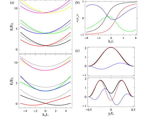
First, we consider the case where only Rashba SO coupling is present (). Figure 1 shows the spectra of this system and the properties of the eigenstates for weak and strong SO coupling. Small SO coupling () splits the spin degeneracy according to Eq. (7) (see the upper figure in Fig. 1(a)) and each spin branch keeps its spin polarization direction approximately such that as long as is not so large (). Due to the antisymmetry of the spin distribution, the spin expectation values and strictly vanish irrespective of the SO coupling strength. However, the spin density component is finite and has opposite sign for different branches: . As increases, on the other hand, the mixing of the transverse modes with opposite spins becomes more apparent such that level crossings happen even in the same subband for (see the lower figure in Fig. 1(a)) and the spin polarization is changed and even reversed compared to the case of weak SO coupling. Figure 1(b) shows that at strong SO coupling and large the spins of two branches in the lowest subband are polarized parallel to each other: for both .Governale02 This is due to mixing with higher-subband states having opposite spin, which manifests itself well in Fig. 1(c) where the charge density profile of the state of the lowest subband exposes the contribution from the higher subband . The charge and spin density profiles in Fig. 1(c) also confirm the (anti)symmetric structure proven based on the symmetry of the system.
Dresselhaus SO coupling , related to by a unitary transformation , gives rise to an energy spectrum and charge and spin density profiles identical to those obtained in the Rashba SO coupling case except for the rotation of spin axes such that , , and and the substitution of by .
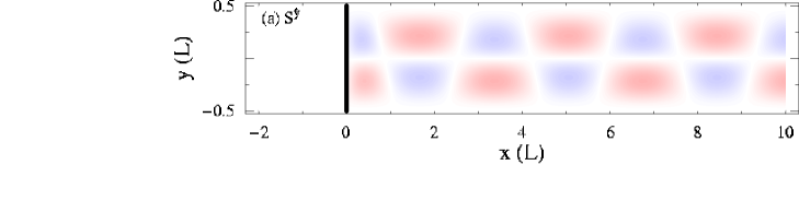
In the presence of both Rashba and Dresselhaus SO coupling terms, the spin polarization of the eigenstates is not along the - or -axes any longer, since there are nonzero spin expectation values and , and its direction depends on the ratio . Nevertheless, as shown in Fig. 2, the spin density profiles are found to have (anti)symmetric structures similar to the previous cases: and . Note that both spin- and components are symmetric. The antisymmetric component is observed to decrease in magnitude as approaches , and eventually vanishing when . This behavior, consistent with the argument in terms of coupling matrix elements of in Eq. (8b), indicates that whereas Rashba and Dresselhaus SO coupling can induce an antisymmetric distribution of separately, the presence of both of them will lead to a reduction in .
In summary, SO interaction in the presence of a symmetric confining potential can result in antisymmetric structures in the spin distributions of individual eigenstates, especially in the spin- component. This phenomenon manifests itself strongly when either Rashba or Dresselhaus SO coupling is present and vanishes as both coupling strengths become equal to each other.
III Charge and Spin Modulations in the Presence of Spin-orbit Coupling
In this section we investigate the charge and spin density modulations in a ferromagnet/semiconductor single junction quantum wire. Static charge and spin density oscillations are induced by injecting a spin-polarized current from ferromagnet to semiconductor. We make use of the coherent scattering theory to calculate the charge and spin density modulations in the ballistic regime and uncover the fact that the (anti)symmetric structure of eigenstates in semiconductor quantum wires studied in the previous section is deeply related to such density oscillations.
III.1 Scattering Theory
The single junction system consists of the ferromagnet (F; ) and the semiconductor (S; ) regions confined by the square-well potential of width . While the electrons in the semiconductor region are governed by Eq. (3), the Hamiltonian for the ferromagnet region is
| (9) |
The spin-splitting energy is assumed to be very large compared to other energy scales such that only the majority spin state (spin up state) is available at the energy of interest. Here we have assumed that both regions have identical effective masses and lower band edges, because the impedance mismatch due to a difference in them does not affect the density oscillation in a qualitative way. In order to set up the scattering theory one should construct a set of eigenstates in both regions at a given energy . Denote to be eigenstates in the ferromagnet/semiconductor regions propagating in the or direction at energy , where is a composite index with subband index and spin index and is a spinor for the state. Note that the wave vector can be complex-valued in the case of evanescent waves.
The boundary conditions at the interface are then specified by the following two equations:
| (10a) | ||||
| (10b) | ||||
for all . Here the wave functions in both regions can be expanded in terms of the eigenstates as follows: and with complex coefficients . The velocity operators, and differ from each other due to the presence of SO coupling in the semiconductor.
The SO coupling deforms the transverse modes such that they do not match in the ferromagnet and semiconductor regions. It is thus impossible to reduce the scattering problem to a one-dimensional one. Instead we set up an infinite number of coupled linear equations for the coefficients by multiplying on both sides of Eqs. (10a) and (10b) and integrating them over . The coupled linear equations are then solved numerically for the reflection/transmission coefficients at given incident coefficients . In our study we focus on the injection of the electron through the lowest transverse mode such that and the other incident coefficients are zero. Since the contribution of evanescent waves in high subbands is very small in this case, the coupled equations can be truncated to be of finite dimensions with negligible errors. By using the coefficients obtained in this way, we calculate and investigate the charge and spin density profiles, and in the next sections.
III.2 Charge Oscillation due to Spin-orbit Coupling
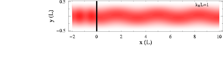
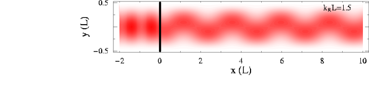
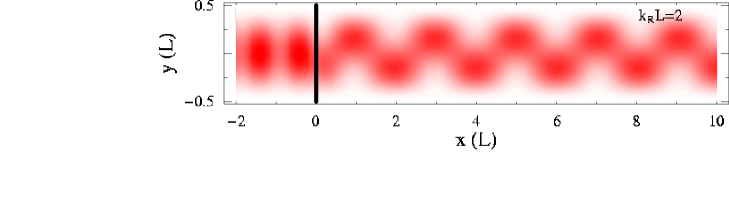
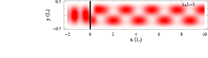
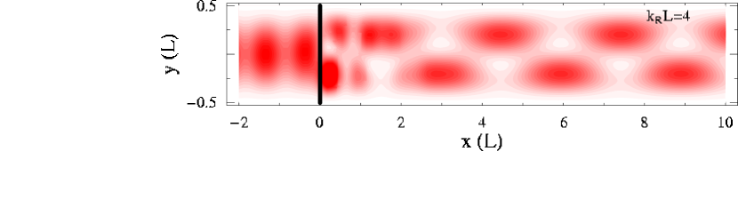
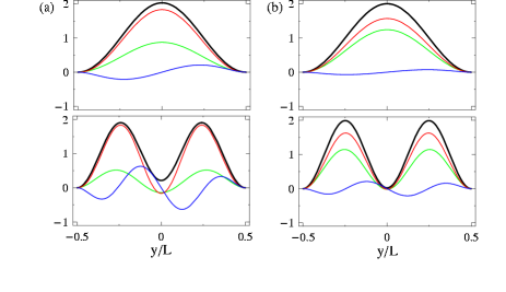
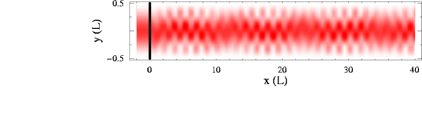
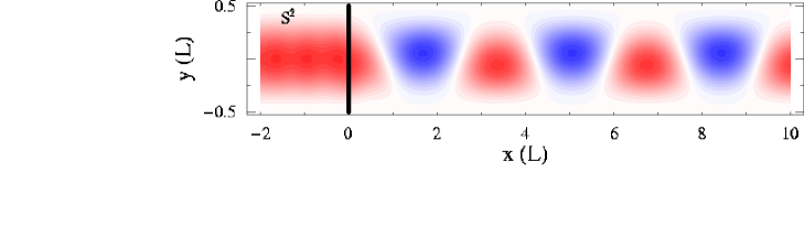
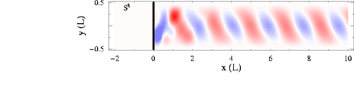
First, we investigate the charge density oscillation due to Rashba SO coupling and focus on the energy levels for which only two propagating states exist in the semiconductor region. Figure 3 shows the charge density profiles near the ferromagnet/semiconductor junction for various strengths of the Rashba SO coupling and clearly disclose the static oscillatory patterns perpendicular to the propagating direction. The patterns oscillate around the center line of the wire and the oscillation amplitude increases with the coupling strength . For large SO coupling the electron does not stay any longer near the center line, forming high-density islands off-center. This oscillation is related to the fact that two propagating waves are eigenstates of the spin parity operator with opposite eigenvalues . From this property one can prove that the charge density can be divided into symmetric and antisymmetric parts with respect to :
| (11) |
While the symmetric component is uniform along the wire, the antisymmetric part oscillates along the -direction with period and generates the density modulations shown in Fig. 3. Here, is the wave vector difference of two propagating modes.
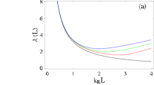
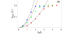
The oscillation period depends on both the SO coupling strength and the energy of the incident electron, as shown in Fig. 4(a). At weak SO couplings the period is determined by the characteristic wave vector such that it decreases like regardless of the energy. As increases further, on the other hand, the period increases with , having a minimum. In addition, the period gets longer at higher energies. The non-monotonic behavior of the period is another manifestation of mixing between transverse modes due to the SO coupling. Figure 4(b) shows the dependence of the oscillation amplitude on the SO coupling strength and the energy. Here the oscillation amplitude is given by the distance between the center line and the points where the density reaches its maximum. The parabolic dependence of on at small SO couplings indicates that the charge density oscillation is a second-order effect of the SO coupling. As is increased, the amplitude does not increase any longer and instead saturates to as long as the condition on the number of propagating waves is not violated.
At higher energies more than two propagating waves are involved in the scattering process in the semiconductor region and the charge density oscillation pattern due to their interference cannot be specified by one period. Instead, some beating patterns appear as shown in Fig. 5. While the SO coupling still leads to oscillatory motion of the charge, oscillations of short and long periods are mixed and the pattern becomes complicated.
Our observation is related to the prediction of Schliemann and LossSchliemann04 about the oscillatory behavior of free electrons in the presence of Rashba SO coupling: the center of an electron wave packet oscillates in the direction perpendicular to its group velocity with the frequency , giving rise to the oscillation period along the propagating direction. Controlled steady injection of wave packets with the same can produce the static density modulations we have observed. They also studied the dynamic oscillation of an electron with a given momentum in quantum wires, where the electron is prepared initially in the lowest-lying spin-polarized states. In this case, since the initial state is not an energy eigenstate, dynamic beating patterns due to the interference of waves with different energies are observed. On the other hand, our static density oscillation patterns are due to the interference of the energy eigenstates with a given energy. For that reason, such beating patterns and the resonance phenomena, leading to the sharp peak in the oscillation amplitude, are absent in our observation.
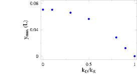
We now include the effect of the Dresselhaus SO coupling on the charge density modulation. The unitary relation between two SO terms and discussed in Sec. II guarantees that the Dresselhaus SO coupling results in exactly the same charge density oscillation as the Rashba SO coupling. In the presence of both coupling terms, however, the oscillation vanishes as the strengths of two terms become equal to each other. Figure 6 shows that the amplitude of the oscillation decreases with for finite and the oscillation disappears when . This tendency is quite similar to the dependence of the antisymmetric distribution of on the SO coupling. It also supports the close relation between the charge density oscillation and the antisymmetric structure of eigenstates in semiconductor quantum wires.
Before closing this section we address the experimental observability of the charge density modulations. Since the oscillation patterns depend on the energy of the incident electron, it should be checked whether the superposition of charge density patterns from different energies can weaken the overall density oscillation. Figure 4(a) shows that for large SO coupling the period strongly depends on the energy. Therefore, in the case of a large voltage drop across the junction the injection of electrons with a wide range of energy will smear the density modulation by superposing density patterns oscillating with different periods. For small SO coupling, on the other hand, the phase as well as the oscillation period pattern are weakly dependent on the energy, leading to the superposition of commensurate density patterns. In addition, the states below the fermi level are irrelevant to the charge density oscillation because the levels are filled incoherently such that their charge distributions are always symmetric with respect to . Hence the condition for the observation of charge density oscillation is that either the SO coupling strength or the applied voltage across the junction should be small enough. Under this condition, charge oscillations can be detected via high-resolution scanning probe microscopy techniquesSTM by imaging the charge density directly or by measuring the change of conductance along the quantum wire as a function of the position of a tip that can deplete charges under it.Schliemann04
III.3 Spin Oscillation due to Spin-orbit Coupling
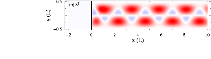
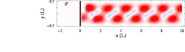
In the presence of SO coupling the electron spin precesses in the effective magnetic field that depends on the momentum. Spin density patterns thus reflect such spin precession as well as the charge density distribution discussed in the previous section. Figure 7 shows spin density profiles along the quantum wire if only Rashba SO coupling is present. The spin precessing patterns in indicate that the effective magnetic field is approximately perpendicular to the electron’s moving direction. The spin distribution is not symmetric with respect to in the semiconductor region and this behavior gets stronger as the SO coupling increases. It is because the spin pattern follows the charge density oscillation that is also asymmetric. While for all , is nonvanishing inside the semiconductor, increasing in magnitude with the SO coupling strength. Unlike , get biased to positive values as is increased, indicating a spin polarization along the -direction. This is a direct consequence of the spin polarization of the lowest modes at large and (see Sec. II.2).
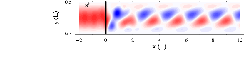
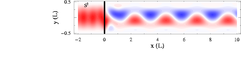
The Dresselhaus SO coupling also gives rise to similar spin profiles; the spin axes and are exchanged, and the spin distributions are mirror-reflected with respect to . In the presence of both coupling effects, on the other hand, the spin density patterns, with all the components nonvanishing, become distorted as shown in Fig. 8. Slanted patterns appear due to the absence of any symmetry with respect to . As long as , the spin is preferentially polarized along either - (when ) or - (when ) direction. For an unbiased spin precession takes place for all the spin components.
Under the same condition found for the detection of charge density modulations, the spin density distributions can be experimentally observed. Spin-polarized scanning tunneling microscopyYamada03 with magnet-coated tips or optical techniques such as the spatially resolved Faraday rotation spectroscopyKato04 can produce high-resolution images of spin density profiles.
IV Conclusion
We have investigated the symmetry properties of eigenstates in semiconductor quantum wires and observed the charge and spin density modulations along quantum wires consisting of a ferromagnet/semiconductor junction by using the coherent scattering theory. We have shown that the Rashba or Dresselhaus SO coupling terms induce charge density oscillations perpendicular to the propagating direction and that the (anti)symmetric structure of charge and spin distributions in eigenstates is deeply related to the oscillations. Charge and spin density oscillations can be experimentally observed as long as the SO coupling strength or the voltage drop across the junction are small enough.
Impurities, dirty interfaces, and electron-electron interactions that are not included in our study affect the transport in low-dimensional systems. Although these effects will therefore influence the form of the charge density modulations and make it more homogeneous, the charge density modulation may still be observed in sufficiently clean and low-density samples.
Acknowledgements.
We would like to thank W. Belzig, M.-S. Choi, and J. Schliemann for helpful discussions. This work was financially supported by the SKORE-A program, the Swiss NSF, and the NCCR Nanoscience.References
- (1) J.J. Sakurai, Advanced Quantum Mechanics (Addison Wesley, Reading, 1967).
- (2) J. Schliemann, D. Loss, and R.M. Westervelt, cond-mat/0410321.
- (3) Z.F. Jiang, R.D. Li, Shou-Cheng Zhang, and W.M. Liu, cond-mat/0410420; W. Zawadzki, cond-mat/0411488.
- (4) Y.A. Bychkov and E.I. Rashba, J. Phys. C 17, 6039 (1984).
- (5) G. Dresselhaus, Phys. Rev. B 100, 580 (1955).
- (6) F. Mireles and G. Kirczenow, Phys. Rev. B 64, 24426 (2001).
- (7) M. Governale and U. Zülicke, Phys. Rev. B 66, 73311 (2002).
- (8) B. Das, S. Datta, and R. Reifenberger, Phys. Rev. B 41, 8278 (1990); G.L. Chen, J. Han, T.T. Huang, S. Datta, and D.B. Janes, Phys. Rev. B 47, R4084 (1993); J. Luo, H. Munekata, F.F. Fang, and P.J. Stiles, Phys. Rev. B 41, 7685 (1999).
- (9) G. Lommer, F. Malcher, and U. Rossler, Phys. Rev. Lett. 60, 728 (1988); B. Jusserand, D. Richards, H. Peric, and B. Etienne, Phys. Rev. Lett. 69, 848 (1992); B. Jusserand, D. Richards, G. Allan, C. Priester, and B. Etienne, Phys. Rev. B 51, R4707 (1995).
- (10) J. Nitta, T. Akazaki, H. Takayanagi, and T. Enoki, Phys. Rev. Lett. 78, 1335 (1997); G. Engels, J. Lange, Th. Schäpers, and H. Lüth, Phys. Rev. B 55, R1958 (1997); D. Grundler, Phys. Rev. Lett. 84, 6074 (2000); T. Koga, J. Nitta, T. Akazaki, and H. Takayanagi, Phys. Rev. Lett. 89, 46801 (2002).
- (11) A.V. Moroz and C.H.W. Barnes, Phys. Rev. B 60, 14272 (1999).
- (12) M. Lee and M.-S. Choi, cond-mat/0407337.
- (13) E.N. Bulgakov, K.N. Pichugin, A.F. Sadreev, P. Streda, and P. Seba, Phys. Rev. Lett. 83, 376 (1999).
- (14) S. Debald and B. Kramer, cond-mat/0411444.
- (15) J. Schliemann, J.C. Egues, and D. Loss, Phys. Rev. Lett. 90, 146801 (2003).
- (16) M.A. Topinka, B.J. LeRoy, S.E.J. Shaw, E.J. Heller, R.M. Westervelt, K.D. Maranowski, and A.C. Gossard, Science 289, 2323 (2000); B.J. LeRoy, J. Phys.: Condens. Matter 15, R1835 (2003).
- (17) T.K. Yamada, M.M.J. Bischoff, G.M.M. Heijnen, T. Mizoguchi, and H. van Kempen, Phys. Rev. Lett. 90, 056803 (2003).
- (18) Y. Kato, R.C. Myers, A.C. Gossard, and D.D. Awschalom, Nature 427, 50 (2004).