Heterovalent interlayers and interface states: an ab initio study of GaAs/Si/GaAs (110) and (100) heterostructures
Abstract
We have investigated ab initio the existence of localized states and resonances in abrupt GaAs/Si/GaAs (110)- and (100)-oriented heterostructures incorporating 1 or 2 monolayers (MLs) of Si, as well as in the fully developed Si/GaAs (110) heterojunction. In (100)-oriented structures, we find both valence- and conduction-band related near-band edge states localized at the Si/GaAs interface. In the (110) systems, instead, interface states occur deeper in the valence band; the highest valence-related resonances being about 1 eV below the GaAs valence-band maximum. Using their characteristic bonding properties and atomic character, we are able to follow the evolution of the localized states and resonances from the fully developed Si/GaAs binary junction to the ternary GaAs/Si/GaAs (110) systems incorporating 2 or 1 ML of Si. This approach also allows us to show the link between the interface states of the (110) and (100) systems. Finally, the conditions for the existence of localized states at the Si/GaAs (110) interface are discussed based on a Koster-Slater model developed for the interface-state problem.
pacs:
73.20.-r, 73.20.At, 73.40.TyI Introduction
In recent years, a large amount of theoretical and experimental work has been concentrated on heterostructures composed of ultrathin layers of a given group-IV material deposited at III-V/III-V or II-VI/II-VI homo- or hetero- junctions.alfonso Interest in these systems has been stimulated by the possibility of tuning the band discontinuity in heterojunctions, or inducing a band discontinuity in homojunctions, thus allowing more flexibility in designing novel devices.capasso In particular, model calculations,walter supported by ab initio computations,mariapert have indicated that Si inserted as a bilayer at a GaAs/AlAs (100) heterojunction or at a GaAs/GaAs (100) homojunction, can act as a microscopic capacitor and induce substantial changes in the band discontinuities. Although the interlayer morphology is still difficult to control,franceschi ; ploog similar band-offset modifications have also been reported experimentally.sorba ; titti1 ; marsi ; modesti An issue, however, which has remained largely unexplored concerning such engineered interfaces is that of the electronic states induced by the interlayer. For any practical application, it is indeed important to know whether the interlayer will induce localized interface states within the bandgap that may degrade the transport and optical properties of the junction.
Theoretical investigation of electronic states localized at interfaces between heterovalent materials has a long history beginning with the pioneering work of Baraff et al.baraf on the Ge/GaAs (100) interface. Since then, several different heterojunctions have been investigated with special emphasis on the interface-state problem.baraf ; pickett ; pollman ; saito ; wang ; laref ; peressi However, to our knowledge, no theoretical study of the interface states has been performed so far on the Si/GaAs heterojunction. Moreover, a complete understanding of the mechanisms that control the formation of interface states and the conditions of their existence is still lacking. As far as the problem of electronic states induced by heterovalent interlayers is concerned, to our knowledge, studies in this area have been limited to semiempirical tight-binding investigations on Ge interlayers in GaAs, and of Si and GaAs interlayers in II-VI semiconductors.saito ; wang ; laref Tight-binding calculations, however, neglect charge effects associated with the heterovalent nature of the interlayer,saito ; laref and have yielded conflicting results (depending on the parameters used) on the presence of localized states within the gap of polar systems, such as the Ge/GaAs (100) heterojunction.saito ; pollman
In the present work, we systematically investigate ab initio the localized states and resonances induced by thin layers of Si in GaAs (110) and (100) homojunctions, as well as in the fully developed Si/GaAs (110) heterojunction. Our results reveal interesting connections between the formation of localized states and resonances in heterostructures possessing different orientations and for interlayers of different thicknesses. A model is also presented, which provides insight into the mechanisms of interface-state formation; it explicitly links the existence of the heterojunction interface states to some essential bulk band-structure features of the constituent materials and some interface-specific bonding parameters.max Since the abrupt polar Si/GaAs (100) interface is charged, and therefore gives rise to a macroscopic electric field which complicates the study—and renders the fully developed, abrupt (100) heterojunction thermodynamically unstablewalter —we start by examining the interface-state spectrum of the non-polar Si/GaAs (110) heterojunction. We then study the electronic states induced by 1 and 2 MLs of Si in the GaAs (110) homojunction, and by 2 Si MLs in the GaAs (100) homojunction. We discuss the relationship between these states and their interface counterparts, and the conditions that govern the existence of localized interface states.
II Ab initio method
The interface states and interlayer-induced states are studied assuming coherently strained Si layers on a GaAs substrate. The theoretical framework is density functional theory (DFT) in the local density approximation (LDA), using the Ceperley-Alder exchange-correlation functional.ceperley We use scalar relativistic Troullier-Martins pseudopotentials,troullier in the Kleinman-Bylander non-local form.kleinman The valence electronic states are expanded on a plane-wave basis set, using the supercell technique to model the heterojunctions and heterstructures. We employ supercells including 12 monolayers (24 atoms) for the (110)-oriented structures and 16 monolayers (16 atoms) for the (100) structures. The supercell calculations are performed with a kinetic-energy cutoff of 20 Ry and a Monkhorst-Pack -point mesh.monk For the bulk calculations we use a 40-Ry cutoff and a mesh. The calculated equilibrium lattice constants of bulk GaAs and Si are 10.47 a.u. and 10.24 a.u., respectively. The resulting lattice mismatch is , to be compared with the experimental value of .lan The theoretical values of the elastic constants of Si are given in Table 1; they compare well with the experimental values (also reported in the table), and with previous calculations.peress94 Using the calculated values of the elastic constants, and based on macroscopic elasticity theory (MET),van the theoretical lattice constant of Si on GaAs along the growth direction is 10.13 a.u. [10.08 a.u.] for the (110)-oriented [(100)-oriented] structures. In the present work, for the starting (unrelaxed) Si/GaAs heterojunction and GaAs/Si/GaAs heterostructures, we have used the MET result for the Si–Si interlayer spacing, and, for the Si–GaAs interplanar distance at the interface, we have used the average between the MET interlayer spacings in the two bulks.
| (a.u.) | (Mbar) | (Mbar) | (Mbar) | |
|---|---|---|---|---|
| Si | 10.24 [10.27] | 1.62 [1.67] | 0.56 [0.65] | 0.73 [0.80] |
The supercell electronic states have been classified according to their degree of localization at the interface (or at the interlayer location) and their atomic-like nature. We have considered for the interface-state spectrum only those states whose probability density has a much higher value at the inversion layer than in the bulk regions. Such states may be either truly localized states, which decay exponentially in the bulk materials, or resonances. Localized states are normally found in common gaps of the projected band structures (PBS’s) of the bulk materials,notesym while resonances are degenerate with Bloch states of one or both bulks. It is therefore convenient to represent the interface states on a common energy scale with the PBS’s of the bulk materials. The alignment of the bulk band structures was performed using the calculated valence-band offset (VBO) obtained with the technique outlined in Ref. baldo, . The supercell interface-state spectrum has then been aligned with respect to the top valence-band edge of one of the bulk materials using the calculated shift of the macroscopic-averagebaldo ; maria electrostatic potential in the corresponding bulk region of the supercell relative to the mean value of the electrostatic potential in the supercell.
In the case of the (110)-oriented structures, atomic relaxation was found to have a relatively minor influence on the interface-state spectra. The choice of the average bulk Si and GaAs MET spacings for the Si–GaAs interlayer distance is a good starting point for these structures: the error with respect to the relaxed interlayer distance is less than 1%. Atomic relaxation has normally two effects. It changes: (i) the band offset, i.e., the relative position of the bulk PBS’s and (ii) the relative position of the interface states with respect to the bulk PBS. The first effect vanishes (by symmetry) for the GaAs/Si/GaAs (110) heterostructures, and is negligible for the Si/GaAs (110) heterojunction ( eV). The deviations (ii), instead, can be as large as 0.1 eV for the Si/GaAs (110) heterojunction. However, this is of the same order of magnitude as the many-body and spin-orbit effects,maria not included in our calculations. Therefore, for the (110) structures we will consider in the following the ideal unrelaxed geometries only.
Larger relaxation effects were found, instead, in the (100)-oriented GaAs/2 Si MLs/GaAs heterostructure. The As–Si (Ga–Si) interplanar distance increases (decreases) by 7.5% (0.5%) and the Si–Si interlayer spacing decreases by 2.4%, with respect to the unrelaxed MET geometry. This results in changes of several tenths of an eV in the energy position of the localized states and resonances of the GaAs/2 Si MLs/GaAs (100) heterojunction. In the following, all results presented for the GaAs/2 Si MLs/GaAs (100) system will refer to the fully relaxed geometry.
We have also checked the effect of the supercell size using a 32-atom cell for the Si/GaAs (110) heterojunction. We found variations in the energy position of the electronic states of at most 0.05 eV. We can therefore conclude that the energy position of the electronic states in our (100) and (110) heterostructures is given with an overall uncertainty of the order of 0.1 eV.
III Si/GaAs (110) interface states
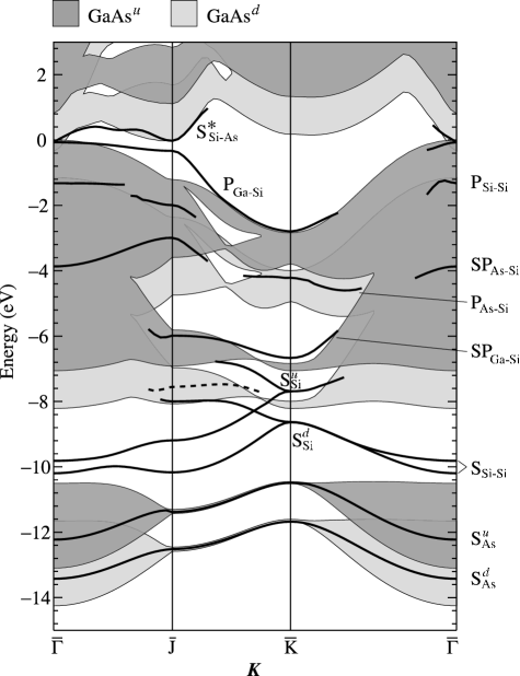
Following the procedure outlined in the previous section, we have calculated the interface states of the Si/GaAs (110) heterojunction. The result is displayed in Fig. 1, where we have represented the dispersion of the states along the principal lines of the irreducible wedge of the two-dimensional Brillouin zone (2DBZ), together with the two bulk PBS’s. The calculated VBO of the Si/GaAs (110) heterojunction (without spin-orbit and self-energy corrections) used for the alignment of the bulk PBS’s is 0.14 eV (Si higher). The high-symmetry points of the 2DBZ are , , , and , in units of ( is the GaAs lattice constant).
The isolated (110) interface has a reflection symmetrykoster ( is the growth direction and is the direction perpendicular to the Si–Si or Ga–As nearest-neighbor zigzag chains in the (110) atomic planes). However, since we have two interfaces per supercell an additional (fictitious) reflection symmetry induces non-degenerate pairs of symmetric and antisymmetric (by reflection) states in the quasi 2DBZ of the supercell (the symmetry group of the supercell is ). With the supercell employed, though, the energy difference between the above pairs is about meV throughout the BZ, thus indicating a small interaction between the two interfaces.
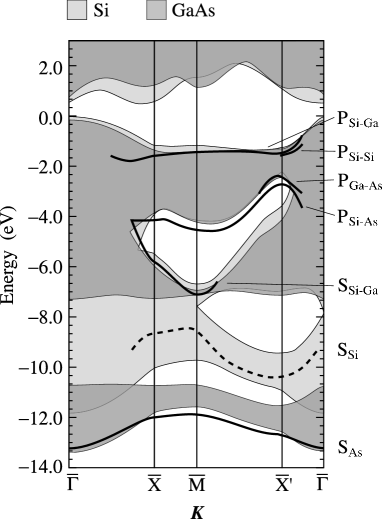
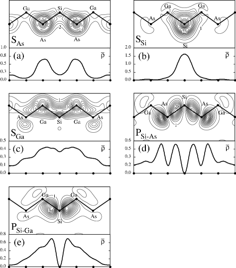
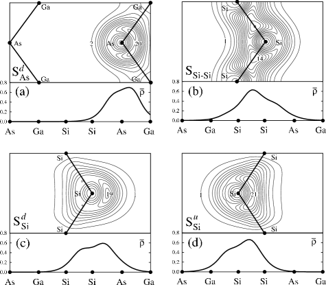
Beginning from the lowest energies, we find a complete band of localized states below (or at the edge of) the bulk PBS of the valence band of GaAs; the probability density of the state at the point of the 2DBZ is shown in Fig. 2(a). These states (S in Fig. 1) derive from the states of the As atoms adjacent to the interface. The localization of these states results from the more attractive ionic potential of Si relative to Ga, which lowers the energy of the As- states at the interface with respect to those in bulk GaAs. This is consistent with the relative strengths of the atomic potentials, which obey the inequality Ga Si As, and leads to the following expected attractiveness of the potential in the interfacial bonding regions: Si–Ga Si–Si Ga–As Si–As. We note that similar localized S states were reported by Pickett et al.pickett for the Ge/GaAs (110) interface.
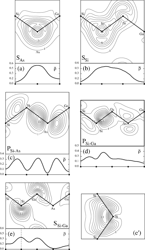
Moving upwards in energy we find a second band of states which have a maximum probability density on the first Si bilayer from the interface (S states, dashed line in Fig. 1). These states are in the energy region of the Si PBS only, and show a small coupling with the Si continuum. Inspection of the probability density of these states, shown in Fig. 2(b), indicates that they derive predominantly from the atomic -states of Si atoms in the second and first layer from the interface. The authors of Ref. pickett, have found analogous resonant states in the case of the Ge/GaAs (110) interface.
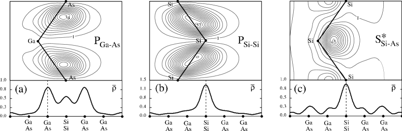
The band in the to eV energy range along the – line corresponds to states related to Si and Ga atoms at the interface (we called them S states). The probability density of one of these states at is displayed in two different planes, perpendicular and parallel to the interface, in Figs. 2(e) and (e’), respectively. Such states contain a large component, and also a non-negligible contribution, of the Si and Ga atoms at the interface, and exhibit a strong antibonding character. They are pushed away from the Si–Ga bonding region into the more attractive Si–Si and Ga–As antibonding regions. We note that at the Ge/GaAs (110) interface, the corresponding states were found to have a dominant contribution from the Ga atom,pickett which is not the case here. We attribute this mainly to strain. Strain pushes the Si states upwards in energy, giving rise to a stronger interaction with the Ga states, and hence to a more significant contribution of the group-IV atom to the antibonding-like interface state (this will become more clear from the study of the ultrathin Si (110) layers in the following sections).
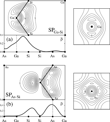
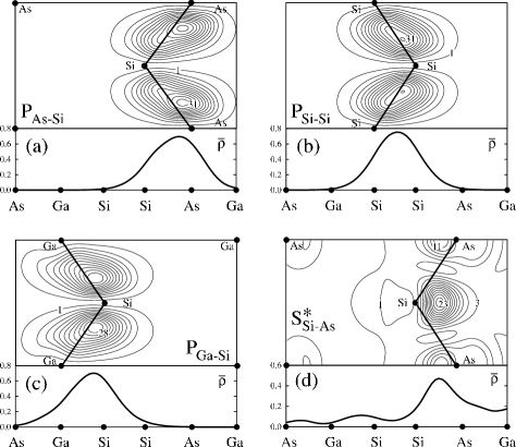
The states of the next two bands that extend in the –– region (P and P) originate from states of the Si atoms at the interface and from states of the interface As and Ga atoms, respectively (see Fig. 2(c) and (d)), which form bonding orbitals across the interface. For the localization of the P states, the same considerations as for the S states are valid. As far as the P states are concerned, we note that due to the repulsive ionic potential in the Si–Ga bonding region (with respect to the potential in the Ga–As or Si–Si regions), these states are pushed at the edge of (or at a higher energy than) the GaAs PBS.
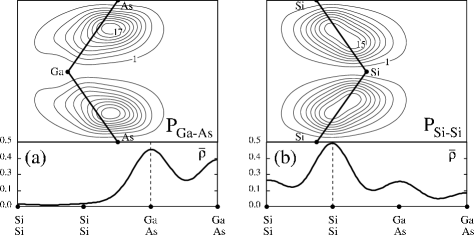
The remaining two types of state (P and P in Fig. 1) are found only in the neighborhood of the point, and have their maximum probability density either on the GaAs (110) plane (P) or on the Si (110) plane (P) adjacent to the interface (see Fig. 3). These states correspond essentially to As–Ga (Si–Si) bonding orbitals within the nearest-neighbor zigzag chains of the (110) plane. We note that the point corresponds to a zone-edge vector perpendicular to the chains. In a tight-binding description,harris this gives rise to a phase in the Bloch functions that leaves the sign of the orbitals of second nearest neighbor atoms in the chain unchanged, but reverses the sign of the atomic-like orbitals in adjacent chains within the (110) plane. This leads to an antibonding configuration between the chains, but allows the formation of nearest-neighbor bonding orbitals within the chain, as seen in Fig. 3. Finally, the fact that the P (P) states are lower (higher) in energy than the P (P) states can be explained by the more attractive ionic potential of Si as compared to Ga.
IV States induced by one Si (110) monolayer in GaAs
Let us return to the S states and also to the S states of the Si/GaAs (110) heterojunction. Their formation and atomic character can be better understood if only few layers of Si are introduced in bulk GaAs. Indeed, the bulk PBS of Si is no longer present, which enhances the localization of some of the Si induced states. We note that some of the states of the Si/GaAs interface are bound to be present also in the ultra-thin layer limit. In particular, all As and Ga-derived states cannot disappear since they essentially originate from GaAs band-edge features. We will see here and in the next section that actually most of the interface states of the fully developed Si/GaAs (110) heterojunction can be traced down to the ML limit.
In Fig. 4 we have plotted the states induced by 1 ML of Si in the GaAs (110) homojunction, together with the GaAs PBS. The layer-induced states have been calculated at . However, the miniband width along is negligible given the thickness of the GaAs slab employed in the present study. We have aligned the supercell states with the bulk GaAs PBS using the calculated shift of the macroscopic average of the electrostatic potential in GaAs relative to its mean value in the supercell. The group symmetry is , and the space group is symmorphic. Thus, all points and lines in the 2DBZ belong to one-dimensional irreducible representations, and no additional degeneracy is introduced by time reversal symmetry.
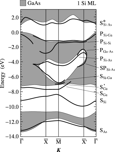
An S band is still present in Fig. 4 at approximately the same energy as in the interface case. This band derives from the states of the As atoms adjacent to the Si layer that form symmetric states under the reflection (see Fig. 5(a)). The antisymmetric counterpart is found as a broad resonance (not shown in Fig. 4) in the PBS of the bulk valence band of GaAs. Conversely, a Si-related band appears at about eV at , whose dispersion from to , to , and to is similar to that of the S interface state. Again, this band corresponds to symmetric states with respect to . The probability density of one of these states (S at ) is displayed in Fig. 5(b). The probability density is predominantly on the Si atoms sitting on the anion sites in the continuation of the zincblende lattice, but also reveals some bonding character with the nearest-neighbor Ga and Si atoms. Considering the Si layer as a perturbation to bulk GaAs,KoSl54 ; withkurt these states separate from the GaAs band and move up in energy, because of the repulsive on-site potential associated with the Si As substitutions. We note that because these localized states have their probability density mostly on the anion sites, within the Si (110) layer at the interface, they are qualitatively different from the Si bulk states present at similar energies in Fig. 1; the latter states derive from Si atomic orbitals with identical weight on the two Si sublattice sites. The former states can thus give rise to Fano resonances when they interact with the continuum of bulk Si states, in the fully developed Si/GaAs (110) heterojunction. The latter interaction generates bonding features between the Si atoms sitting on anion sites, in the layer closest to GaAs, and the Si atoms sitting on cation sites, in the neighboring layer on the Si side. This, in turn, pushes the probability density of the S state towards the second Si layer, when the heterojunction is formed.
In the neighborhood of the point, along the ––– path in Fig. 4, the S state couples with the symmetric state we labeled S. The latter state derive mainly from the states of the Ga atoms adjacent to the Si layer (its probability density at is shown in Fig. 5(c)). Consistent with the ordering expected from the corresponding levels in the isolated atoms, the energy positions of the localized states of As, Si, and Ga are found in ascending order. The state labeled S, observed at , is the antisymmetric counterpart of the S state (see Fig. 6(c)), while the symmetric S state, found in the lower part of the GaAs stomach gap, has mixed Si and Ga (with some ) atomic character (see Fig. 6(b)).
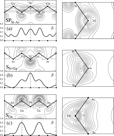
Another state (also symmetric under the reflection) is observed in the lower part of the GaAs stomach gap, but only near the point (SP). The latter state is not present in the fully developed Si/GaAs (110) heterojunction, and originates mainly from states of the As atoms adjacent to the Si layer and hybrids of the neighboring Si atoms (see Fig. 6(a)). The P (P) state derives from the anti-symmetric combination of the P (P) interface states on each side of the Si layer (see Figs. 5 and 2). The P and P states are symmetric states, which also derive from their interface counterparts (see Figs. 7 and 3).
Finally, we find a well localized conduction state in part of the GaAs fundamental bandgap (S in Fig. 4) which does not exist in the fully developed Si/GaAs (110) heterojunction. The latter state is an antibonding Si–As state with strong -hybrid character from the Si atoms occupying the cation sites within the (110) layer (see Fig. 7(c)). This state is essentially a quantum-well state in its early stage formation. At larger Si intralayer thickness, the localization of this state, at specific points of the 2DBZ, will be due to the conduction band offset of Si in GaAs (i.e., the quantum-well potential, within an effective-mass description). The S state is present within the GaAs bandgap in a large portion of the 2DBZ. Yet, we recall that the GaAs and Si bandgaps are affected by an error within the LDA-DFT approach, which may affect also the existence of the S state. The calculated GaAs LDA (direct) gap is 0.9 eV, while the experimental valuelan is 1.52 eV ( eV correction), and the Si LDA gap is about 0.5 eV to be compared to the experimental valuelan of 1.17 eV ( eV correction). The gap corrections, however, turn out to be similar for Si and GaAs; also, the corrections are expected to be rather rigid shifts throughout the BZ. We therefore do not expect drastic changes in the alignment of the Si and GaAs conduction bands. To have an estimate of the conduction offset controlling the localization of the most bound S states, we should compare the X (indirect) gap of GaAs (its calculated value is 1.4 eV; the experimental valuelan is 2.18 eV) with the corresponding gap of Si. Taking into account the 0.14 eV VBO, we thus conclude that the states near are bound by a conduction offset of about 0.87 eV, to be compared to the theoretical offset of 0.76 eV. This gives us confidence in the existence of the S states also in the actual quasiparticle interface spectrum.
V States induced by two Si (110) monolayers in GaAs
We end this study of non-polar (110)-oriented structures with the case of 2 MLs of Si in GaAs. This case is intermediate between the fully developed interface and the single Si impurity-sheet perturbation. The point group symmetry of the 2 Si MLs in GaAs contains the reflection operations , , and a twofold rotation around the axis. The point group is , and the space group is non-symmorphic with fractional translation (in lattice units). Since our calculations do not take into account the non-scalar spin-orbit interaction, no additional degeneracy is imposed along the – and – lines by time reversal symmetry. We thus expect along these lines pairs of symmetric and antisymmetric states for each atomic-orbital derived state. Conversely, the representations of the groups of and belong to the two-dimensional irreducible representation , and that of to the two-dimensional representation of , for which an additional degeneracy is present.
We plot in Fig. 8 the states induced by 2 MLs of Si in bulk GaAs. We have aligned the localized states and resonances with the GaAs PBS only, as in the 1 ML case. In Fig. 8, we distinguished the symmetric (by reflection) from the antisymmetric states, which have a small probability density between the adjacent Si layers. Comparing the results for the 2 Si MLs with those obtained for 1 Si ML and the fully developed interface, we see that the connection between the states of 1 ML and of the interface is made by the symmetric and antisymmetric states of the 2 MLs structure, which eventually become degenerate for thicker Si layers. We note that the S’ and SP states are no longer present already at 2 Si MLs coverage. Yet, we find a well localized S state in a relatively large portion of the 2DBZ. This state is localized in regions of the 2DBZ, which more closely correspond to the regions exhibiting a large Si/GaAs conduction band offset, as compared to the 1 ML case. Following the considerations given for the 1 ML case, this indicates that we are in a situation in which the quantum well potential is nearly established, with a potential strength that is becoming similar to the conduction-band offset between Si and GaAs.
VI States induced by a Si (100) bilayer in GaAs
The situation is more complicated for (100)- than for (110)-oriented heterovalent heterostructures, because of the polarity of the [100] growth direction. We mentioned in the Introduction that the fully developed abrupt Si/GaAs (100) heterojunction is thermodynamically unstable, as it is macroscopically charged. Similarly, an abrupt Si (100) monolayer in GaAs is also macroscopically charged and thermodynamically unstable. An abrupt Si (100) bilayer, instead, gives rise to a dipole, which is the lowest-order multipole which does not generate a long-range electric field and is hence, in principle, energetically acceptable. The dipole layer also corresponds to the highest-order multipole which can induce a change in the band alignment, and is therefore of possible interest for interfacial band engineering. Here we thus focus on the bilayer case. Some caution, however, is in order when comparing to experiment. Although photoemission and internal photoemission studies have reported some changes in the band alignment in the presence of Si interlayers,sorba ; titti1 ; marsi this effect was found to saturate at Si coverages of about 0.5 ML, and to decrease in amplitude at higher coverages. This has been interpretedmariapert as an indication of significant deviations from a Si bilayer distribution above 0.5 ML, due to atomic interdiffusion. It should be stressed, however, that the positions of the Si atoms are unknown in any case, and it is only speculatively that one may assume a dipole layer distribution, even at low coverage. We thus consider the simplest possible case of 2 MLs of Si in an abrupt bilayer configuration, and we will end this section with some considerations on the trends one may expect for bilayers with lower Si nominal concentration. Although 2 MLs of Si in a bilayer geometry is a structure which has not been produced experimentally so far, the study of this system is interesting in itself to establish a relationship between the interface states of the (110) and (100) heterostructures. We also want to show that intrinsic scattering centers can exist in the (100) systems, even in an abrupt, defect-free heterostructure.
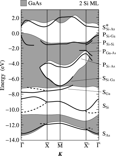
In Fig. 9, we show the dispersion of the states induced by 2 MLs of Si in the (100) GaAs homojunction. The PBSs of the two GaAs bulks on each side of the junction (GaAsu, GaAsd) are rigidly shifted one with respect to the other by eV, which is the calculated VBO of the relaxed heterostructure. In the LDA framework, the system is metallic near . However, this would not be the case if the experimental gap of GaAs had been used. We note that the zone center has a very small weight in the BZ integrations (our grid actually does not include the point). The charge transfer generated by the small valence-conduction band overlap at has therefore a negligible influence on the band alignment (the computed potential lineup agrees within 0.1 eV with the prediction of the linear-response model of Ref. mariapert, ). The point group symmetry of the isolated bilayer in GaAs is . Since we have two Si bilayers in the supercell, rotated by one with respect to the other around the twofold axis, a higher symmetry is present in the superlattice. The irreducible part of the 2DBZ of our calculation is thus one half of that of the isolated bilayer, and each point in the irreducible BZ includes states of both bilayers. However no additional degeneracy is induced by time reversal symmetry. The bands are shown along the high symmetry lines connecting , and (in units of , where is the GaAs lattice constant).
Beginning from the lowest energies, we recover the As-related -state band. In the present case, pairs of localized states separated by appear, which correspond to As on the upper and lower (S in Fig. 10(a)) energy side of the heterostructure. We observe three different types of localized Si -like states in the Si (100) bilayer structure: one derives mainly from Si atoms sitting on the Ga sites (S, see Fig. 10(c)), the second one is associated mostly with Si atoms on the As sites (S, see Fig. 10(d)), while the third one involves Si atoms from both cation and anion sites (S in Fig. 10(b)), and shows strong Si–Si bonding features. The first two types of states are found essentially around the zone edge point, whereas the S states are observed in the remaining part of the 2DBZ. The character of the S states changes progressively along the – direction, and matches the character of the S and S states at .
The Ga-related localized state of the (110) GaAs/1 Si ML/GaAs heterostructure is found as a resonance in the present case (dashed line in Fig. 9). Conversely, we find well-localized states which derive from interacting Ga and Si states (SP in Fig. 11(a)). We also find an SP state, which results from the interaction between As hybrids and Si orbitals (SP in Fig. 11(b)). The in-plane (110) P interface state is no longer present, as one might have expected since the planes of Ga–As zigzag chains are now perpendicular to the interface. The P state, instead, is found as a bilayer state, oriented in the (100) direction (see Fig. 12(b)). We note that the P state appears only near the valence edge of the GaAsd PBS, along the – line. The state originating from the interaction between the states of As and Si (P in Fig. 12(a)) is found near the zone-edge point, and is a resonance in the GaAsd PBS.
Finally, we also report two states which are present in the main PBS gap (apart from the metallic region near ). The first one is a Ga–Si bonding state resulting from the interaction between the states of Ga and Si (P, see Fig. 12(c)) at the GaAsu/Si junction. The second one is a Si–As antibonding state deriving from hybrids of the Si and (to a lesser extent) of the As atoms (S, see Fig. 12(d)) at the Si/GaAsd junction. Both states, and in particular the P state, exhibit a relatively weak dispersion along the – line, leading to an enhanced DOS near the GaAsu valence-band edge (P) and the GaAsd conduction-band edge (S).
In the presence of only one of the two GaAsu/Si and Si/GaAsd interfaces, we expect the resulting P or S states to be within the GaAs optical gap near . This is confirmed by ab initio computations we performed for related engineered systems, namely abrupt Al/6 Si MLs/GaAs (100) metal-semiconductor structures with either an As- or a Ga-GaAs (100) termination at the polar Si/GaAs interface.berthod99 The dispersion of the corresponding S and P states is shown in Fig. 13, along the high symmetry direction of the 2DBZ, together with the probability density of these states. Although the As- and Ga-terminated Al/6 Si MLs/GaAs (100) metal/semiconductor structures incorporate only one of the two types of charged Si/GaAs (100) interfaces each, they exhibit no macroscopic electric field in the bulk semiconductor (GaAs)—because of the presence of the metal—and display either a GaAsd energy-shifted bulk (in the As-terminated junction) or a GaAsu energy-shifted bulk (in the Ga-terminated junction). Also, the thickness of the Si (6 Si monolayers pseudomorphically strained to GaAs) insures negligible interaction between the continuum of Al bulk states, on one side of the interlayer, and the resonant S or P Si/GaAs-interface states, on the other side of the interlayer. In these conditions, the As-terminated (Ga-terminated) junction gives rise (see Fig. 13) to a band of the S (P) Si/GaAs interface states which has a dispersion similar to that of Fig. 9 within the GaAs PBSs bandgap, but with an energy at which is well within the gap, namely eV below ( eV above) the conduction- (valence-) band edge of the GaAs PBS.
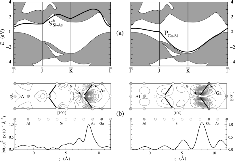
The S and P states that we find at the abrupt As-terminated and Ga-terminated Si/GaAs (100) interfaces, respectively, are the (100) analogues of the S and P states that we observed in the non-polar GaAs/Si/GaAs (110) heterostructures. However, contrary to the case of the globally neutral Si/GaAs (110) junction, at the As- terminated Si/GaAs (100) interface, the attractive potential created by the globally positive excess ionic charge of the As–Si donor bonds is sufficiently strong to pull down S conduction states within the GaAs fundamental gap. Similarly, the potential created by the globally negative ionic charge of the Ga–Si acceptor bonds is able to push up P states from the valence band into the GaAs gap. Hence, the S (P) states become potential scattering centers at the polar As-terminated (Ga-terminated) Si/GaAs (100) heterojunction.
As mentioned before, Si may be confined in a bilayer geometry only at nominal coverages lower than or equal to 0.5 ML. We have therefore also investigated what happens to the S and P states when the Si coverage is reduced to 0.5 ML. We have considered two different ordered GaAs/Si/GaAs () interlayer atomic configurations corresponding each to one Si Ga and one Si As atomic substitution per () surface-unit cell within the GaAs bilayer. In the first configuration, the pair of Si atoms sit on adjacent Ga-As sites, so that each Si atom has three As or three Ga nearest neighbors and one Si nearest neighbor (configuration A), whereas in the second configuration each Si atom has four As or four Ga nearest neighbors, and no Si nearest neighbor (configuration B).noteAB
In both A and B configurations, we find that the S (P) states associated with the Si–As (Si–Ga) donor (acceptor) bonds become resonances at . The energy positions of the resonances depend somewhat on the Si arrangement. The S resonance is located at eV from the conduction band edge in the A configuration, and at eV from the same edge in the B configuration. The P resonance remains, instead, a near-band edge resonance (within 0.1 eV from the valence band edge) in both cases. We note that, in both cases, the conduction resonance gives rise to a stronger DOS feature than the valence resonance, due to the lower density of bulk states present near the conduction edge. The conduction resonance may be responsible for a peculiar feature observed in internal photoemission experiments by dell’Orto et al.titti The associated increased DOS at is indeed detectable, in principle, by transport measurements.titti
VII Koster-Slater model for the interface-state problem
The ab initio calculations of the preceding sections have provided us with the energy position and atomic-like character of various states localized at the Si/GaAs interface. However, it is not simple to extract from the full-fledged ab initio calculations a general understanding of the mechanisms of interface-state formation. For example, it is evident from Fig. 1 that except for the S states which form a complete band along the high-symmetry lines, the other states appear only along specific lines or near specific points of the 2DBZ. This is a common feature observed for many different interfaces studied in the literature. In this section, we thus try to rationalize the above results based on a more general, yet simplified description, that contains the main physical ingredients of the problem. Specifically, one would like such a model to include the effects of (i) the strength and sign of the local potential at the interface generated by the different chemical nature of the interface atomic constituents, (ii) the band structures of the two bulk materials, and (iii) the macroscopic lineup of the two bulk band structures across the interface. We report below a simple analytical criterion for the existence of interface states, which explicitly relates the existence of these states to (i), (ii), and (iii). A derivation of the analytical form of this criterion, which is mathematically simple and physically transparent, is also presented. A detailed and rigorous quantum-mechanical derivation, together with the explicit expressions for the microscopic interface-specific terms, is given in Ref. max, .
An interface can be regarded as a perturbation of the bonding structures of two different bulk materials.pollman Also, since for stable interfaces the perturbation involved is neutral and short ranged, we may formulate the problem in terms of few perturbed layers, and thus derive a criterion similar to the one Koster and Slater introduced for deep impurities in semiconductors.KoSl54 Following the authors of Ref. pollman, , we construct the interface as a perturbation of two bulk semiconductors and . We write the unperturbed Hamiltonian as
| (1) |
where and are the Hamiltonians of the two bulk periodic crystals, with standard periodic boundary conditions over layers. The corresponding one-particle Green’s function of the system is
| (2) |
with and the Green’s functions of the Hamiltonians and , respectively. A perturbation (which will be specified below) is then introduced; acts on this system, and in particular couples and , and yields an interface (plus two free surfaces). The total Hamiltonian describing the perturbed system is . A basis set of Wannier functions is assumed in the following discussion. Specifically, as preserves the periodicity in planes parallel to the interface, the basis functions at a given -point in the 2DBZ consists of localized-layer Wannier functionspollman in and , obtained from the Bloch functions of the corresponding bulk with wave-vector projection in the 2DBZ equal to .
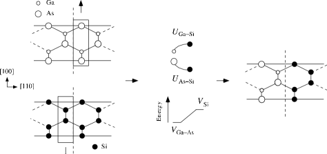
The construction of the interface, and thus of the perturbation , is schematized in Fig. 14. We consider the Si/GaAs (110) interface, and assume for simplicity that the interactions are described by tight-binding nearest-neighbor Hamiltonians. To keep the expressions as simple as possible, we also refer in the following to one band for each bulk semiconductor. The generalization to the multiband case is straightforward.max A layer of atoms of material (e.g., GaAs) and a layer of atoms (Si) are first removed on each side of the interface in bulk space and , respectively. This procedure is analogous to the creation of free surfaces and can be performed in practice by changing the on-site parameters and , which eventually are let go to infinity.pollman Then, the interactions between the atoms of the left-hand side and right-hand side surfaces (Si–Ga and Si–As) are switched on across the interface. These interactions are represented by off-diagonal terms , which are nearest-neighbor tight-binding matrix elements coupling the two interface layers. Finally, the charge transfer at the interface, i.e., the perturbation induced by the interface relative to a superposition of bulk crystal potentials, is added as on-site diagonal matrix elements and for the semiconductor interface layer and , respectively. Since these perturbations are measured with respect to the average electrostatic potential of the corresponding bulks, the lineup is introduced in the Green’s functions of the bulks. If we assume that the removal procedure described above has been performed, the only relevant block of the matrix is
| (3) |
where all elements are scalars in the one-band model. The condition for having bound states can then be derived from the determinantal equationeconomou
| (4) |
and reads
| (5) |
If the zero of energy is fixed at the top of the valence band , the Green’s functions are:
| (6) |
and
| (7) |
The condition (5) tends to the usual Koster-Slater relation, , for deep impurities ( being the potential perturbation induced by the impurity in the host described by ) when only one semiconductor and on-site interactions are retained. Given the linear relation, , between the Green’s function of a bulk and the corresponding electronic density of states (DOS), , we find from Eq. (5) that, for a given set of parameters (, and ), the existence of bound states and resonances depends on: (i) the strength of the DOS of each bulk band with respect to the corresponding on-site parameter , and (ii) the amplitude of the product of the DOS’s of the two bulk bands with respect to the interface coupling parameter . Localized states may appear above/below the bulk bands according not only to the strength of the on-site terms and at the interface, but also to the relative strength of these terms and the coupling terms .max In fact, when , can push states both above and below the bulk bands. It should be noted, however, that when the band offset is non-vanishing, even in a one-dimensional model, the on-site perturbations generated by the interface may induce resonances rather than bound states. This is in contrast to the case of deep impurities, where a state is always bound in one dimension (for local potentials).
With the help of Eq. (5), we can now try to identify the regions and points of the 2DBZ where interface states are most likely to appear. In view of the relationship between Green’s function and DOS, we have examined the DOS of both Si and GaAs bulks, for a given point of the (110) 2DBZ, integrated along a line in -space parallel to the growth direction. The result is plotted in Fig. 15 for the four high-symmetry points of the (110) 2DBZ. The DOS has been calculated using tetragonal (properly strained) supercells of 4 atoms oriented along the (110) direction for both bulks. For each point in the 2DBZ we sampled the (110) direction with 26 -points distributed on a uniform grid. A Gaussian broadening of 0.1 eV was used. We have employed the same procedure as in the previous section to align the DOS’s of the two bulks.

The DOS of GaAs is a sharp feature, well separated from the Si bands at , , and . The localized S state is induced thus by an on-site perturbation. The on-site potential is attractive,max due to the attractive potential of the nearest Si atoms, and is responsible for the existence of this state. The S states originate mainly from both the Si and GaAs peaks located at about eV and eV in the and DOS’s spectra, respectively. These edges are associated with Si (GaAs) electronic states that contain an important component, together with a non-negligible contribution, from the Si (Ga) atoms. The on-site and matrix elements of adjacent Ga and Si atoms are repulsive.max However, contrary to the case of the As states, the Si and GaAs edges are separated by less than 1 eV, and the term also contributes to the formation of the S states. At and , instead, no comparable DOS features are detected at similar energies.
At , two pronounced and strongly overlapping Si and GaAs DOS features are visible: with band edges at about eV and eV. The lower edges contribute predominantly to the P and P states, and the upper ones to the P and P states. However, only the P and P states can be followed along the 2DBZ up to the point. The strong overlap near the band edges make the contribution of the term important, as evidenced by the mixed Si-GaAs nature of the resulting interface states. These states are localized by the attractive (repulsive) ionic potential in the Si–As (Si–Ga) bonding region.max At the point, no bound state is present in the fundamental gap. This is due to the attractive character of the and matrix elements,max and to the finite value of the band offset. The off-diagonal term has thus not enough strength to push a state in the gap; we note that the situation changes, instead, at the polar, negatively charged Ga-terminated Si/GaAs (100) interface, where the repulsive potential induced by the negative charge pushes the P state within the GaAs bandgap. Similar considerations apply to other abrupt interfaces studied in the literature,baraf ; pickett ; pollman ; saito ; wang ; laref ; apl2001 giving us confidence in the soundness of the above model description. We also note that estimates for the interface-bonding parameters may be obtained from relatively simple models, such as the tight-binding approach of Ref. pollman, .
VIII summary and conclusions
Using an ab initio pseudopotential approach, we have studied the states induced by thin Si interlayers in abrupt GaAs/Si/GaAs (110) and (100) heterostructures. We have also investigated the interface states of the fully developed Si/GaAs (110) heterojunction and resonant Si/GaAs (100) interface states occurring within the GaAs bandgap in Al/6 Si MLs/GaAs (100) heterojunctions. We have examined the bonding properties and atomic character of these various states, and their possible connections.
The results reveal interesting common features between localized states and resonances in structures with different interface orientations and, for a given orientation, between states localized by 1 or 2 Si monolayers and the interface states of the fully developed Si/GaAs junction. By studying the evolution of the resonances and localized states with Si-interlayer thickness, we were able to explain the origin of Si-related resonant interface states occurring in the fully developed Si/GaAs (110) junction. The ab initio results also indicated that most of the localized states of the Si/GaAs (110) interface persist up to 2 and even 1 monolayer Si-interlayer coverage. Moreover, the most striking valence- (conduction-) near-band edge states found in the GaAs/2 Si MLs/GaAs (100) heterostructure were also shown to originate from localized As–Si donor-bond (Ga–Si acceptor-bond) states of the fully developed As-terminated (Ga-terminated) Si/GaAs (100) interface.
In order to gain further insight into the mechanism of formation of interface states, we have presented a Koster-Slater type model developed for the interface-state problem. A simple analytical criterion for the existence of interface states [Eq. (5)] has been derived, which allows us to predict the existence and/or energy of interface states from the DOS structure of the constituent materials and from some interface bonding parameters.max With this model, we were able to explain the different type of localized states obtained from the ab initio calculations for the GaAs/Si interface, and account for their energy position and location within the Brillouin zone. More generally, this model is expected to be useful to predict trends due to changes in the interface atomic structure (e.g., due to atomic intermixingmax ) or in the electronic band structure of the bulk materials (e.g., due to alloying or different polytypesapl2001 ).
Acknowledgements.
We acknowledge the hospitality and support of the Ecole Polytechnique Fédérale of Lausanne where most of this work has been performed while two of us (MD and CB) were completing their PhD thesis.References
- (1) See e.g., A. Franciosi and C. G. Van de Walle, Surf. Sci. Rep. 25, 1 (1996); and references therein.
- (2) F. Capasso, Science 235, 172 (1987).
- (3) W. A. Harrison, E. A. Kraut, J. R. Waldrop, and R. W. Grant, Phys. Rev. B 18, 4402 (1978).
- (4) M. Peressi, S. Baroni, R. Resta, and A. Baldereschi, Phys. Rev. B 43, 7347 (1991).
- (5) S. De Franceschi, F. Altomare, F. Beltram, M. Lazzarino, L. Sorba, and A. Franciosi, J. Appl. Phys. 84, 4637 (1998).
- (6) M. Moreno, H. Yang, M. Höricke, M. Alonso, J. A. Martín-Gago, R. Hey, K. Horn, J. L. Sacedón, K. H. Ploog, Phys. Rev. B 57, 12314 (1998); M. Moreno, J. L. Sacedón, M. Alonso, M. Höricke, R. Hey, J. Avila, M. C. Asensio, K. Horn, K. H. Ploog, Phys. Rev. B 58, 13767 (1998).
- (7) L. Sorba, G. Bratina, A. Antonini, J. F. Walker, M. Mikovic, G. Ceccone, and A. Franciosi, Phys. Rev. B 43, 2450 (1991); G. Bratina, L. Sorba, A. Antonini, G. Biasiol, and A. Franciosi, Phys. Rev. B 45, 4528 (1992).
- (8) T. dell’Orto, J. Almeida, C. Coluzza, A. Baldereschi, G. Margaritondo, M. Cantile, S. Yildirim, L. Sorba, and A. Franciosi, Appl. Phys. Lett. 64, 2111 (1994).
- (9) M. Marsi, R. Houdré, A. Rudra, M. Ilegems, F. Gozzo, C. Coluzza, and G. Margaritondo, Phys. Rev. B 47, 6455 (1993).
- (10) S. Modesti, D. Furlanetto, M. Piccin. S. Rubini, and A. Franciosi, Appl. Phys. Lett. 82, 1932 (2003).
- (11) G. A. Baraff, J. A. Appelbaum, and D. R. Hamann, Phys. Rev. Lett. 38, 237 (1977); G. A. Baraff, J. A. Appelbaum, and D. R. Hamann, J. Vac. Sci. Technol. 14, 999 (1977).
- (12) W. E. Pickett and M. L. Cohen, Phys. Rev. B 18, 939 (1978); W. E. Pickett, S. G. Louie, and M. L. Cohen, Phys. Rev. B 17, 815 (1978).
- (13) J. Pollmann and S. T. Pantelides, Phys. Rev. B 21 709 (1980).
- (14) T. Saito and T. Ikoma, Phys. Rev. B 45, 1762 (1992).
- (15) L. Zhu, E. Wang, and L. Zhang, Phys. Rev. B 56, 10308 (1997); and references therein.
- (16) A. Laref, H. Aourag, B. Belgoumene, and A. Tadjer, J. Appl. Phys. 94, 5027 (2003).
- (17) M. Peressi, F. Favot, G. Cangiani, and A. Baldereschi, Appl. Phys. Lett. 81, 5171 (2002); and references therein.
- (18) M. Di Ventra, C. Berthod, and N. Binggeli, Phys. Rev. B 62, R10622 (2000).
- (19) D. M. Ceperley and B. J. Alder, Phys. Rev. Lett. 45, 566 (1980).
- (20) N. Troullier and J. L. Martins, Phys. Rev. B 43, 1993 (1991).
- (21) L. Kleinman and D. M. Bylander, Phys Rev Lett. 48, 1425 (1982).
- (22) H. J. Monkhorst and J. P. Pack, Phys. Rev. B 13, 5188 (1976).
- (23) Numerical Data and Functional Relationships in Science and Technology, Landolt-Börnstein, New Series, Vol. 22 pt. a (Springer, 1987).
- (24) See, e.g., M. Peressi and S. Baroni, Phys. Rev. B 49, 7490 (1994).
- (25) C. G. Van de Walle, Phys. Rev. B 39, 1871 (1989).
- (26) We note that localized interface states may exist also within the bulk PBS if their symmetry differs from that of the bulk states. This is, however, relatively unlikely in semiconductor heterojunctions, especially at generic points of the BZ.
- (27) A. Baldereschi, M. Peressi, S. Baroni, and R. Resta, in Proceedings of the International School of Physics “Enrico Fermi” Course CXVII, Semiconductor Superlattices and Interfaces, edited by L. Miglio and A. Stella (Academic, New York, 1993), p. 59.
- (28) M. Peressi, N. Binggeli, and A. Baldereschi, J. Phys. D 31, 1273 (1998).
- (29) G. F. Koster, J. O. Dimmock, R. G. Wheeler, and H. Statz, Properties of the Thirty-two Point Groups (MIT Press, Cambridge, 1963).
- (30) W. A. Harrison, Electronic Structure and the Properties of Solids (W. H. Freeman and Company, San Francisco, 1980), ch. 3.
- (31) G. F. Koster and J. C. Slater , Phys. Rev. 96, 1208 (1954).
- (32) M. Di Ventra and K. A. Mäder, Phys. Rev. B 55, 13148 (1997).
- (33) C. Berthod, Ph.D. thesis, EPFL (1999).
- (34) Configuration A is found to be lower in energy by eV per Si atom than configuration B.
- (35) T. dell’Orto, M. Di Ventra, J. Almeida, C. Coluzza, and G. Margaritondo, Phys. Rev. B, 52 R2265, (1995).
- (36) E. N. Economou, Green’s Functions in Quantum Physics, (Springer, 1979).
- (37) M. Di Ventra, Appl. Phys. Lett. 79, 2402 (2001).