Ambipolar Cu- and Fe-Phthalocyanine single-crystal field-effect transistors
Abstract
We report the observation of ambipolar transport in field-effect transistors fabricated on single crystals of Copper- and Iron-Phthalocyanine, using gold as a high work-function metal for the fabrication of source and drain electrodes. In these devices, the room-temperature mobility of holes reaches 0.3 cm2/Vs in both materials. The highest mobility for electrons is observed for Iron-Phthalocyanines and is approximately one order of magnitude lower. Our measurements indicate that these values are limited by extrinsic contact effects due to the transistor fabrication and suggest that considerably higher values for the electron and hole mobility can be achieved in these materials.
pacs:
72.80.Le, 73.40.Qv, 73.61.PhMost of the organic transistors that have been fabricated until now have shown unipolar conduction, i.e. they function for only one polarity of the gate voltage Dimitrakopoulos02 . Only very recently, ambipolar device operation has been reported in Field-Effect Transistors (FETs) based on a few different single-component note1 organic molecular semiconductors Meijer03 ; Chesterfield03 ; Kunugi04 ; Yasuda05 . Some of these ambipolar devices have been used to realize inverter circuits that demonstrate the possibility of implementing CMOS technology Anthopoulos04 . Since CMOS technology is the most efficient strategy towards the fabrication of integrated circuits with better noise margins (i.e. insensitivity to the spread in the parameters of the individual devices) and consuming less power Meijer03 ; Crone00 , this represents a considerable step forward in the field of plastic electronics. Particularly important is that the implementation of plastic CMOS integrated circuits can be realized using a single molecular semiconductor rather than two different materials, since this has the potential to considerably simplify the device fabrication processes. So far, however, the number of single-component molecular semiconductors for which ambipolar FET operation has been reported is rather limited.
In this paper we report the investigation of field-effect transistors fabricated on single-crystals of Copper- and Iron-Phthalocynanines (Cu- and Fe-Pc’s), using gold as a high work function material for the fabrication of the source and drain electrodes. Electrical measurements performed in high-vacuum demonstrate the occurrence of both hole and electron conduction. From the electrical characteristics of these first organic single-crystal FET we extract room-temperature mobility values for holes reaching 0.3 cm2/Vs for both materials. The typical electron mobility values are different for FePc and CuPc. In FePc the electron mobility reaches 0.03 cm2/Vs whereas, in CuPc it is typically lower than 10-3 cm2/Vs. These values are limited by device non-idealities of extrinsic origin, which originate from difficulties in the FET assembly and which clearly manifest themselves in the transistor electrical characteristics. We expect that, upon improving the device assembly procedure, considerably higher electron and hole mobility can be reached in Copper- and Iron-Phthalocyanine ambipolar FETs.
The devices used in our studies have been fabricated by means of electrostatic bonding of very thin (m thick), flexible crystals to a substrate onto which the FET circuitry had been previously fabricated. The details of the technique and of the crystal growth are similar to those used for the fabrication of tetracene and rubrene single-crystal FETs DeBoer04 . From X-ray diffraction measurements we find that the structure of both CuPc and FePc crystals, which were grown from vapor phase Laudise98 , is the known -form Gould96 . All crystals used in this work are needle-shaped and their long direction is aligned along the crystalline -axis.
Contrary to what happens for rubrene or tetracene single crystals DeBoer04 , for which the width of very thin crystals can easily exceed 1 mm, we have found that the width of thin and flexible CuPc and FePc single crystals that are capable of bonding to rigid substrates is typically smaller than 100 m (see inset in Fig. 1). In addition, very thin crystals are fragile and easily crack along the crystalline -axis. These properties of the CuPc and FePc crystals substantially increase the difficulties involved in the crystal handling and in the device assembly, often resulting in damage to the crystal or in a poorer adhesion of the crystals to the substrate and to the contacts. In spite of these difficulties, we have successfully fabricated and measured a large number of FETs on FePc and CuPc. All of the devices fabricated using FePc and approximately half of the devices fabricated using CuPc exhibited ambipolar transport.
The electrical characterization of the devices has been performed in a vacuum chamber (pressure mbar) and in the dark. All the data shown here were taken in a two terminal configuration, using a HP4156 parameter analyzer, at room temperature. We found that heating of the device in-situ up to a temperature of 450 K for a period of several hours results in a clear improvement of the electrical characteristics (e.g. reduction of hysteresis) and in a substantial enhancement of the electron current. This behavior has been observed before and is attributed to thermally-induced de-sorption of oxygen and water vapor present in the crystals Meijer03 ; DeLeeuw97 and acting as traps for electrons Zeis05 . We have also noticed that heating the device for much longer periods (days) results in further smaller improvements of the transistor characteristics, e.g. a factor-of-two enhancement of the mobility of both electrons and holes. This phenomenon is likely to originate from the lowering of the contact resistance due to a better adhesion between crystal and electrodes, or from the annealing of structural defects.
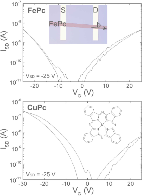
Fig. 1 shows logarithmic plots of the source-drain current measured as a function of gate voltage , for a fixed value of source-drain voltage , in a FePc and in a CuPc device. It is apparent that the measured current increases with increasing for both negative and positive polarity. This demonstrates the occurrence of ambipolar transport in these materials. In general, we observe that at large gate voltage, and under comparable biasing conditions, the electron current is normally lower than the hole current (approximately one-to-two orders of magnitude).
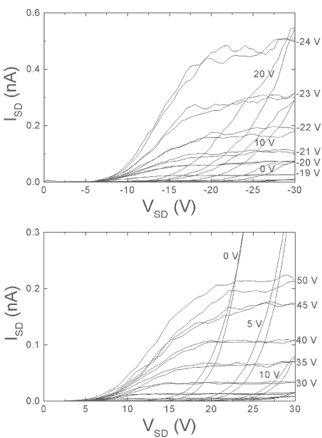
The transistor characteristics of a FePc device measured by sweeping the source-drain voltage at different, fixed values of are shown in Fig. 2. These measurements illustrate that the typical transistor behavior is observed for both negative and positive gate voltage and confirm the occurrence of ambipolar operation. Overall, the observed behavior is very similar to that exhibited by recently reported, ambipolar organic FETs, realized on thin-films of different organic semiconductors Meijer03 .
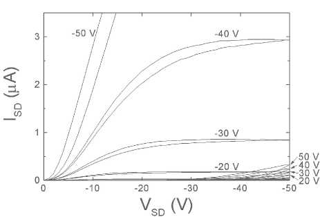
The mobility of electrons and holes in different FETs has been estimated at room temperature from the linear regime of the device operation. We find a rather large spread in the measured mobility values. For FePc hole and electron mobilities were found in the range cm2/Vs and cm2/Vs, respectively. For CuPc, the measured values for the hole mobility are in the same range as in FePc, whereas the values for electron mobility are typically lower ( cm2/Vs). We attribute the large spread of mobility to the presence of contact effects that are visible in the electrical characteristics of even the best devices (see Fig. 3). In this regard, the electrical behavior of these FePc and CuPc FETs is different from that observed in tetracene DeBoer03 and rubrene Podzorov03 ; Podzorov04 ; Stassen04 single-crystal FET, which exhibit a considerably smaller spread in mobility values. Nevertheless, the best mobility values that we have found for both electron and holes already compare well to the highest mobility values reported for ambipolar thin-film organic FETs.
Since contact limitations in FePc and CuPc single-crystal FETs are visible for both holes and electrons even though the work function of gold is ideally aligned to the HOMO of the molecules, we conclude that these contact effects are largely of extrinsic origin, due to the FET assembly process (e.g. imperfect adhesion of the crystal onto the metal contact). Note, however, that whereas the values for the hole mobility are approximately the same for the two different phthalocyanines, the mobility of electrons is systematically higher in FePc than in CuPc. This is consistent with the HOMO-LUMO gap of FePc being smaller than that of CuPc Liao01 , which allows a more efficient electron in injection in FePc than in CuPc. Thus, in short, the data suggest that even though extrinsic contact effects are present and limit the measured value of the hole mobility to 0.3 cm2/Vs, the electron current is also significantly limited by the intrinsic misalignment between the gold work function and the molecular level for electron transport in the material Meijer03 .
In comparing the behavior of our single-crystal FETs with thin-film FETs made with the same materials, it is interesting to note that ambipolar transport in CuPc thin-film transistors has been observed only very recently in devices using Calcium electrodes Yasuda05 . Even though gold contacted CuPc thin-film FETs have been extensively studied in the past Bao96 , ambipolar operation has never been reported in those devices. This suggest that the structural quality of the organic semiconductor (a major difference between thin-film and single-crystal devices) is also a relevant factor for the observation of ambipolar FET operation Zeis05 .
Finally, together with previous experiments on thin-film FETs of different phthalocyanines in which both p- and n-type operation has been observed depending on the atmosphere in which the devices are operated Guillaud90 ; Tada00 , our results suggest that it will be possible to observe ambipolar transport in many different phthalocyanine-based semiconductors. This is of interest for fundamental investigations, since the molecular orbitals occupied by the charge carriers in many different phathalocyanines are different, whereas the structure of the molecules (as well as that of their crystals) is essentially identical. For instance, in CuPc as well as in other metal-Pc’s (e.g. MgPc or ZnPc), the field-induced electrons occupy orbitals that are centered on the Pc ligands (the doubly-degenerate orbital). In FePc (and similarly in CoPc), on the contrary, electrons occupy orbitals mainly centered on the metal atom Liao01 . Thus, the comparative studies of electron transport in different metal-Pc single-crystal FETs enables the investigation of the relation between the conduction properties of organic semiconductors and the electronic properties of the orbitals of the constituent molecules. For these studies, we are working to improve of the quality of MPc single-crystal FETs.
We acknowledge H. Kooijman for X-ray diffraction measurements, and C. Jordanovska for technical assistance. This work was financially supported by FOM. The work of AFM is part of the NWO Vernieuwingsimpuls 2000 program.
References
- (1) C. D. Dimitrakopoulos, and P. R. L. Malenfant, Adv. Mater. 14, 99 (2002)
- (2) Ambipolar organic transistors based on more than one component exist for several years already: see A. Dodabalapur, H. E. Katz, L. Torsi, and R. C. Haddon, Appl. Phys. Lett. 68, 1108 (1996)
- (3) E. J. Meijer, D. M. de leeuw, S. Setayesh, E. van Veenendaal, B.-H. Huisman, P. W. M. Blom, J. C. Hummelen, U. Scherf, and T. M. Klapwijk, Nature Mater. 2, 678 (2003)
- (4) R. J. Chesterfield, C. R. Newman, T. M. Pappenfus, P. C. Ewbank, M. H. Haukaas, K. R. Mann, L. L. Miller, and C. D. Frisbie, Adv. Mater. 15, 1278 (2003)
- (5) Y. Kunugi, K. Takimiya, N. Negishi, T. Otsubo, and Y. Aso, J. Mater. Chem. 14, 2840 (2004)
- (6) T. Yasuda, and T. Tsutsui, Chem. Phys. Lett. 402, 395 (2005)
- (7) A. D. Anthopoulos, D. M. de Leeuw, A. Cantatore, S. Setayesh, E. J. Meijer, C. Tanase, J. C. Hummelen, and P. W. M. Blom, Appl. Phys. Lett. 85, 4205 (2004)
- (8) B. Crone, A. Dodabalapur, Y.-Y. Lin, R. W. Filas, Z. Bao, A. LaDuca, R. Sarpeshkar, H. E. Katz, and W. Li, Nature 403, 521 (2000)
- (9) R. W. I. de Boer, M. E. Gershenson, A. F. Morpurgo, and V. Podzorov, Phys. Stat. Sol. 201, 1302 (2004)
- (10) R.A. Laudise, Ch. Kloc, P.G. Simpkins, and T. Siegrist, J. Crystal Growth 187, 449 (1998)
- (11) R. D. Gould RD, Coord. Chem. Rev. 156, 237 (1996)
- (12) D. M. de Leeuw, M. M. J. Simenon, A. R. Brown, and R. E. F. Einerhand, Synth. Met. 87, 53 (1997)
- (13) This is probably the reason why electron conduction was not observed in CuPc single-crystal transistors by Zeis et al. (R. Zeis, T. Siegrist, and Ch. Kloc, Appl. Phys. Lett. 86, 022103 (2005)). They used as the gate-dielectric a parylene thin-film, which is inpenetrable to oxygen and water molecules and thus encapsulates them in the crystal.
- (14) M. -S. Liao, and S. Scheiner, J. Chem. Phys. 114, 9780 (2001)
- (15) R. W. I. de Boer, T. M. Klapwijk, and A. F. Morpurgo, Appl. Phys. Lett. 83, 4345 (2003)
- (16) V. Podzorov, V.M. Pudalov, and M.E. Gershenson, Appl. Phys. Lett. 82, 1739 (2003)
- (17) V. Podzorov, E. Menard, A. Borissov, V. Kiryukhin, J. A. Rogers, and M. E. Gershenson Phys. Rev. Lett. 93, 086602 (2004)
- (18) A. F. Stassen, R. W. I. de Boer, N. N. Iosad, and A. F. Morpurgo, Appl. Phys. Lett. 85, 3899 (2004)
- (19) Z. Bao, A. J. Lovinger, A. Dodabalapur, Appl. Phys. Lett. 69, 3066 (1996)
- (20) G. Guillaud, M. Al Sadoun, M. Maitrot, J. Simon, and M. Bouvet, Chem. Phys. Lett. 167, 503 (1990)
- (21) H. Tada, H. Touda, M. Takada, and K. Matsushige, Appl. Phys. Lett. 76, 873 (2000)