Numerical evaluation of the dipole-scattering model for the metal-insulator transition in gated high mobility Silicon inversion layers
Abstract
The dipole trap model is able to explain the main properties of the apparent metal-to-insulator transition in gated high mobility Si-inversion layers. Our numerical calculations are compared with previous analytical ones and the assumptions of the model are discussed carefully. In general we find a similar behavior but include further details in the calculation. The calculated strong density dependence of the resistivity is not yet in full agreement with the experiment.
pacs:
72.15.Rn, 73.50.Dn, 73.40.QvI Introduction
Since it’s discovery in 1995 Krav94+95 , the metal-insulator transition in two dimensions (2D) was investigated carefully Krav04 , as it’s finding is in apparent contradiction to the scaling theory of localization Abra79 . According to the latter, in the limit of zero temperature, a metallic state exists only in three dimensions, but in two dimensions disorder should always be strong enough in order to lead to an insulating state Abra79 . Nevertheless, high-mobility n-type silicon inversion layers showed for high electron densities a strong decrease of resistivity towards temperatures below a few Kelvin, manifesting the metallic region, and a strong exponential increase of the for low densities demonstrating the insulting regime. A very similar behavior was observed in many other semiconducting material systems at low temperatures.
After the unexpected finding, several models were suggested in order to explain the metallic behavior in 2D. The most important ones are i) temperature-dependent screening SternPRL80 ; GoldPRB86 ; DasSarma86 , ii) quantum corrections in the diffusive regime Finkel84 ; Castellani84 ; Punnoose01 , iii) quantum corrections in the ballistic regime Zala01a ; Gornyi04 , and iv) scattering of electrons according to the dipole trap model Altsh99PRL . As there are argumentations for all that different models in the literature, we do not want to repeat them here in detail. A clear decision for one of the suggestions could not been drawn yet and further work on the models has to be carried out.
The dipole trap model was introduced by Altshuler and Maslov Altsh99PRL (AM) especially for Si-MOS structures, as it is known that the misfit at the silicon/silicon-oxide interface produces charged defect states in the thermally grown oxide layer Sze81 ; AFS82 ; Hori97 . AM could show that a hole trap level at energy which is either filled or empty, depending on it’s position relative to the Fermi energy , can lead to a critical behavior in electron scattering if and are degenerate.FermiEnergy This dipole trap model can explain the main properties of the metal-insulator transitions in gated Si-MOS structures Altsh99PRL .
In this work, we present numerical calculations of the temperature and density dependent resistivity due to electronic scattering in the dipole trap model. With these calculations we are able to checking the analytical calculations with it’s approximations. Due to the numerical procedure, we can include further details and and investigate their influence.
For the analytical calculations AM made a number of assumptions. These are: a1) the trap states possess a -like distribution in energy, a2) the spatial distribution in the oxide is homogeneous, a3) the occupied states behave neutral and cause no scattering of 2D electrons whereas the unoccupied states are positively charged and lead to scattering (hole trap), a4) a charged trap state is effectively screened by the 2D electrons so that the resulting electrostatic potential can be described by the trap charge and an apparent mirror charge with opposite sign on the other side of the interface, a5) the scattering efficiency of the 2D electrons is described by a dipole field of the trap charge and it’s mirror charge, a6) a parabolic saddle point approximation for the total potential of the trap states was used in order to perform analytical calculations, a7) the energy of the trap state is fixed relative to the quantization energy of the 2D ground state inside the inversion potential, and a8) the Fermi energy in the 2D layer is either independent of or is the same as in the 3D substrate.
In contrast to AM, our calculations were performed numerically, so that several limitations of their calculations could be dropped. Our improvements concern i1) the detailed spacial dependence of the electrostatic potential is taken into account instead of the parabolic saddle point approximation, i2) the energy of the trap state is fixed relative to the conduction band edge . As a result of our calculations, we find a similar behavior of the calculated resistivity as AM and we calculate in addition the density dependence of the resistivity.
According to the restricted space in the original AM work, some of the used equations were not derived there. We will discuss these equation and considerations in detail in the main part. For better readability of our paper, some details were put into appendices. Please note that we will use SI units throughout this work.
II Model Considerations and Numerical Calculations
The misfit at the Si/SiO2 interface layer leads to different kinds of defects and trap states Sze81 ; AFS82 ; Hori97 ; noteTrapStates . In the considered AM model it is assumed that a relative large number of hole trap states exists. If such a trap state captures a hole, it is positively charged, otherwise it is neutral. In Fig. 1 the trap state is depicted schematically.
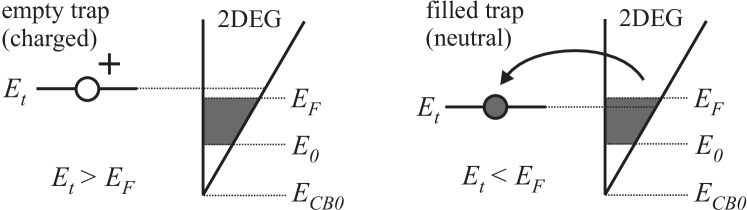
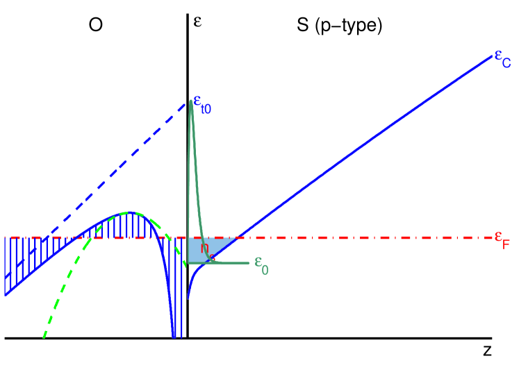
As described in the introduction, it is further assumed that a1) all trap states exist at the same energy if no external field is applied and posses a2) a spatially homogeneous density distribution in the oxide layer. But a potential gradient due to an applied gate voltage causes a linear increase of the trap energy position , where z is the distance from the Si/SiO2 interface () and is the distance between gate electrode and that interface (i.e. the thickness of the oxide layer).
For the electrostatic potential inside the oxide layer, also the screening effects of the inversion layer have to be taken into account. For 2D electrons in a Si-(001) layer, the screening radius is equal to . If the trap distance from the interface exceeds the screening radius, the in-plane components of the electrostatic field caused by the charged trap will effectively be screened. In that case, the electric field and the potential in the oxide can be described by the trap charge and an apparent mirror charge with opposite sign on the other side of the interface (assumption a4). The potential of the charged state caused by the image charge is in SI units with Fm-1 and , the relative dielectric constant of the oxide. Thus the total energy of the charged trap state can be given as
| (1) |
The last term in Eq. 1 leads to a down bending of the energetic position towards the interface and causes a maximum in the total trap energy as shown in Fig. 2.
The trap charge together with it’s mirror charge form a dipole perpendicular to the interface plane. Thus, for distances larger than , the scattering potential experienced by the 2D electrons can be described by a dipole field which falls of with (assumption a5). This is in agreement with the long range field of a screened Coulomb potential in two dimensions and leads to a consistent description. AM have calculated the classical scattering cross section for momentum relaxation for such a dipole field for electrons with kinetic energy as
| (2) |
with , the effective dielectric constant for the 2D electron system (2DES).
Whether a trap state is charged or not, depends on it’s energetical position relative to the Fermi energy (assuming thermal equilibrium for the occupation). The occupation function corresponds to a modified Fermi-Dirac distribution, where the degeneracy of empty and filled states is taken into account. AM have assumed that the (positively) charged trap state can have either spin up or down and is thus doubly degenerate, while the neutral state has no degree of freedom and is not degenerate. From that the probability of a trap state to be charged follows as
| (3) |
with the Boltzmann constant.
For the occupation of the trap states only the relative position of the trap energy to the Fermi energy is important. But the difference can not be derived directly – it has to be calculated from the two individual energies which depend on different variables. According to Eq. 1, the -dependence of the trap energy can be calculated, but one has to fix it’s zero-position . AM have assumed (a7) a fixed energetical distance of the trap state relative to the quantization energy of the electronic ground state in the (nearly triangular) inversion potential. But depends on the strength and shape of the inversion potential and via electron-electron interaction on the 2D electron density . Thus it seems not realistic that the energy of the trap state is fixed relative to , but rather that it is fixed relative to the energetic position of the conduction band edge (which is our improvement i2).
Equation 1 can be used as given, by noting that the energy is defined relative to the conduction band edge . On the other hand the ground state energy has to be calculated for the inversion potential, which itself depends on and the depletion charge and by including the electron-electron interaction AFS82 . As follows from the electron density AMnote , together with one gets the position of relative to the conduction band edge and the difference can be used for in Eq. 3.
In the Drude-Boltzmann approximation, the electrical resistivity , equal to the inverse conductivity
| (4) |
follows by calculating the effective transport scattering time . The detailed calculation is performed in Appendix A.
As a result one gets that
| (5) |
can be expressed by the effective values for the number of charged trap states per area, the electron velocity, the scattering cross section, and the average electron energy as given in Appendix A. These effective values depend on all the important variables of the systems, i.e. on , and so on. By inserting Eq. 5 into Eq. 4, one gets already the dependence of the resistivity on the different parameters
| (6) |
and we have verified equation Eq. 7 in Ref. Altsh99PRL, .
From here our treatment of the subject is quite different from that of AM Altsh99PRL . They have evaluated Eq. 6 analytically whereas we perform the calculation of it numerically. But in order to be able to solve Eq. 6, AM have used a parabolic (saddle-point) approximation for the -dependence of the trap energy (assumption a6). The analytical expression of AM (Eq. 9) contains a temperature independent prefactor and a temperature dependent scaling function . For their case (A) of the temperature dependence of , they get a critical behavior with increasing for and decreasing for (see Fig. 1 in Ref. Altsh99PRL, ), similar to what is observed experimentally. For their case (B), is always increasing with temperature and no critical behavior comes out.
In our numerical evaluation of Eq. 12, we use the exact dependence of as given by Eq. 1 (our improvement i1). The numerical treatment prevents errors due to the parabolic approximation, but enables us also to include further details, which also cannot be solved analytically.
AM have calculated the temperature dependence of the resistivity in close vicinity of the critical density where the behavior changes from metallic to insulating behavior. We have calculated also the direct density dependence over a larger range for different temperatures. Fig. 3 shows how the effective number of charge trap states depends on .
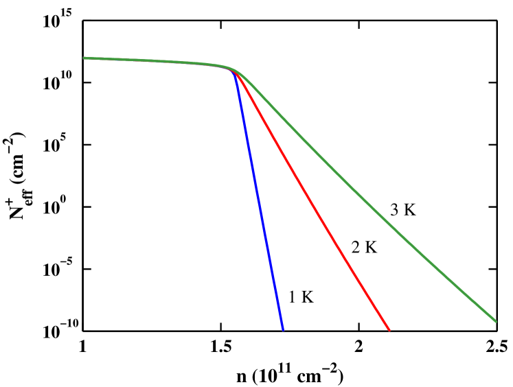
As can be seen there is a very strong variation above cm-2, where the maximum of the trap energy is just degenerate with . This strong variation comes from the fact that as soon as the maximum of is below only an exponentially small number of traps is still excited (i.e. charged) and the scattering efficiency decreases accordingly. As is nearly proportional to , such strong variations have not been observed experimentally. This discrepancy to the experiment can possibly be explained that in real 2D Si-MOS structures either the trap states do not have a -like distribution in energy or that in addition other scattering sources exist.
III Conclusions
We have shown that the numerical calculations of the temperature dependent resistivity give similar results as the analytical methods by AM. The strong density dependence of and thus of which follows from the calculation is not in agreement with experimental findings. In order to possibly resolve this discrepancy further calculations should be performed within the dipole trap model. The numerical procedure allows incorporation of further effects and realistic assumption like energetical broadening of the trap level, special spatial distributions of the defects, and detailed screening dependence.
Acknowledgements.
The authors would like to thank A. Prinz for his considerations on the dipole trap model and B. L. Altshuler and D. L. Maslov for helpful discussions. The work was supported by the Austrian Science Fund (FWF) with project P16160 on the “Metallic State in 2D Semiconductor Structures”.Appendix A Transport equations
The effective transport scattering time in the Drude-Boltzmann approximation follows from AFS82 ; noteTauWeighting
| (7) |
with being the energy dependent scattering time and the first derivative of the Fermi-Dirac distribution function .
The transport scattering time has to be calculated by integration over the individual scattering rates
| (8) |
with the density of charged traps , the spatially constant density of existing trap states (both being three dimensional volume densities) and the electron velocity.
By inserting the all expressions into Eq. 8 one gets
| (9) |
with the prefactor , an effective number of positive trap states per area , the effective width of positive charge layer and the position of the energetical maximum of the trap energy.
Further an effective energy can be defined so that formally Eq. 9 can be preserved for the effective , i.e. . A simple calculation gives
| (11) |
By further replacing the first derivative of the Fermi-Dirac function by the identity one obtains the same expression as Eq. 8 in Ref. Altsh99PRL, .
With these relations, the resistivity can exactly be written in terms of the effective energy as
| (12) |
which corresponds to Eq. 7 in Ref. Altsh99PRL, , but the individual terms are rewritten according to our definitions above. A comparison with Eq. 4 gives exactly
| (13) |
and shows that Eq. 8 can also be rewritten for effective values.
References
- (1) S. V. Kravchenko, et al. Phys. Rev. B 50, 8039 (1994); Phys. Rev. B 51, 7038 (1995).
- (2) for a review see e.g. S. V. Kravchenko and M. P. Sarachik, Rep. Prog. Phys. 67, 1 (2004).
- (3) E. Abrahams, P. W. Anderson, D. C. Licciardello, and T. V. Ramakrishnan, Phys. Rev. Lett. 42, 673 (1979).
- (4) F. Stern, Phys. Rev. Lett. 44, 1469 (1980).
- (5) A. Gold and V. T. Dolgopolov, Phys. Rev. B 33, 1076 (1986).
- (6) S. Das Sarma, Phys. Rev. B 33, 5401 (1986).
- (7) A. M. Finkelstein, Z. Phys. B: Condens. Matter 56, 189 (1984).
- (8) C. Castellani, C. Di Castro, P. A. Lee, and M. Ma, Phys. Rev. B 30, 527 (1984).
- (9) A. Punnoose and A. M. Finkelstein, Phys. Rev. Lett. 88, 016802 (2002).
- (10) G. Zala, B. N. Narozhny, and I. L. Aleiner, Phys. Rev. B 64, 214204 (2001).
- (11) I. V. Gornyi and A. D. Mirlin, Phys. Rev. B 69, 045313 (2004).
- (12) B. L. Altshuler and D. L. Maslov, Phys. Rev. Lett. 82, 145 (1999).
- (13) “Physics of Semiconductor Devices”, S. M. Sze, John Wiley & Sons, New York 1981, p. 379.
- (14) T. Ando, A. B. Fowler, and F. Stern, Rev. Mod. Phys. 54, 437 (1982).
- (15) “Gate Dielectrics and MOS ULSIs”, T. Hori, Springer Verlag, Berlin, 1997.
- (16) Note: In this work we use a temperature dependent Fermie energy instead of the chemical potential in contrast to AM, who used the nomenclature of beeing identical to the chemical potential at and using the chemical potential for any higher temperature.
- (17) Note: The type of trap states considered by AM might correspond to Si–Si weak bonds, which act like donors, i.e. being either neutral or positively charged. If the energetic position is deep inside the energy gap, it can also be seen as a hole trap state.
- (18) Note: In this work we calculate the Ferme energy inside the 2D layer according to the electron density . AM have considered two different cases in their work, the one discussed before is their case (B), whereas their case (A) assumes that the Fermi energy (chemical potential) of the 2DES and the Si substrate coincide and show the same temperature dependence. We do not consider case (A) in detail, as we think that case (B) is more realistic.
- (19) Note: The weighting of with the kinetic electron energy in Eq. 7 fundamentally follows from the Drude-Boltzmann approximation Smith as the Fermi velocity and the shift of the Fermi surface in k-space are both proportional to , which enter into the expression for the current . The integral in the denominator of Eq. 7 in 2D is just equal to the Fermi energy — also for elevated temperatures.
- (20) “Semiconductors”, R. A. Smith, Cambridge University Press, Cambridge 1964.