Fabrication and characterization of superconducting circuit QED devices for quantum computation
Abstract
We present fabrication and characterization procedures of devices for circuit quantum electrodynamics (cQED). We have made cavities with quality factors in the range , which allow access to the strong coupling regime of cQED. The cavities are transmission line resonators made by photolithography. They are coupled to the input and output ports via gap capacitors. An Al-based Cooper pair box is made by e-beam lithography and Dolan bridge double-angle evaporation in superconducting resonators with high quality factor. An important issue is to characterize the quality factor of the resonators. We present an RF-characterization of superconducting resonators as a function of temperature and magnetic field. We have realized different versions of the system with different box-cavity couplings by using different dielectrics and by changing the box geometry. Moreover, the cQED approach can be used as a diagnostic tool of qubit internal losses.
Index Terms:
Distributed parameter circuits, Q factor, Scattering parameters measurement, Superconducting cavity resonators.I Introduction
We have recently demonstrated that a superconducting quantum two-level system can be strongly coupled to a single microwave photon [1]. The strong coupling between a quantum solid state circuit and an individual photon, analogous to atomic cavity quantum electrodynamics (CQED) [2], has previously been envisaged by many authors, see [3] and references therein. Our circuit quantum electrodynamics architecture [3], in which a superconducting charge qubit, the Cooper pair box (CPB) [4], is coupled strongly to a coplanar transmission line resonator, has great prospects both for performing quantum optics experiments [5] in solids and for realizing elements for quantum information processing [6] with superconducting circuits [7] and also for other architectures [8].
In developing these qubit-resonator systems, one key ingredient is to design and realize transmission line resonators with high internal quality factor, , and with resonant frequency, , in the range to match the other energy scales of our device, and to be in the quantum regime () at . On the other hand, the resonator is loaded with input and output capacitances and we need a loaded quality factor in order to obtain reasonably fast rate of measurement, .
In fabricating the transmission line resonator, we opted for a coplanar waveguide (CPW) for many different reasons. First, a CPW has a simple layer structure with no need for deposited insulators. Second, it has a balanced structure with a relatively easy planar connection to the CPB. Third, a CPW has a that is relatively insensitive to kinetic inductance and dominated by geometrical distributed inductance. Last but not the least, CPW-based structures, made by Al thin film deposited on sapphire, have been recently shown [9] to allow very high (order of ).
We decided to fabricate on passivated Si wafers because this is the substrate on which we had previously developed the qubit fabrication. We also decided to try as material for the resonators both Al, for easy compatibility with the qubit process, and Nb, because its higher critical temperature allows testing of resonators at higher temperatures.
In section II, we present design consideration for devices for circuit quantum electrodynamics (cQED). We will show that we can engineer with different coupling of the resonator to the input and output ports and that the internal losses can be made negligible at the designed [1]. Section III introduces the fabrication procedures for both the resonator and the CPB. Section IV-VI present an RF-characterization of the superconducting transmission line resonators versus temperature and magnetic field.
II Circuit design
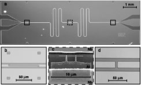
A picture of a chip containing a superconducting Nb CPW resonator is shown in Fig. 1a. The length of the meandering resonator is . The center conductor is wide, separated from the lateral ground planes extending to the edges of the chip by a gap, resulting in a wave impedance of the coplanar waveguide of to match the impedance of conventional microwave components. The capacitance per unit length is which gives a total resonator capacitance of . The resonator is coupled by identical capacitors at each end (see solid line square in Fig.1a) to an input and output feed line, fanning out to the edge of the chip and keeping the impedance constant. In Fig. 1b and 1d are shown micrographs of two of the coupling capacitors with different geometries. The one in Fig. 1b consists of two long and wide fingers separated by a gap. It has a capacitance, , larger than that in Fig.1d, which has a simpler geometry with a gap and .
The capacitive coupling to the input and output lines, together with the loading impedance, , are very important in determining the loaded quality factor , defined by the following equations:
| (1) |
where the external quality factor is
| (2) |
with
| (3) |
There are two possible regimes for the resonator. It can be undercoupled when is small (like ) and then . This is the regime in which it is possible to measure . Otherwise, the resonator can be overcoupled when is large (like ) and then . It is then possible to engineer the to obtain fast measurement with much larger than the qubit decay rates [1].
In Fig. 1c an electron micrograph of a Cooper pair box is shown. The CPB consists of a long and wide superconducting island parallel to the center conductor which is coupled via two size Josephson tunnel junctions to a much larger superconducting reservoir. The CPB is fabricated onto the silicon substrate (see dashed line square in Fig.1a) in the gap between the center conductor (top) and the ground plane (bottom) at an antinode of the electric field in the resonator. The Josephson junctions are formed at the overlap between the island and the fingers extending from the reservoir, which is capacitively coupled to the ground plane. The CPB is a two-state system described by the hamiltonian where is the electrostatic energy and is the Josephson energy. The overall energy scales of these terms, the charging energy and the Josephson energy , can be readily engineered during the fabrication by the choice of the total box capacitance and resistance respectively, and then further tuned in situ by electrical means. A flux bias , applied with an external coil to the loop of the box, controls . We have demonstrated that changing the length of the CPB island and its distance to the center conductor and changing the dielectrics (removing the passivation step of the Si substrate), we can obtain stronger couplings of qubit and resonator as predicted by simple electrostatic calculations of the capacitances.
III Device fabrication
The pattern of 36 different Nb resonators is generated exposing a bilayer photoresist ( LOR5A and S1813) through a mask with traditional UV photolithography. Then a thick Nb film is dc magnetron sputtered in Ar at with a rate of in an UHV system with a base pressure of . The substrate is a thick p-doped (Boron) oriented Si wafer with resistivity previously passivated by thermal wet oxidation with a thick layer of . A lift-off process in NMP followed by ultrasonic agitation completes the resonator fabrication.
Al resonators are fabricated on the same type of substrate depositing a thick Al film by thermal evaporation at a rate of in the same UHV system. Then the same mask is used to expose a single photoresist layer ( S1813) and then realized by wet etching () the metal.
In both cases, chips containing individual resonators are obtained by dicing the Si wafer. The CPB qubit (Fig. 1c) is then fabricated on an individual resonator by a simple Dolan bridge technique [10] exposing a bilayer resist ( MMA-(8.5)MAA EL13 and 950K PMMA A3) by e-beam lithography and then e-beam evaporating Al ( for the base and for the top electrode) at a rate of in a double-angle UHV system with a base pressure of . The junction barrier is realized with a thermal oxidation in a of . A lift-off process in hot acetone and ultrasonic agitation complete the device. To couple the qubit reservoir to ground with a large capacitance, the base electrode is deposited with a little angle taking advantage of the shadow of the thicker Nb film to define the capacitor.
IV Measurement technique
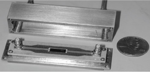
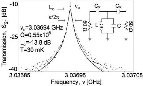
The frequency dependence of the transmission through the resonators [11] was measured using a vector network analyzer. The equivalent circuit of the measurement setup is shown in the inset of Fig. 3. The sample was mounted on a PC board in a closed copper sample box (Fig. 2) equipped with blind mate SMP connectors that launch the microwaves onto the PC board CPW’s. The sample was cooled to temperatures ranging from the critical temperature, of the superconducting films down to .
The transmission through the resonator around its fundamental resonant frequency is shown in Fig. 3 at . The curve was acquired using a input power [12] and a room temperature amplifier. The input power was lowered until no distortion of the resonance curve due to excessive input power could be observed. The network analyzer was response calibrated () up to the input and output ports of the cryostat and the absorption of the cabling in the cryostat was determined to be approximately in a calibrated and reflection measurement. The quality factor of the resonator is determined by fitting a Lorentzian line to the measured power spectrum as shown by the solid line in Fig. 3. This is the power spectrum of an undercoupled resonator and from the fit we have extracted . At this frequency the insertion loss is . The quality factor is determined from the full width at half max of the fitted power spectrum and is found to be .
V Temperature dependence of and
In Fig. 4, we show the measured temperature dependence of the quality factor for an undercoupled resonator (solid dots) and an overcoupled one (open dots). The lines in Fig. 4 are generated by summing a that scales exponentially with the reduced temperature, , in parallel with a constant . At low temperature, the coupling saturates the of the overcoupled resonator, while it seems that for the undercoupled one has still some weak temperature dependence whose nature is still unknown. We speculate that either vortices or losses in the dielectrics could limit the of this resonator but neither of these interpretations offer an easy understanding of the weak temperature dependence.
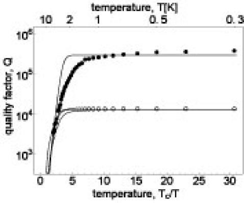
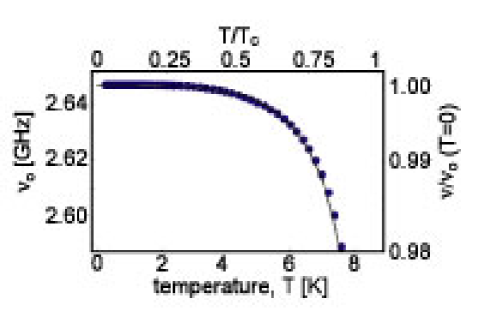
We have observed a shift of the resonant frequency with temperature as shown in Fig. 5, which can be understood in terms of the temperature dependent kinetic inductance of the resonator [9, 13]. is proportional to , where the total inductance of the resonator is the sum of the temperature independent geometric inductance and the temperature dependent kinetic inductance . The kinetic inductance scales as , where is the temperature dependent London penetration depth. The best fit in Fig. 4 was achieved for a ratio and a critical temperature of , which we have independently measured on a test sample fabricated on the same wafer.
VI Magnetic field dependence of
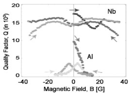
As explained in section II, we need to apply a magnetic field perpendicular to the qubit loop in order to tune . Then, we measured the quality factor of two resonators as a function of the magnetic field at , as shown in Fig. 6. It is evident that the Nb film (upper part) is less sensitive to the applied field than the Al film (lower part). In both cases there seems to be a reproducible and irreversible hysteretic behavior that can be reset by thermal cycling the sample. In our recent works [1], we have observed a focusing effect on the magnetic field such that the effective field in the gap of the resonator was approximately two orders of magnitude larger than the applied magnetic field. We believe that the hysteretic phenomena could be in fact a result of vortices being trapped in the resonator film due to these large effective fields.
VII Conclusion
In summary, we have designed and fabricated devices for realizing a circuit quantum electrodynamics architecture in which a qubit can be strongly coupled to a single microwave photon. We have shown that we can engineer with different coupling of the resonator to the input and output ports and that the internal losses can be made negligible at the designed . Indeed, we have achieved high in the undercoupled CPW resonators and in the overcoupled ones, which allow fast measurement of the qubit.
To help determine the mechanism of the losses, one can fabricate resonators on different substrates (Si with different resistivity, sapphire, )), or in different superconductors (Ta, Al). In fact, quality factor measurements in this type of resonant circuits serve as a sensitive probe of material losses in dielectrics and superconductors in the GHz frequency range at millikelvin temperatures. These presently unknown properties may in fact pose a serious limit for all superconducting qubits, though the large internal already observed are highly encouraging. Better knowledge of the material losses, and techniques to characterize them, may be crucial not only for future improvements of circuit QED devices, but also for designing and realizing robust, long-lived superconducting qubits.
References
- [1] A. Wallraff, D. Schuster, A. Blais, L. Frunzio, R.-S. Huang, J. Majer, S. Kumar, S. Girvin, and R. Schoelkopf, ”Strong coupling of a single photon to a superconducting qubit using circuit quantum electrodynamics,” Nature 431, 162-167 (2004), (also arXiv: cond-mat/0407325). D. Schuster, A. Wallraff, A. Blais, L. Frunzio, R.-S. Huang, J. Majer, S. M. Girvin, and R. J. Schoelkopf, ”AC-Stark shift and dephasing of a superconducting quibit strongly coupled to a cavity field,” Phys. Rev. Lett., to be published (2004)(also arXiv: cond-mat/0408367).
- [2] H. Mabuchi and A. Doherty, ”Cavity quantum electrodynamics: Coherence in context,” Science 298, 1372-1377 (2002).
- [3] A. Blais, R.-S. Huang, A. Wallraff, S. Girvin, and R. Schoelkopf, ”Cavity quantum electrodynamics for superconducting electrical circuits: an architecture for quantum computation,” Phys. Rev. A 69, 062320 (2004).
- [4] V. Bouchiat, D. Vion, P. Joyez, D. Esteve, and M. H. Devoret, ”Quantum coherence with a single Cooper pair,” Physica Scripta T76, 165-170 (1998).
- [5] D. Walls and G. Milburn, Quantum optics, Berlin, Spinger-Verlag, 1994.
- [6] M. A. Nielsen and I. L. Chuang, Quantum computation and quantum information, Cambridge University Press, 2000.
- [7] Y. Nakamura, Y. A. Pashkin, and J. S. Tsai, ”S. Coherent control of macroscopic quantum states in a single- Cooper-pair box,” Nature 398, 786-788 (1999). D. Vion, A. Aassime, A. Cottet, P. Joyez, H. Pothier, C. Urbina, D. Esteve, and M.H. Devoret, ”Manipulating the quantum state of an electrical circuit,” Science 296, 886-889 (2002). J. M. Martinis, S. Nam, J. Aumentado, and C. Urbina, ”Rabi oscillations in a large Josephson-junction qubit,” Phys. Rev. Lett. 89, 117901 (2002). Y. Yu, S. Han, X. Chu, S.-I. Chu, Y. Wang, ”Coherent temporal oscillations of macroscopic quantum states in a Josephson junction,” Science 296, 889-892 (2002). I. Chiorescu, Y. Nakmura, C. J. P. M. Harmans, and J. E. Mooij, ”Coherent quantum dynamics of a superconducting flux qubit,” Science 299, 1869-1871 (2003). T. Yamamoto, Y.A. Pashkin, O. Astafiev, Y. Nakamura, J.S. Tsai, ”Demonstration of conditional gate operation using superconducting charge qubits,” Nature 425, 941-944 (2003). I. Chiorescu, P. Bertet, K. Semba, Y. Nakmura, C. J. P. M. Harmans, and J. E. Mooij, ”Coherent dynamics of a flux qubit coupled to a harmonic oscillator,” Nature 431, 159-162 (2004).
- [8] A. S. S rensen, C. H., van derWal, L. Childress, and M. D. Lukin, ”Capacitive coupling of atomic systems to mesoscopic conductors,” Phys. Rev. Lett. 92, 063601 (2004). L. Tian, P. Rabl, R. Blatt, and P. Zoller, ”Interfacing quantum optical and solid state qubits,” unpublished (also arXiv: quant-ph/0310057).
- [9] P. K. Day, H. G. LeDuc, B. A. Mazin, A. Vayonakis, and J. Zmuidzinas, ”A broadband superconducting detector suitable for use in large arrays,” Nature 425, 817 821 (2003).
- [10] G. J. Dolan, ”Offset masks for lift-off processing,” Appl. Phys, Lett. 31, 337-339 (1977).
- [11] The transmission is measured in , where is the voltage measured at the input port of the analyzer and is the voltage applied at the output port of the analyzer.
- [12] The input power is in where .
- [13] K. Yoshida, K. Watanabe, T. Kisu, and K. Enpuku, ”Evaluation of magnetic penetration depth and surface resistance of superconducting thin films using coplanar waveguides,” IEEE Trans. on Appl. Supercond. 5, 1979-1982 (1995).