Bandstructure Effects in Multiwall Carbon Nanotubes
Abstract
We report conductance measurements on multiwall carbon nanotubes in a perpendicular magnetic field. A gate electrode with large capacitance is used to considerably vary the nanotube Fermi level. This enables us to search for signatures of the unique electronic band structure of the nanotubes in the regime of diffusive quantum transport. We find an unusual quenching of the magnetoconductance and the zero bias anomaly in the differential conductance at certain gate voltages, which can be linked to the onset of quasi-one-dimensional subbands.
Quantum transport in multiwall carbon nanotubes has been intensely studied in recent years DekkerReview ; Schoenenberger . Despite some indications of ballistic transport even at room temperature Frank ; Urbina , the majority of experiments revealed typical signatures of diffusive quantum transport in a magnetic field such as weak localization (WL), universal conductance fluctuations (UCF) and the -periodic Altshuler-Aronov-Spivak (AAS) oscillations Langer ; Schoenenberger ; LiuAvouris ; Bachtold_AB . These phenomena are caused by the Aharonov-Bohm phase, either by coherent backscattering of pairs of time-reversed diffusion paths (WL and AAS) or by interference of different paths (UCF). In addition, zero bias anomalies caused by electron-electron interactions in the differential conductance have been observed Bachtold_Tunnel . In those experiments, the multiwall tubes seemed to behave as ordinary metallic quantum wires. On the other hand, bandstructure calculations for singlewall nanotubes predict strictly one-dimensional transport channels, which give rise to van Hove singularities in the density of statesSaitoDresselhaus . Experimental evidence for this has been obtained mainly by electron tunneling spectroscopy on single wall nanotubes TansDekker393 . In this picture of strictly one-dimensional transport a quasiclassical trajectory cannot enclose magnetic flux and no low-field magnetoconductance is expected. Hence, the question arises how the specific band structure is reflected in the conductance as well as in its quantum corrections and how those on first glance contradictory approaches can be merged into a consistent picture of electronic transport.
In this experiment, we use a strongly coupled gate, which is efficient enough to shift the Fermi level through several quasi-onedimensional subbands. At certain gate voltages, which can be associated with the bottoms of the subbands, we observe a strong suppression of both the magnetoconductance and the differential conductance.
The samples were produced on top of thermally oxidized Silicon
wafers. First, Aluminium strips of 10 m width and 40 nm thickness
were evaporated. Exposure to air provides an insulating native oxide
layer of a few nm thickness. These strips serve as a backgate for the
individual nanotubes, which are deposited from a chloroform suspension
in the next step. Electric contacts are defined by electron beam
lithography. After application of an oxygen plasma, 80 nm of Gold are
deposited. In this way we achieve typical resistances between 10
k and 30 k at 4.2 K. The samples were
operated by a low frequency ac bias voltage and application of a dc
gate voltage to the Aluminium layer. Up to gate
voltages of 3 V no leakage current between the gate and the tube was
observed ( fA). Typical breakdown voltages of the
gate oxide were 3-4 V. Two-terminal resistance measurements were
carried out for two samples, A and B. The lengths of the samples are
5 m and 2 m and their diameters are 19
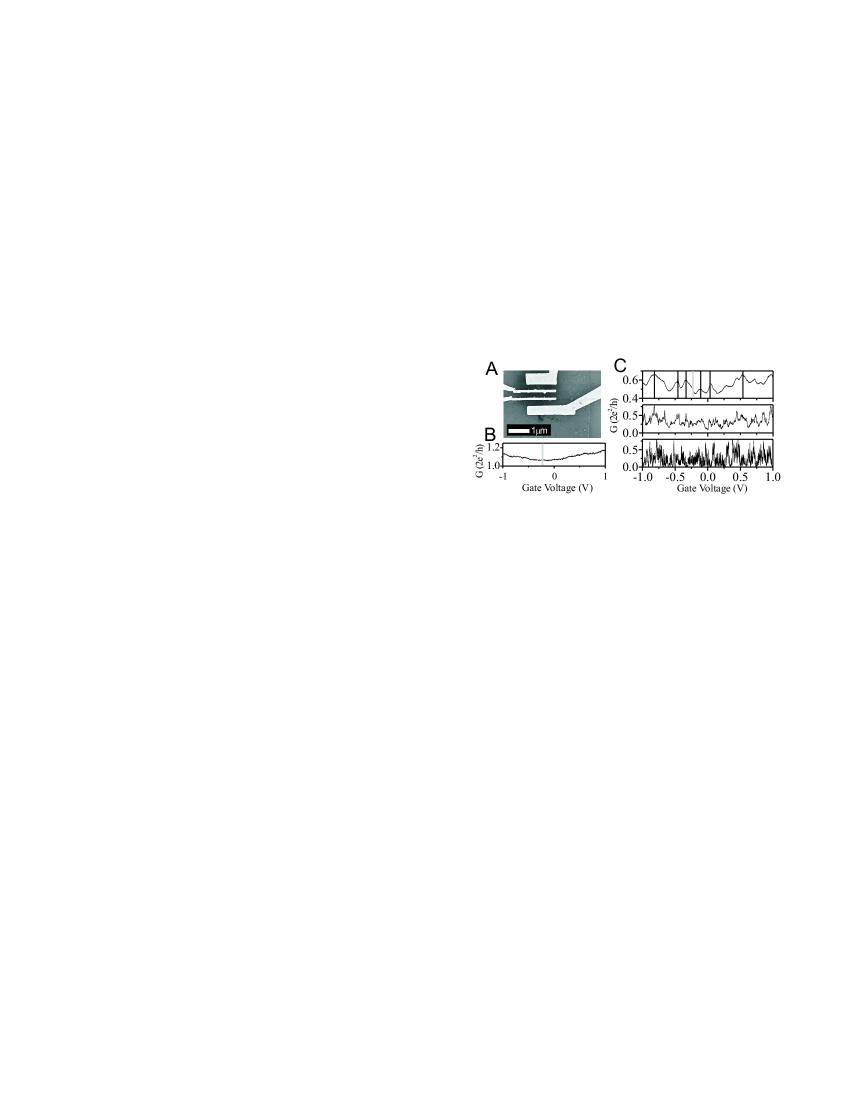
nm and 14 nm, respectively. A scanning electron micrograph
of a typical sample is presented in Fig. 1A.
In order to characterize the dependence of the conductance of sample A on , a small ac bias voltage of 2 V was applied and the current was measured at several temperatures (Fig. 1B,C). Fig. 1B shows the conductance as a function of gate voltage at 300 K. The corresponding curves for 10 K, 1 K and 30 mK are presented in Fig. 1C. The conductance at room temperature exhibits a shallow minimum located at 0.2 V. When the Fermi level is tuned away from the charge neutrality point, more and more subbands can contribute to the transport and an increase of the conductance is expected. Thus we attribute the position of the conductance minimum to the charge neutrality point, where bands with positive energy are unoccupied while those with negative energies are completely filled Krueger . This reveals the high efficiency of the gate as well as an intrinsic n-doping of the tube. The location of the minimum varied from sample to sample. We observed p- as well as n-doping at V in several samples. The curves in Fig. 1C show an increasing amplitude of the conductance fluctuations as the temperature is lowered, while the average conductance decreases. This can be interpreted as a gradual transition from a coexistence of band structure effects, UCFs and charging effects at 10 K and 1 K to the dominance of Coulomb blockade at 30 mK. In contrast to experiments on clean single wall nanotubes, no periodic Coulomb oscillations are found. Instead, irregular peaks in conductance occur. It is likely that disorder induces a nonuniform series of strongly coupled quantum dots and that transport is governed by higher order tunneling processes Bockrath .
Next, conductance traces were recorded at several
temperatures and in magnetic fields perpendicular to the tube
axis. The result at a temperature of 10 K is displayed as a color
plot in Fig. 2A.
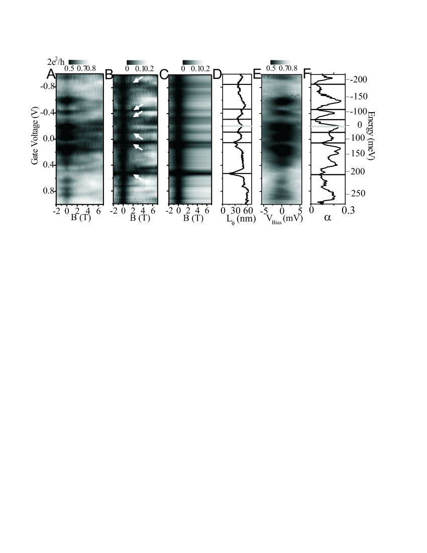
We have checked for several gate voltages that is symmetric
with respect to magnetic field reversal as required in a two point
configuration (not shown). In addition, most of the curves show a
conductance minimum at zero magnetic field. A closer look at the data
reveals that both the amplitude and the width of the conductance dip
vary strongly with gate voltage. In order to make this variation more
visible, we subtracted the curve at zero magnetic field (see Fig. 1C)
from all gate traces at finite fields. The deviation from the
zero-field conductance is presented as a color plot in Fig. 2B. The
most striking observation is that the magnetoconductance (MC)
disappears at certain gate voltages , as indicated by
arrows. These voltages are grouped symmetrically around the
conductance minimum at V in
Fig. 1B, which we have assigned to the charge neutrality point. The
position of the latter, as well as the gate voltages of MC quenches
have been indicated also in the linear response conductance curve
(Fig 1C) by red and black vertical lines, respectively. The latter
always coincide with conductance maxima. These observations lead us
to the conjecture that the quenched MC may occur at the onset of
subbands of the outermost nanotube shell, which is believed to carry
the major part of the current at low temperatures
Bachtold_AB .
To confirm this idea, we applied a simple bandstructure model. The
black line in Fig. 3A shows the density of states of a single wall
(140,140) armchair nanotube, which matches to the diameter of sample
A (19 nm).
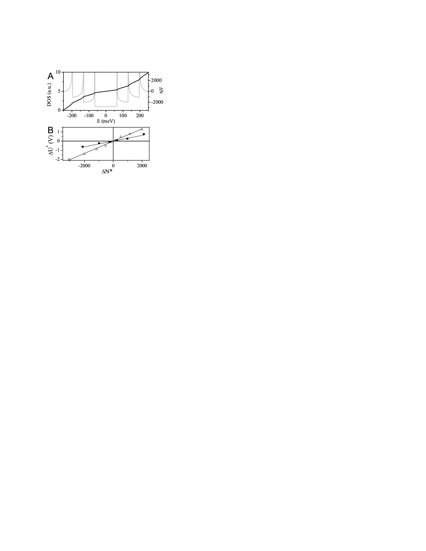
Typical van Hove singularities arise at the energies, where the
subband bottoms are located SaitoDresselhaus . By integration
over energy one obtains the number of excess electrons on
the tube, plotted as a red line in Fig. 3A. In this way, we can
determine the number of electrons at the onset of the
nanotube subbands. If we assume as usual a capacitative coupling
between the gate and the tube, can be converted into a
gate voltage via . In Fig. 3B the measured
gate voltages of quenched MC are plotted versus the calculated
for both samples. Both data sets fit very well into
straight lines, which demonstrates that most of the positions
of the quenched MC agree very well with the expected subband
onsets. In addition, the gate capacitances are provided by the
slope of vs. . The capacitances per length are
nearly identical, i.e. 120 aF/m and 129 aF/m for samples A
and B, respectively. These values agree within a factor of 2 with
simple geometrical estimates of , indicating the consistency of
the interpretation. From the capacitance and the calculated
dependence of the number of electrons on energy one can convert
the gate voltage into an equivalent Fermi energy. This energy scale
is shown in Fig. 2F.
The typical dip in the MC at in Fig. 2A has been observed
earlier and can be explained in terms of weak localization in absence
of spin-orbit scattering Schoenenberger ; LiuAvouris ; Tarkianinen . The weak localization correction
to conductance provides information on the phase coherence length
of the electrons. With being the measured diameter
and nm the electrode spacing of the nanotube, is given in the quasi-one-dimensional case () by , where is the magnetic length. In Fig. 2B each row displays a dip
around zero magnetic field, where both the amplitude and the width of
the dip vary strongly with gate voltage. We have used the weak
localization expression above to fit the low field MC with
and as free parameters. The conductance as calculated using the fit parameters is plotted in
Fig. 2C. We find that conductance traces are reproduced very well by
the fit for fields up to 2 T. For higher fields, deviations occur,
most probably due to residual universal conductance fluctuations. In
this way we obtain an energy dependent phase coherence length
, which is plotted in Fig. 2D.
varies from 20 to 60 nm and displays pronounced minima which
correspond to the regions of nearly flat MC in Fig. 2B. From the
preceding discussion, we can say that weak localization seems to be
suppressed at the onset of nanotube subbands.
In order to confirm the validity of our interpretation in terms of
weak localization, we have studied the temperature dependence of the
phase coherence length. As the dominating dephasing mechanism,
quasielastic electron-electron scattering has been identified
Schoenenberger ; LiuAvouris ; Stojetz . Dephasing by
electron-phonon scattering is negligible since the corresponding mean
free path exceeds 1 m even at 300 K
park ; javey . The theory by Altshuler, Aronov and Khmelnitzky
Altshuler_Aronov_Khmelnitzky predicts , where is the conductance, is the
diffusion constant, is the length of the tube. The dominance of
electron-electron-scattering can be confirmed by studying the
temperature dependence of . Therefore, the MC
measurements have been repeated for temperatures ranging from 1 K to
60 K. In order to eliminate the contribution of the universal
conductance fluctuations, the MC curves have been averaged over all
gate voltages. The result is plotted in Fig. 4A.
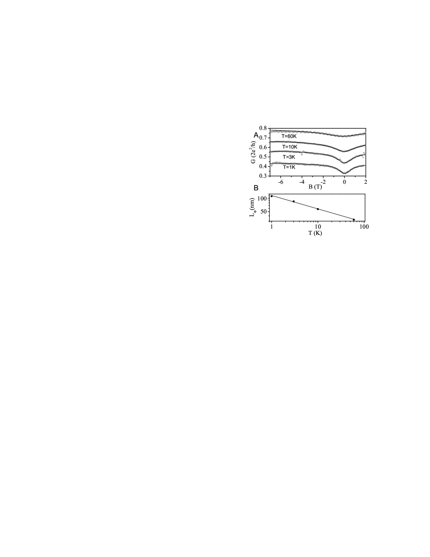
For the comparison of the curves with theory, one has to bear in mind
that the average runs also on curves with suppressed MC. Hence, for
the fit an averaged weak localization contribution of the form
with a scaling factor
has been taken into account. The fitted curves are included
in Fig. 4A. They match the data very well, up to magnetic fields of 7
T. In Fig. 4B the resulting are presented. The
contribution of the universal conductance fluctuations is completely
suppressed by ensemble averaging. The temperature dependence matches
a power law with exponent -0.31, which is close to the theoretical
prediction of -1/3.
Another quantum correction to the conductance is induced by the
electron-electron-interaction and reduces the density of states near
the Fermi energy EggerGogolin . This leads to zero bias
anomalies in the differential conductance d/d
Bachtold_Tunnel , from which information on the strength of the
electron-electron-interaction can be extracted. In the case of
tunneling into an interacting electron system with an ohmic
environment, the differential conductance d/d is given by a
power law, i.e. d/d for ,
where the exponent depends both on the interaction strength
and the sample geometry FisherKane . In order to obtain
complementary information, we have examined the dependence of the ZBA
on the gate voltage . The differential conductance has
been measured as a function of and . The
result is presented in Fig. 2E. For each gate voltage, the conductance
shows a dip at zero bias. The zero bias anomaly has a strongly varying
width with gate voltage and nearly vanishes at the same gate voltages
as the magnetoconductance. For each value of the
gate voltage, a power law fit for the bias voltage dependence of the
differential conductance has been performed. The resulting exponent
is plotted in Fig. 2F. varies between
0.03 and 0.3 and shows pronounced minima at the gate voltages .
We thus observe experimentally a strong correlation between the single
particle interference effects (expressed by ) and the
interaction effects (expressed by ). Both are strongly reduced
at certain positions of the Fermi level, which match well the
positions of the van Hove singularities estimated from simple
bandstructure models. What is the effect of the bandstructure?
Numerical calculations by Triozon et al. Triozon indicate that
the diffusion coefficient is not a constant as a function of
, but displays pronounced minima at the onset of new subbands. At
these points strong scattering occurs, resulting from the opening of a
highly efficient scattering channel. This has a direct effect on
. Of course,
may also be affected.
Can the energy dependence of also explain the
suppression of the interaction effects? This question has already been
raised by Kanda et al. Kanda , who also observed a pronounced
gate modulation of . For weak electron-electron-interaction
the theory of Ref. EggerGogolin predicts , where is the elastic mean free
path. This is definitely incompatible with the observed suppression of
at Fermi levels where diffusion is slow. The observed strong
modulations of and are accompanied by a rather
weak modulation of the zero bias conductance at 10 K (see
Fig. 1B). One may thus ask, whether the assumption of weak
interactions is valid. Taking the simple Drude formula as an orientation, this can be explained
by a partial compensation of the variation of and with . However, a quantitative explanation of the observed interplay
between bandstructure effects and quantum corrections to the
conductance requires a realistic model calculation for a thick, e.g.,
(140,140) nanotube including disorder and interaction effects. The
simple model of strictly one-dimensional conductance channels is
obviously incompatible with the observed weak-localization-like
magnetoconductance close to the charge neutrality point. The disorder
must be strong enough to mix the channels without completely smearing
the density of states.
In conclusion, our electronic transport measurements on multiwall
carbon nanotubes reveal an interplay of bandstructure effects
originating from the geometry of the tube and quantum interference
induced by disorder. The results demonstrate the necessity of a
systematic theoretical approach which can account both for disorder
and geometrical effects on the same level.
Acknowledgements.
We have benefitted from inspiring discussions with A. Bachtold, V. Bouchiat, G. Cuniberti, H. Grabert, M. Grifoni, K. Richter, S. Roche, R. Schäfer, C. Schönenberger and F. Triozon. Funding by the Deutsche Forschungsgemeinschaft within the Graduiertenkolleg 638 is acknowledged. The work in Lausanne was supported by the Swiss National Science Foundation.References
- (1) C. Dekker, Physics Today 52 22 (1999).
- (2) C. Schönenberger et al., Appl. Phys. A 69 283 (1999).
- (3) S. Frank et al., Science 280 1744 (1998).
- (4) A. Urbina et al., Phys. Rev. Lett. 90, 106603 (2003).
- (5) L. Langer et al., Phys. Rev. Lett. 76, 479 (1996).
- (6) K. Liu et al., Phys. Rev. B 63 161404 (2001).
- (7) A. Bachtold et al., Nature 397, 673 (1999).
- (8) A. Bachtold et al., Phys. Rev. Lett. 87, 166801 (2001).
- (9) R. Saito et al., J. Appl. Phys. 73 494 (1993).
- (10) S. J. Tans et al., Nature 393 49 (1998).
- (11) M. Krüger et al., New J. Phys 5 138.1 (2003).
- (12) P. L. McEuen et al., Phys. Rev. Lett. 83, 5098 (1999).
- (13) R. Tarkianinen et al., Phys. Rev. B 64, 195412 (2001).
- (14) B. Stojetz et al., New J. Phys 6 27 (2004).
- (15) J.-Y. Park et al., Nano Lett. 4, 517 (2004).
- (16) A. Javey et al., Phys. Rev. Lett. 92, 106804 (2004).
- (17) B. L. Altshuler, A. G. Aronov and D. Khmelnitzky, Solid State Comm. 39, 619 (1981).
- (18) R. Egger and A. O. Gogolin, Phys. Rev. Lett. 87, 066401 (2001).
- (19) C. L. Kane and M. P. W. Fisher, Phys. Rev. B 46, 15233 (1992).
- (20) F. Triozon et al., Phys. Rev. B 69, 121410 (2004).
- (21) A. Kanda et al., Phys. Rev. Lett. 92, 026801 (2004).