Spin characterization and control over the regime of radiation-induced zero-resistance states
Abstract
Over the regime of the radiation-induced zero-resistance states and associated oscillatory magnetoresistance, we propose a low magnetic field analog of quantum-Hall-limit techniques for the electrical detection of electron spin- and nuclear magnetic- resonance, dynamical nuclear polarization via electron spin resonance, and electrical characterization of the nuclear spin polarization via the Overhauser shift. In addition, beats observed in the radiation-induced oscillatory-magnetoresistance are developed into a method to measure and control the zero-field spin splitting due to the Bychkov-Rashba and bulk inversion asymmetry terms in the high mobility GaAs/AlGaAs system.
The interest in spintronics and spin-based semiconductor quantum computing has increased the regard for the spin degree of freedom, and especially semiconductor systems that allow for the control of spin.[1-12] Low Dimensional Electronic Systems[LDES] have consequently drawn special attention because, at low temperatures, , they include properties, which make possible relatively simple electrical detection- and radio-frequency () / microwave control- of nuclear- and electronic- spins. For example, microwave-induced Electron Spin Resonance (ESR) can be resistively detected in the quantum Hall regime, the ESR can be utilized to build up nuclear polarization via the flip-flop interaction, and the nuclear spin state can be subsequently characterized, also using an electrical measurement, by examining the back action of the nuclear magnetic field on the ESR.[13-19] Such electrical characterization techniques are valuable because they can potentially help to characterize the spin state over microscopic length scales.
Our studies have examined the above-mentioned approach towards the initialization, control, and readout of the nuclear spin polarization in spin domains within the LDES, with a view towards spintronic and quantum computing applications. The goals have been to develop the capability to measure and control a spin domain, to scale down its size to reduce the number of spins per domain, and to finally realize the capacity to simultaneously handle, i.e., measure and control, a multiplicity of domains on a single chip.[16-19]
Here, we propose the possibility of extending these quantum Hall spin measurement and control techniques into a low magnetic field limit, by building upon the recent observation of novel zero-resistance states,[20] which can be artificially induced and easily tuned by microwave excitation of the 2DES, at low magnetic fields, 0.5 T.[20-50] This new radiation-induced physical effect, which brings quantum-Hall-effect-like vanishing resistance states and activated transport characteristics to extremely low magnetic fields,[20,21] suggests possible future resistive spin detection and /microwave spin - manipulation techniques in the vicinity of zero magnetic field. An attractive feature of operating in the vicinity of zero-magnetic-field is that it is likely to increase the scope of possible future applications by simplifying device implementation.
Thus, we suggest the electrical detection of ESR in the domain of the microwave induced zero-resistance states, with the aim of utilizing the ESR to build up nuclear spin polarization in a weak magnetic field limit. A polarized nuclear spin system might subsequently be characterized at low through the detection of the Overhauser shift of the electrically detected ESR in the regime of the radiation induced zero-resistance states.[51] This approach might also be utilized to measure the spin relaxation and coherence times in the vicinity of null magnetic field.
Additionally, a lineshape study of beats in the radiation induced oscillatory magnetoresistance is applied to extract the electronic spin-splitting due to spin-orbit effects in the vicinity of zero-magnetic field.[27] A suggestion is also made for the measurement, manipulation, and control of the Zero-field Spin Splitting (ZFSS) using this technique.
The paper is organized as follows: Section II presents background and related work on electrical detection and the rf/microwave spin techniques in the quantum Hall regime. Section III(A) illustrates experimental results, which demonstrate the functionality of the approach described in section II. Section III(B) exhibits the relevant characteristics of the radiation-induced zero-resistance states observed in the low field limit. Section III(C) examines the suggested approach for characterizing the zero-field spin splitting in high mobility 2D electron systems using the radiation-induced resistance oscillations. Finally, section IV extends, by analogy, the quantum Hall spin detection techniques into the regime of the radiation-induced zero-resistance states, and sketches the control, using measurement feedback, of the zero-field spin splitting in the GaAs/AlGaAs system.
I Background
A two-dimensional electron system (2DES) at high magnetic fields exhibits Landau quantization, and disorder leads to level broadening, along with the localization of states between the Landau subbands, in the low limit.[13] When the Fermi level in the 2DES is pinned amongst the localized states, a quantized Hall effect is manifested by zero-resistance states, i.e., 0, and quantized plateaus in the Hall resistance, . Here, 0 is the asymptotic behavior in the limit. In practice, at liquid helium temperatures, a finite resistance is observed, and follows an activation law, i.e., , where is an activation energy.[13]
A non-vanishing electronic -factor removes the spin degeneracy. When the Fermi level is pinned in the localized states between spin split subbands, the system exhibits, once again, activated transport leading into zero-resistance states. Then, the conditions become favorable for the measurement and control, with spatial resolution, of nuclear and electronic spins in such systems. In particular, Electron Spin Resonance(ESR) induced, for example, by microwave excitation, becomes observable in the electrical response.[14,17-19,51] Further, under steady state ESR, the decay of spin-excited electrons leads to the spin polarization of nuclei via the flip-flop, electron-nuclear hyperfine interaction. The magnetic field arising from the spin polarized nuclei then provides a back action on the electrons, leading to an Overhauser shift in the electrically detected ESR, which can then serve to characterize the magnetic state of the nuclear spin system.
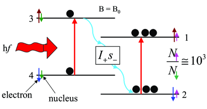
The hyperfine (spin-spin) interaction between an electron, , and a nucleus, , = ,[14,51] implies a four - level system for spin- particles (see Fig. 1). The saturation of the electron spin resonance by the application of intense microwave radiation tends to equalize the electronic population of the levels, while the phonon-assisted ’flip-flop’ exchange of spin between electrons and nuclei through the off-diagonal term provides a mechanism for realizing a steady state, see Fig. 1, which includes a large population difference between the nuclear spin states.[17-19,51] As the effective Boltzmann factor describing the steady state nuclear spin polarization comes to be determined by the electronic spin-flip energy (Fig. 1), it is, in principle, possible to realize a large nuclear spin polarization using this technique at a relatively high temperature.[51] A build up of the nuclear spin polarization by ESR also generates a nuclear magnetic field, , via the nuclear magnetic moment, which modifies the spin resonance condition for electrons. Thus, there is a characteristic B-field shift of the ESR with the spin polarization of nuclei, as mentioned previously, that is proportional to the nuclear magnetic field, . This Overhauser shift makes it possible to characterize the nuclear spin state through a measurement of the electrically detected ESR. In addition, dynamic nuclear polarization implies that the electrical resistance becomes sensitive to the nuclear spin state, suggesting also the possibility of nuclear magnetic resonance detection through a resistance measurement.[14-19]
Thus, such physical phenomena can, in principle, be utilized to realize discrete, independently controlled, and separately measured nuclear spin domains. In particular, nuclear spin initialization to a logic state can be achieved at a relatively high temperature by applying dynamic nuclear polarization. A local operation on a single domain can be implemented by introducing or removing electrons into the nuclear neighborhood using a voltage controlled ’gate,’ as the specimen is irradiated with a global microwave field. A state would then follow from a state upon spin-rotation with a radio-frequency -pulse. A superposition of and states might be realized by initializing a domain and then subjecting it to resonant radio frequency pulse. Readout of the nuclear spin state is accomplished by detecting the shift in the electrically detected ESR due to the nuclear magnetic field. Here, the and states will exhibit opposite Overhauser shifts, while state superposition might be reflected as an oscillatory Overhauser shift.[16-19] According to the theoretical studies of Taylor and co-workers,[52] an ensemble of nuclei, i.e., a nuclear spin domain, can serve as a repository or storage media for the quantum information associated with a mobile electronic qubit, and it is possible, in principle, to transfer quantum information in both directions, between the mobile electronic qubit and the nuclear spin domain with high fidelity. The operations described above can serve, for example, to prepare the spin domains for such a function.
II Experiment
II.1 Spin measurement and control in the quantum Hall regime
In this section, some concepts associated with the above-mentioned approach are illustrated through experiment. For this purpose, measurements were carried out on GaAs/AlGaAs specimens, which were mounted inside a waveguide, in a low temperature cryostat including a superconducting magnet. The samples were typically irradiated with amplitude-modulated microwaves over the frequency range GHz, as a double lock-in technique was employed to extract the microwave induced signal, , that exhibits ESR. For NMR measurements, the specimens were subjected to simultaneous microwave and rf excitation, with the rf spanning the range MHz. [16-19]
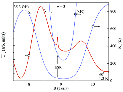
Figure 2 shows the typical transport response of a 2DES device under microwave excitation at 35.3 GHz. In this swept-, fixed- experiment, the microwave excitation helps to realize a resonance condition, when the photon energy, , matches the level spacing of the electron spin-split bands, and this leads to a resonant heating of the electron system, which is manifested as a detectable change in the electrical resistance. As illustrated in Fig. 2, the microwave induced signal , exhibits such ESR in the vicinity of 9 Tesla.
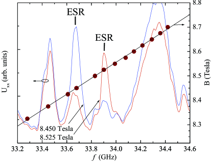
Figure 3 exhibits electrically detected ESR in a complementary fixed-, swept- experiment. The fixed- experimental data shown in Fig. 3 indicate non-monotonic, -insensitive, microwave-induced signals , which are attributed to -dependent radiation intensities at the sample. In addition, there is a strong -sensitive response vs , which is the ESR signal. In order to characterize the resonance, the lineshape of the ESR signal was fit with Gaussian and Lorentzian lineshapes. Such fits indicated an inhomogeneous broadening contribution to for electrons.
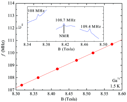
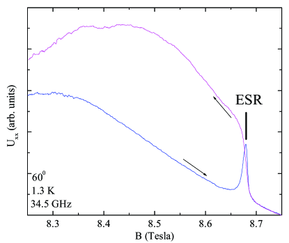
A role for dynamic nuclear polarization in such experiments can be motivated by exhibiting hysteretic transport in, for example, fixed-, swept- measurements, of the type shown in Fig. 4. Here, in Fig. 4, a broad linewidth observed in the down-sweep measurement is a manifestation of the Overhauser shift since a nuclear magnetic field compensates for the reduced applied magnetic field, and helps to maintain the ESR condition even below the where ESR would normally occur.
The role for nuclear polarization in this line broadening can be confirmed by examining the sensitivity of the electrical resistance to nuclear magnetic resonance (NMR). For this purpose, microwave and rf excitation were simultaneously applied to the specimen, with the rf chosen to coincide with the nuclear magnetic resonance frequency of the host nuclei, i.e., Ga or As. The observation of electrically detected NMR, illustrated in Fig. 5, confirm that enhanced nuclear polarization is responsible for the hysteretic transport observed in Fig. 4.
II.2 Novel radiation-induced zero-resistance states
The spin manipulation and measurement techniques described in the previous section operate in a quantum Hall regime characterized by activated transport and vanishing resistance, typically at high magnetic fields. Yet, the high field requirement is likely to complicate real-world applications. The question then arises whether there is a possibility of realizing and implementing a similar approach in a low- limit. Basically, from the perspective of the experimentalist, this seems to require bringing the essential quantum Hall features, vanishing resistance and activated transport, to the vicinity of zero magnetic field. We describe new phenomena below, which help to bring such quantum Hall features to the desired low magnetic field. The approach includes the added benefit of simple tunability of the zero-resistance states.
Briefly, experiments indicate that ultra high mobility GaAs/AlGaAs heterostructures including a 2DES can exhibit novel quantum-Hall-like vanishing resistance states, without Hall resistance quantization, at low temperatures, , and low magnetic fields, , when the specimen is subjected to Electro-Magnetic (EM) wave excitation. Zero-resistance-state occur about, for example, and , of the characteristic field , where is the electron mass, is electron charge, and is the EM-wave frequency, as the resistance-minima follow the series with … Temperature-dependent measurements on the observed resistance-minima also indicate activated transport.[20] Simply put, these novel zero-resistance states exhibit the desired quantum Hall characteristics so far as our objectives are concerned.
For the associated experiments, specimens were fabricated from ultra high mobility GaAs/AlGaAs heterostructures exhibiting a mobility up to . Typically, the sample was once again mounted inside a waveguide, immersed in pumped liquid Helium, and irradiated with microwaves, this time over the range GHz.[20]
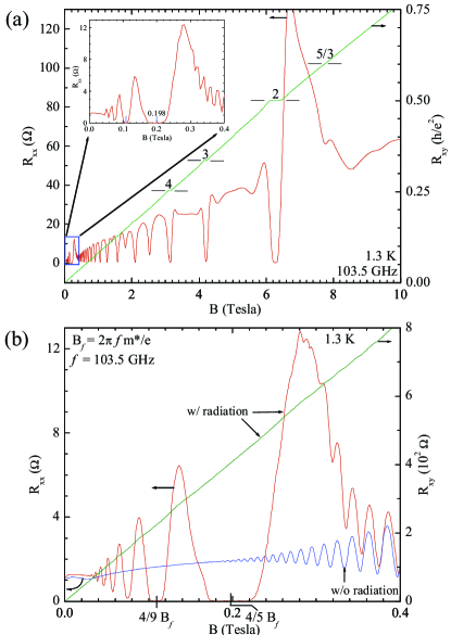
Fig. 6 (a) shows the diagonal ) and Hall () resistances measured in the four-terminal configuration. Here, and exhibit the usual quantum Hall behavior for 0.4 Tesla even under microwave excitation at = 103.5 GHz. In contrast, at 0.4 Tesla, see inset, Fig. 6(a), a radiation induced signal occurs and, remarkably, the resistance vanishes over a broad B-interval about = 0.198 Tesla.
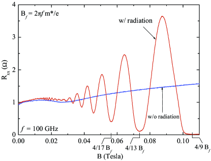
Further high-resolution measurements are shown in Fig. 6 (b). Without EM-excitation, exhibits Shubnikov-deHaas oscillations for 0.2 Tesla. The application of radiation induces additional oscillations, and, at the deepest minima, falls well below the resistance measured without radiation, as it vanishes around and . Although these resistance minima saturate at zero-resistance as in the quantum Hall regime, does not exhibit plateaus over the same -interval. We have found that minima occur = with …[20,48] As depends on , the periodicity of these radiation induced magnetoresistance oscillations changed with , and a given resistance minimum moved to higher B with increasing .
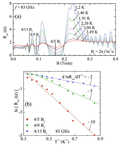
The temperature variation of at 85 GHz, shown in Fig. 7(a), displays both the strong -dependence of and the low- requirement for observation of the zero-resistance-states. The -variation of at the deepest minima demonstrate activated transport, i.e., , see Fig. 7(b), and the activation energy exceeds the Landau level spacing.[20,21]
These fundamental features, vanishing resistance and activated transport, are strongly reminiscent of the quantum Hall situation.[13] Indeed, since these two key features are the active ingredients, from the experimental perspective, for the functioning of the approach described in section II and III(A), there appears to be the possibility of utilizing these vanishing resistance states in lieu of the quantum Hall zero-resistance states, towards developing a low field analog of the approach suggested in section III(A).
It is true that there are measurable differences in the electrical transport between the regime of the radiation induced zero-resistance states and the regime of the quantum Hall effect, such as, e.g., the absence of Hall resistance quantization in the case of the microwave induced effect (Fig. 6(b)). Yet, since the Hall resistance is not actively used in the experimental measurements of spin resonance as in Figs. 2 - 5, we expect that Hall resistance quantization, or lack thereof, will not modify the functioning of the experimental technique. It appears that a key ingredient for the operation of the techniques of section III(A) is the suppression of the diagonal resistance, which originates from the residual scattering in the 2DES. Once this contribution has been suppressed, the resistance tends to reflect a special sensitivity, due to ”activated transport,” to the microwave induced ESR, and this is the physical feature that makes possible electrical detection of spin resonance.[14] From this perspective, it appears that the radiation induced zero-resistance states ought to serve as an adequate replacement for the quantum Hall resistance states.
II.3 Determination of the zero-field spin splitting from the radiation-induced oscillatory resistance
In the previous section,we demonstrated novel radiation induced zero-resistance states in the GaAs/AlGaAs system and reasoned that they could serve in lieu of quantum Hall zero-resistance states at low- in the development of electrical spin detection techniques for low magnetic field applications. Before further exploring such a possibility in the next section, we show here that beats observed in the low field radiation-induced resistance oscillations might serve as a sensitive probe of the zero-field spin splitting originating from the Bychkov-Rashba term and Bulk Inversion Asymmetry term in the high mobility 2DES.[53,54]
It is well known that mobile 2D electrons can experience, in their rest frame, an effective magnetic field that develops from a normal electric field at the semiconductor heterojunction interface due to the so-called Bychkov-Rashba effect.[53] As this magnetic field can, in principle, be controlled by an electrical gate, it has been utilized in the design of novel spin based devices such as the spin transistor.[2] In the 2DES realized in wider gap GaAs/AlGaAs, a Bulk Inversion Asymmetry (BIA) contribution to the ZFSS, can also provide a ”Zeeman magnetic field” as 0.[54-56] Although theory has suggested that the BIA term is stronger than the Rashba term in the GaAs/AlGaAs heterostructure 2DES,[57] ZFSS in -type GaAs/AlGaAs is not easily characterized because its signature is often difficult to detect using available methods.
Typical investigations of ZFSS in the 2DES look for beats in the Shubnikov-de Haas (SdH) oscillations that originate from dissimilar Fermi surfaces for spin-split bands.[58-60] Yet, it is known that other mechanisms can, in principle, provide similar experimental signatures.[59-61] Thus, a need has existed for new methods of investigating the spin-orbit interaction in the 2DES characterized by a small zero-field spin splitting, to supplement the Electron Spin Resonance, SdH, Raman scattering, and weak-localization based approaches.[14,59,62,63]
In this light, the approach outlined below is simpler and provides improved sensitivity because the ZFSS ( 20 eV) is determined through a comparison of the spin splitting with an easily tunable, small energy scale set by the photon energy ( 200 eV), unlike the SdH approach which relates the ZFSS ( 20 eV) to differences between two (spin split) Fermi surfaces with energy of order 10 meV in GaAs/AlGaAs.
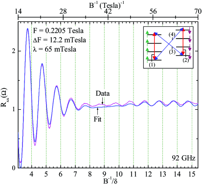
Fig. 8 illustrates the magnetoresistance observed with (w/) and without (w/o) microwave excitation, in a high mobility condition. The figure shows that, with radiation, there occur oscillations in as described in the previous section. Additionally, these oscillations show a non-monotonic variation in the amplitude, i.e., a beat, at low (see Fig. 8), as they extend to lower-. A study of the such transport data obtained at different revealed that, remarkably, the beat remains at a fixed with a change in the microwave frequency. Thus, a lineshape study was carried out in order to characterize this beating effect. Over a narrow -window above the beat, the oscillatory data could be fit with a single exponentially damped sinusoid: = , where is the amplitude, is the damping factor, and is the resistance oscillation frequency. Yet, a lineshape that included a superposition of two such waveforms proved unsatisfactory in modelling the data, when the data exhibited beats.
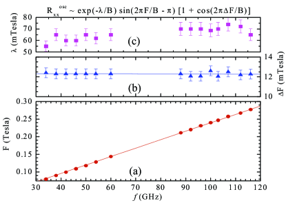
Thus, a candidate waveform , which can realize beats without phase reversal, was applied in the analysis. Representative data and fit, see Fig 9, show that this lineshape describes the data quite well. A summary of the fit parameters, , , and , is presented in Fig. 10. A noteworthy feature here is that the beat frequency, 12.3 mTesla, is independent of (see Fig. 10(b)).
This applied lineshape can be understood by invoking four distinct transitions between Landau subbands near the Fermi level, as in the inset of Fig. 9. Here, the spin-orbit interaction helps to remove the spin degeneracy of Landau levels as 0. If the oscillations originating from these terms have the same amplitude and share the same , then one expects a superposition of four terms: = , which constitutes the lineshape that has been utilized to fit the data.
Thus, beats observed in the radiation-induced resistance oscillations can be understood as a consequence of a zero-field spin splitting, due to the spin-orbit interaction.[2,53-60,62-66] One might relate to the ZFSS by identifying the radiation-frequency change, , that will produce a similar change in , i.e., = , where is the beat frequency, and is the rate of change of with the radiation frequency (see Fig. 10(a)). Then, the ZFSS corresponds to = 5.15 GHz or ( = 0) = = 21 eV. In comparison, theory suggests that, in the GaAs/AlGaAs heterostructure 2DES, the upper bound for the total ZFSS is 80 eV.[57]
A ESR study in the quantum Hall regime, as described in section III (A), showed that the ESR field, , varied as = 0.184 Tesla/GHz in the vicinity of filling factor = 1, which suggests that the effective Zeeman magnetic field is approximately = = 0.95 Tesla. Here, this is identified as the magnetic field that appears in the rest frame of the electron, in the absence of an applied magnetic field, due to the spin-orbit effects mentioned above.
III Extension of quantum Hall spin detection techniques to the regime of the radiation-induced zero-resistance states, and measurement and control of zero-field spin splitting
As reasoned above, electronic systems which exhibit vanishing resistance states and activated transport at high magnetic fields, include special features that make possible electrical detection of ESR and NMR. In section II, the essential physics behind this approach in the quantum Hall regime was reviewed. In section, III(A), experimental data were exhibited, which illustrated the viability of this approach in the quantum Hall regime. Although the concepts and techniques functioned as expected in the quantum Hall regime, the desirability of realizing a similar scheme in the low magnetic field limit was highlighted as part of the effort towards simplifying future device implementation. In section III(B), we demonstrated novel radiation induced zero-resistance states at low magnetic fields that included both the activated transport- and vanishing resistance states- characteristics of quantum Hall systems. In section III(C), we also suggested that beats in these novel radiation induced resistance oscillations might serve to directly measure the zero field spin splitting and the Zeeman magnetic field that appears in the rest frame of the electron due to the spin-orbit interaction.
Here, we outline, by analogy, an experimental scenario for electrical spin detection and dynamic nuclear polarization in the low limit, over the regime of the radiation-induced zero-resistance states: A high mobility 2DES might be irradiated with microwaves, at a frequency , in order to induce magnetoresistance oscillations, as in section III(B). For the appropriate radiation intensity, a zero-resistance state would be manifested in the vicinity of = (4/5) , where . Upon realizing the desired zero-resistance condition, a second radiation field at frequency is applied to the specimen in order to induce spin flip transitions or ESR in the vicinity of . The frequency of this radiation, , should be selected to match the total spin splitting. Due to the strong temperature sensitivity of the resistance at the radiation-induced zero-resistance states resulting from activation transport characteristics, see Fig 7 (b), ESR induced by the radiation field ought to be manifested as a change in the electrical resistance, just as in the quantum Hall situation (Fig. 2). One expects this behavior because, phenomenologically, the radiation at helps to suppress the residual scattering in the 2DES, and this should lead to an enhanced sensitivity to the ESR induced by , which might be viewed as a new resonant scattering channel.
A steady state ESR, perhaps in the presence of an oriented current, might then be applied to dynamically polarize nuclei via the flip-flop interaction. This could be manifested as a broadening of the ESR line in analogy to Fig. 4. One might now track the time evolution of the ESR line to measure the nuclear spin relaxation rate at low , and study its sensitivity to magnitude of the diagonal resistance of the specimen, which can be tuned with the radiation intensity at . Finally, one might apply an -field at a frequency in order to induce- and electrically detect- nuclear magnetic resonance, as in Fig. 5.
A goal would be to apply dynamic nuclear polarization and obtain polarized nuclear spin domains in the low magnetic field limit. Once polarized nuclear spin domains have been realized using the approach outlined above, -pulses might be applied to rotate the spin domain. Alternatively, one might examine the effect of magnetic field reversal with respect to the domain polarization axis, through such experiments.
The zero-field spin splitting measurement scheme of section III(C) might also be applied towards the characterization and control of the electronic spin splitting due to the Bychkov-Rashba and Dresselhaus terms in GaAs/AlGaAs.[53,54,64] According to Tarasenko and Averkiev,[64] beats should be observable when either the Bychkov-Rashba or the Dresselhaus terms are manifested in the specimen, and the beats should disappear when the two contributions are equal in magnitude. Thus, in a high mobility quantum well with a negligible electric field along the growth direction, one might first investigate the beats originating from the Dresselhaus effect. Then, a top-gate might be utilized to change the electric field along the growth direction and change/introduce the Bychkov-Rashba term.[64]
Perhaps, the top-gate can also be applied to change the electron spin resonance condition at a fixed magnetic field. Then, if one wishes to preferentially polarize the nuclear spin on one domain, while leaving the nuclear spin of other domains unchanged, the Bychkov-Rashba effect can be utilized to bring into- or take out of- the electron spin resonance condition the domain of interest, with the help of the top-gate, since the gate influence will be local only to the addressed domain.
IV Summary
The manipulation, measurement, and control of electronic and nuclear spin have been important themes in the spintronics paradigm,[1] which aims to realize novel devices that utilize also the spin degree of freedom.[65,66] Here, we have proposed spin measurement, manipulation, and control techniques, in a low magnetic field limit, in the high mobility GaAs/AlGaAs system. In particular, we have suggested the possibility of operating on nuclear spins via electrons and electrically detecting the results, at low magnetic fields, over the regime of the recently discovered radiation-induced zero-resistance states in the GaAs/AlGaAs system. As discussed, one might try to extend by analogy the experimentally demonstrated electrical-detection, rf/microwave manipulation techniques from the quantum Hall regime, into the low field limit, based on the observed phenomenological similarity of transport in the high field quantum Hall- and the low field radiation induced zero-resistance- regimes. Success in this direction might lead to discrete, independently controlled, and separately measured nuclear spin memory cells that function at low magnetic fields, and might potentially serve as a long-term repository for the quantum information associated with a mobile electronic qubit.[52]
We have also identified a possible new method for characterizing the ZFSS. In particular, observed beats in the radiation-induced magnetoresistance oscillations have been suggested as a tool for characterizing the zero-field spin splitting originating from the Bychkov-Rashba effect and BIA in the GaAs/AlGaAs system.[53,54] Characterization and control of the zero-field spin splitting in GaAs/AlGaAs might advance this widely available material, which provides the highest mobility 2DES, as a potential host for the realization of the spin based devices at low-.
Acknowledgements.
We acknowledge stimulating discussions with S. Saykin, M. Dobers, J. H. Smet, K. von Klitzing, V. Narayanamurti, W. B. Johnson, V. Privman, and D. Mozyrsky. High mobility material was kindly provided by V. Umansky.References
- (1) S. A. Wolf et al., ”Spintronics: A spin-based electronics vision for the future,” Science 294, 1488-1495 (2001).
- (2) S. Datta and B. Das, ”Electronic analog of the electro-optic modulator,” Appl. Phys. Lett. 56, 665-667 (1990).
- (3) D. P. DiVincenzo, ”Quantum Computation,” Science 270, 255 (1995).
- (4) C. H. Bennett, ”Quantum Information and Computation,” Physics Today 25-30 (Oct.1995).
- (5) L. K. Grover, ”The advantages of superposition”, Science 280, 5361 (1998).
- (6) B. E. Kane, ”A Silicon-based Nuclear Spin Quantum Computer,” Nature 393, 133 (1998).
- (7) D. Loss and D. P. DiVincenzo, ”Quantum Computation with Quantum Dots,” Phys. Rev. A 57, 120 (1998).
- (8) A. Imamoglu et al., ”Quantum Information Processing Using Quantum Dot Spins and Cavity-QED,” Phys. Rev. Lett. 83, 4204 (1999).
- (9) I. L. Chuang, N. Gershenfeld, and M. Kubinec, ”Experimental implementation of fast quantum searching,” Phys. Rev. Lett. 80, 3408 (1998).
- (10) V. Privman, I. D. Vagner, and G. Kventsel, ”Quantum Computation in Quantum-Hall Systems,” Phys. Lett. A 239, 141 (1998).
- (11) R. Vrijen et al., ”Electron-spin resonance transistors for quantum computing in silicon-germanium heterostructures,” Phys. Rev. A 62, 012306 (2000).
- (12) T. D. Ladd et al., ”All silicon quantum computer,” Phys. Rev. Lett. 89, 017901 (2002).
- (13) R. E. Prange and S. M. Girvin, (eds) The Quantum Hall Effect, 2nd Ed., New York: Springer-Verlag, 1990.
- (14) M. Dobers, K. von Klitzing, J. Schneider, G. Weimann, and K. Ploog, ”Electrical Detection of Nuclear Magnetic Resonance in GaAs/AlGaAs Heterostructures,” Phys. Rev. Lett. 61, 1650 (1988).
- (15) T. Machida et al., ”Spin polarization of fractional quantum Hall edge channels studied by dynamic nuclear polarization,” Phys. Rev. B65, 233304 (2002).
- (16) R. G. Mani, W. B. Johnson, V. Narayanamurti, V. Privman and Y. H. Zhang, ”Nuclear Spin Memory and Logic in Quantum Hall Semiconductor Nanostructures for Quantum Computing Applications,” Physica E 12, 152 (2002).
- (17) R. G. Mani, W. B. Johnson, and V. Narayanamurti, ”Manipulation and measurement of nuclear spin over the quantum Hall regime for quantum information processing,” Superlattices and Microstructures 32, 261 (2002).
- (18) R. G. Mani, W. B. Johnson, and V. Narayanamurti, ”Initialization of a nuclear spin system over the quantum Hall regime for quantum information processing,” in Proc. of 15th Intl. Conf. on the Appl. of High Magnetic Fields in Semicond. Physics, Oxford, Aug. 2002, IOP Conf. Ser. No. 171, eds. A. R. Long and J. H. Davies (IOP, Bristol, 2003) 1.6.
- (19) R. G. Mani, W. B. Johnson, and V. Narayanamurti, ”Nuclear spin based quantum information processing at high magnetic fields,” Nanotechnology 14, 515 (2003).
- (20) R. G. Mani, J. H. Smet, K. von Klitzing, V. Narayanamurti, W. B. Johnson, and V. Umansky, ”Zero-resistance states induced by electromagnetic-wave excitation in GaAs/AlGaAs heterostructures,” Nature (London) 420, 646 (2002).
- (21) M. A. Zudov, R. R. Du, L. N. Pfeiffer, and K. W. West, ”Evidence for a new dissipationless effect in 2D electronic transport,” Phys. Rev. Lett. 90, 046807 (2003).
- (22) R. Fitzgerald, ”Microwaves induce vanishing resistance in the two-dimensional electron system,” Phys. Today 56 (4), 24-27 (2003).
- (23) R. G. Mani, J. H. Smet, K. von Klitzing, V. Narayanamurti, and V. Umansky, ”Single particle and collective response in the magnetophotoresistance of a high mobility 2DES under microwave excitation,” Bull. Am. Phys. Soc. 46, p. 972 (2001).
- (24) M. A. Zudov, R. R. Du, J. A. Simmons, and J. L. Reno, ”Shubnikov-de Haas-like oscillations in millimeterwave photoconductivity in a high-mobility two-dimensional electron gas,” Phys. Rev. B 64, 201311 (2001).
- (25) P. D. Ye et al., ”Giant microwave photoresistance of two-dimensional electron gas,” Appl. Phys. Lett. 79, 2193 (2001).
- (26) R. G. Mani et al., ”Magnetoresistive response of a high mobility 2DES under electromagnetic wave excitation,” in the Proc. of the 26th Intl. Conf. on the Phys. of Semicond. Edinburgh, Aug. 2002, IOP Conf. Ser. No. 171, eds. A. R. Long and J. H. Davies (IOP, Bristol, 2003) H112; [cond-mat/0305507].
- (27) R. G. Mani et al., ”Radiation induced oscillatory magnetoresistance as a sensitive probe of the zero-field spin splitting in high mobility GaAs/AlGaAs devices,” Phys. Rev. B 69, 193304 (2004).
- (28) V. I. Ryzhii, Fiz. Tverd. Tela (Leningrad) 11, 2577 (1969) [Sov. Phys. - Sol. St. 11, 2078-2080 (1970)].
- (29) J. C. Phillips, ”Microscopic origin of collective exponentially small resistance states,” Sol. St. Comm. 127, 233 (2003).
- (30) A. C. Durst, S. Sachdev, N. Read, and S. M. Girvin, ”Radiation-induced magnetoresistance oscillations in a 2D electron gas,” Phys. Rev. Lett. 91, 086803 (2003).
- (31) A. V. Andreev, I. L. Aleiner, and A. J. Millis, ”Dynamical symmetry breaking as the origin of the zero-dc-resistance state in an ac-driven system,” Phys. Rev. Lett. 91, 056803 (2003).
- (32) P. W. Anderson and W. F. Brinkman, ”New zero-resistance state in heterojunctions: A dynamical effect,” cond-mat/0302129.
- (33) J. Shi and X. C. Xie, ”Radiation-induced zero-resistance state and the photon-assisted transport,” Phys. Rev. Lett. 91, 086801 (2003).
- (34) A. A. Koulakov and M. E. Raikh, ”Classical model for the negative dc conductivity of ac-driven two-dimensional electrons near the cyclotron resonance,” Phys. Rev. B 68, 115324 (2003).
- (35) F. S. Bergeret, B. Huckestein, and A. F. Volkov, ”Current-voltage characteristics and the zero-resistance state in a two-dimensional electron gas,” Phys. Rev. B 67, 241303 (2003).
- (36) I. A. Dmitriev, A. D. Mirlin, and D. G. Polyakov, ”Cyclotron-Resonance Harmonics in the ac Response of a 2D Electron Gas with Smooth Disorder,” Phys. Rev. Lett. 91, 226802 (2003).
- (37) S. I. Dorozhkin, ”Giant magnetoresistance oscillations caused by cyclotron resonance harmonics,” JETP Lett., 77, 577 (2003).
- (38) X. L. Lei and S. Y. Liu, ”Radiation-induced magnetoresistance oscillation in a two-dimensional electron gas in Faraday geometry,” Phys. Rev. Lett. 91, 226805 (2003).
- (39) V. Ryzhii and V. Vyurkov, ”Absolute negative conductivity in two-dimensional electron systems associated with acoustic scattering stimulated by microwave radiation,” Phys. Rev. B 68, 165406 (2003).
- (40) D. H. Lee and J. M. Leinaas, ”Role of interference in millimeter-wave-driven dc transport in a two-dimensional electron gas,” Phys. Rev. B 69, 115336 (2004).
- (41) V. Ryzhii, ”Microwave photoconductivity in two-dimensional electron systems due to photon-assisted interaction of electrons with leaky interface phonons,” Phys. Rev. B 68, 193402 (2003).
- (42) M. G. Vavilov and I. L. Aleiner, ”Magnetotransport in a two-dimensional electron gas at large filling factors,” Phys. Rev. B 69, 035303 (2004).
- (43) R. Klesse and F. Merz, ”Residual resistance in two-dimensional microwave driven systems,” preprint cond-mat/0305492.
- (44) A. F. Volkov and V. V. Pavlovskii, ”Residual resistance in a two-dimensional electron system: A phenomenological approach,” Phys. Rev. B 69, 125305 (2004).
- (45) V. Ryzhii and A. Satou, ”Electric-Field Breakdown of Absolute Negative Conductivity and Supersonic Streams in Two-Dimensional Electron Systems with Zero Resistance/Conductance States,” J. Phys. Soc. Jpn. 72, 2718 (2003).
- (46) R. G. Mani et al., ”Radiation induced zero-resistance states in GaAs/AlGaAs heterostructures: Voltage-current characteristics and intensity dependence at the resistance minima,” preprint cond-mat/0306388.
- (47) R. G. Mani, ”Zero-resistance states induced by electromagnetic-wave excitation in GaAs/AlGaAs heterostructures,” Physica E 22, 1 (2004) .
- (48) R. G. Mani et al., ”Demonstration of a 1/4-Cycle Phase Shift in the Radiation-Induced Oscillatory Magnetoresistance in GaAs/AlGaAs Devices,” Phys. Rev. Lett. 92, 146801 (2004).
- (49) R. G. Mani et al., ”Radiation-induced oscillatory Hall effect in high-mobility devices,” Phys. Rev. B 69, 161306 (2004).
- (50) S. A. Studenikin, M. Potemski, P.T. Coleridge, A. Sachrajda, and Z.R. Wasilewski ”Microwave radiation induced magneto-oscillations in the longitudinal and transverse resistance of a two dimensional electron gas”, Sol. St. Comm. 129, 341 (2004).
- (51) A. W. Overhauser, ”Polarization of nuclei in metals,” Phys. Rev. 92, 411 (1953)
- (52) J. M. Taylor, C. Marcus, and M. D. Lukin, ”Long-lived memory for mesoscopic quantum bits,” Phys. Rev. Lett. 90, 206803 (2003).
- (53) Y. A. Bychkov and E. I. Rashba, ”Oscillatory effects and magnetic suscepibility of carriers in inversion layers,” J. Phys. C. 17, 6039-6045 (1984).
- (54) G. Dresselhaus, ”Spin orbit coupling effects in zinc blende structures,” Phys. Rev. 100, 580 (1955).
- (55) G. Lommer, F. Malcher, and U. Rössler, ”Spin splitting in semiconductor heterostructures for B 0,” Phys. Rev. Lett. 60, 728-731 (1988).
- (56) R. Eppenga and M. F. H. Schuurmans, ”Effect of bulk inversion asymmetry on [001], [110], and [111] GaAs/AlAs quantum wells,” Phys. Rev. B. 37, 10923-10926 (1988).
- (57) E. A. De Andrada e Silva, G. C. La Rocca, and F. Bassani, ”Spin-split subbands and magneto-oscillation in III-V saymmetric heterostructures,” Phys. Rev. B 50, 8523-8533 (1994).
- (58) B. Das et al., ”Evidence for spin splitting in InGaAs/InAlAs heterostructures as B 0,” Phys. Rev. B 39, 1411 - 1414 (1989).
- (59) P. Ramvall, B. Kowalski, and P. Omling, ”Zero-magnetic fields spin splittings in AlGaAs/GaAs heterojunctions,” Phys. Rev. B 55, 7160-7164 (1997).
- (60) A. C. H. Rowe, J. Nehls, R. A. Stradling, and R. S. Ferguson, ”Origin of beat patterns in the quantum magnetoresistance of gated InAs/GaSb and InAs/AlSb quantum wells,” Phys. Rev. B 63, 201307 (2001).
- (61) T. H. Sander et al., ”Determination of the phase of magneto-intersubband scattering oscillations in heterojunctions and quantum wells,” Phys. Rev. B 58, 13856-13862 (1998).
- (62) B. Jusserand, D. Richards, G. Allan, C. Priester, and B. Etienne, ”Spin orientation at semiconductor heterointerfaces,” Phys. Rev. B 51, 4707-4710 (1995).
- (63) J. B. Miller et al., ”Gate-controlled spin-orbit quantum interference effects in lateral transport,” Phys. Rev. Lett. 90, 076807 (2003).
- (64) S. A. Tarasenko and N. S. Averkiev, ”Interference of spin splittings in magneto-oscillation phenomena in two-dimensional systems” JETP Letters, 75, 669-672, 2002.
- (65) S. Saykin, M. Shen, M. -C. Cheng, and V. Privman, ”Semiclassical Monte-Carlo mode for in-plane transport of spin-polarized electrons in III-V heterostructures,” J. Appl. Phys. 94, 1769-1776 (2003); S. Saykin, ”A Drift diffusion model for spin polarized transport in a non-degenerate 2DEG controlled by spin-orbit interaction,” J. Phys. Condens. Matter 16, 5071-5081 (2004).
- (66) Y. V. Pershin, J. A. Nesteroff, and V. Privman, ”Effect of spin-orbit interaction and in-plane magnetic field on the conductance of a quasi-one-dimensional system,” Phys. Rev. B 69, 121306 (2004); Y. V. Pershin, ”Drift diffusion approach to spin-polarized transport,” Physica E 23, 226-231 (2004).