Self-consistent study of electron confinement to metallic thin films on solid surfaces
Abstract
We present a method for density-functional modeling of metallic overlayers grown on metallic supports. It offers a tool to study nanostructures and combines the power of self-consistent pseudopotential calculations with the simplicity of a one-dimensional approach. The model is applied to Pb layers grown on the Cu(111) surface. More specifically, Pb is modeled as stabilized jellium and the Cu(111) substrate is represented by a one-dimensional pseudopotential that reproduces experimental positions of both the Cu Fermi level and the energy gap of the band structure projected along the (111) direction. The model is used to study the quantum well states in the Pb overlayer. Their analysis gives the strength of the electron confinement barriers at the interface and at the surface facing the vacuum. Our results and analysis support the interpretation of the quantum well state spectra measured by the scanning tunneling spectroscopy.
pacs:
73.21.Fg, 71.15.Mb, 68.35,-pI Introduction
The ability to manufacture desired nanostructures on solid surfaces by controlled growth or atomic manipulation techniques has increased enormously during the last decades. Ortega and Himpsel (1992); Chiang (2000) At the same time, spectroscopic methods to study different physical properties and phenomena of these structures have also experienced a huge development. In understanding and interpreting the ensuing experimental results rich of quantum phenomena, accurate theoretical and computational modeling plays a vital role.
A widely studied phenomenon is the growth of thin Pb films or extended Pb islands on solids, for example, on Si or Cu surfaces. The growth of Pb provides a laboratory to test the the so-called quantum size effects (QSE) arising due to the electron confinement perpendicular to the surface. The confinement results in discrete energy levels, the so-called quantum well states (QWS’s). With the increasing film thickness new QWS’s become occupied producing oscillations in the total energy, work function and other physical properties. The oscillations in the energy are the origin of the ”magic” islands heights. Otero et al. (2002); Hinch et al. (1989); Budde et al. (2000); Luh et al. (2001); Yeh et al. (2004); Hupalo and Tringides (2002); Mans et al. (2002); Hupalo et al. (2001); Su et al. (2001a); Menzel et al. (2003); Ogando et al. (2004a); Gavioli et al. (1999); Matsuda et al. (2004); Nagao et al. (2004)
The most important feature characterizing an overlayer or a nanoisland is its height. However, measurements based on different physical processes may provide different values. The x-ray diffraction Czoschke et al. (2003) can be used to directly determine the number of atomic monolayers (ML) in thin films. The scanning tunneling microscope (STM) Otero et al. (2002) gives the thickness of finite nanoislands. In the helium atom scattering (HAS) the specular returning point of He atoms is measured.Floreano et al. (2004); Hinch et al. (1989) STM and HAS reflect the electron density profile of the surface. Floreano et al. (2004); Hinch et al. (1989) The scanning tunneling spectroscopy (STS) measures the QWS spectrum and the width of the quantum well confining the electrons is evaluated from it. Otero et al. (2000) In addition to the overlayer-vacuum surface profile, the QWS spectrum is sensitive also to properties of the substrate-overlayer interface. The information about the confining quantum well is important not only for the determination of the the film thickness but also for the understanding and controlling the so-called ”electronic growth mode”.
In this work we model thin Pb films growing in the [111] direction on the Cu(111) surface. We focus is on determining the surface and interface barriers of the confining quantum well and the ensuing QWS’s. Pb/Cu(111) was recently studied by Otero et. al. Otero et al. (2000) They fitted the QWS spectra measured by STS by using the finite-potential-well model and unexpectedly found that actually the infinitely high potential barriers give a better fit than the more realistic finite barriers. One of our main aims is to resolve this dilemma. There are also recent STS measurements of QWS’s in the Pb layers on Si(111).Altfeder et al. (1997); Su et al. (2001a, b) In these studies the overlayers are thinner and the QWS energy range is smaller than in the Pb/Cu(111) measurements by Otero et. al. Otero et al. (2000) The effective thickness of the Pb overlayer is then obtained by fitting the energy differences of the consecutive states. This is not very accurate and there are contradictory results for the thickness of the wetting layer, ranging from 1 ML Yeh et al. (2004); Hupalo and Tringides (2002); Mans et al. (2002) to 3 ML. Altfeder et al. (1997); Hupalo et al. (2001); Su et al. (2001a, b)
There are several theoretical works based on the density functional theory (DFT) devoted to study QSE in thin films. First-principles atomistic approaches Wei and Chou (2002); Materzanini et al. (2001); Feibelman (1983); Feibelman and Hamann (1984); Kiejna et al. (1999); Boettger and Trickey (1992); Boettger (1996); Saalfrank (1992); Batra et al. (1986) or jellium models Schulte (1976); Sarría et al. (2000); Fiolhais et al. (2001); Wojciechowski and Bogdanów (1998); Ciraci and Batra (1986) have been used. Usually, due to the high computational demand the substrate is not included, but the electronic structure is calculated for a slab describing the overlayer. The work by Hong et al. Hong et al. (2003) for Pb/Si(111) is one exception. On the other hand, there are several simple analytic models for the confinement barriers, Altfeder et al. (1997); Otero et al. (2000); Echenique and Pendry (1978) but a priori assumptions about the barrier type, its position or quantum numbers of the measured states can lead to an erroneous interpretation of the experiments. The simplifications made in the modeling hinder effectively the analysis of the experimental results.
In the present work we perform self-consistent electronic structure calculations by modeling the Cu(111) substrate with a one-dimensional (1D) pseudopotential and the Pb overlayer by stabilized jellium. The model includes the effect of the substrate-film boundary so that the penetration of the QWS into the substrate is realistically described. Our self-consistent results allow us to also study the above-mentioned simple analytical models and point out their deficiencies as well as the most important factors for the proper description of the electron confinement. This knowledge is specially important when using these models in analysing the STS results for completely covered substrates or for systems with wetting layers of unknown thicknesses.
In a previous publication Ogando et al. (2004a) we applied successfully the 1D-pseudopotential - stabilized-jellium model to gain physical insight into the ”magic” heights of Pb islands on Cu(111) up to 23 ML of Pb.Otero et al. (2002) A pragmatic aim of the present paper is to document the construction of the unscreened 1D-pseudopotential and provide a simple parametrization which can be used in future studies, e.g. for different nanostructures on surfaces.
The rest of the paper is organized as follows: in Sec. II we report the practical steps for the construction of the Cu(111) pseudopotential. Then, we describe analytical models for the confinement barriers, whose reliability is analyzed by applying them to the results of the self-consistent calculations. Section III demonstrates the resulting self-consistent electronic structures for the Pb/Cu(111) system. The confinement barriers are analyzed and an improvement to the theory is introduced in order to acquire accuracy in their determination. Section IV contains the conclusions of the work. Atomic units (i.e., and distances measured in Bohr radius units Å) will be used throughout this work, unless otherwise specified.
II Theory
II.1 The model
The present calculations are performed in the framework of the DFT Jones and Gunnarsson (1989) within the local density approximation (LDA) Wang and Perdew (1991); Ceperley and Alder (1980) and jellium-type models. Instead of finite Pb islands we consider infinitely-extended films on the Cu surface. This is justified because in the experiments considered the characteristic lateral dimension of the Pb islands is around [Otero et al., 2002, 2000] so that the lateral electron confinement effecs are vanishingly small. Moreover, we assume the perfect translational invariance, i.e. a homogeneous free electron gas, along the surface ( plane). We use a jellium model for the Pb overlayer and for the Cu substrate we construct a pseudopotential which varies only along the direction perpendicular to the surface. Then the Kohn-Sham equations have to be solved numerically only in the direction (1D problem). This enables the calculation of electron wavefunctions extending deep into the Cu substrate and the modeling of systems having tens of Pb ML’s.
The Kohn-Sham equations are discretized in a regular one-dimensional point mesh and solved with the Rayleigh quotient multigrid method, Mandel and McCormick (1989); Heiskanen et al. (2001) implemented in the real-space MIKA package Torsti et al. (2003) for electronic structure calculations. Hence, single-particle wave-functions are taken to be of the form
| (1) |
where is the wavefunction in the direction perpendicular to the surface, and plane waves are used for the surface parallel directions. The eigenenergies are given by
| (2) |
where is the eigenvalue of the -th perpendicular state . The eigenvalue , obtained self-consistently, is the bottom of the n-th subband. For finite and periodic systems in the direction Dirichlet and periodic boundary conditions are used, respectively.
The effective or screened potential of the Kohn-Sham Jones and Gunnarsson (1989) equations in the direction is written as
| (3) |
where the first term on the right-hand side is the Hartree term , which includes the electron density and the neutralizing rigid positive charge density . The second term gives the LDA exchange-correlation potential. The third term accounts for the pseudopotential that improves the simple jellium scheme. For the supported overlayer system has two contributions, one from the Pb overlayer and the other from the Cu(111) substrate. The free electron-like character of Pb at the Fermi level justifies the use of the stabilized jellium or averaged pseudopotential Perdew et al. (1990); Shore and Rose (1991) approach to model Pb. In practice, the jellium model allows us to simulate any Pb overlayer thickness. Ogando et al. (2004a) The Pb contribution to stabilizing the electron gas at the density corresponding to is a constant shift relative to the vacuum level and restricted in the region of the positive background charge. The stabilized Pb provides a proper work function so that the spilling of the electron density into the vacuum is well described. It also gives a proper value for the bottom of the valence electron band. This guarantees the correct Fermi wave length , which is of crucial importance for the properties related to the electron confinement.
For the Cu(111) substrate it is necessary to use a pseudopotential which accounts correctly for the width of the energy gap and its position with respect to the Fermi level. In this way, we obtain the correct confinement potential also at the Cu(111)-Pb interface. To obtain the 1D-pseudopotential we use the procedure described in the following subsection. We start from a model potential and build an unscreened pseudopotential for Cu(111) in two steps.
II.2 Generation of the Cu(111) 1D-pseudopotential
II.2.1 Bulk pseudopotential ( step)
Chulkov et al. Chulkov et al. (1999) proposed a fully screened 1D-model-potential which varies only in the direction perpendicular to the surface. The model potential is successfully used to study, for example, the dielectric response function and lifetimes of excited states. Chulkov et al. (1999, 1997, 1998) The crucial point here is the proper description of the energy band gap and work function. Moreover, the wave functions are correctly described not only outside the substrate, but also inside it. This is an important ingredient in the present application.
Because in this work we cover the Cu(111) surface with several ML’s of Pb we skip the surface part of the 1D-pseudopotential. Nevertheless, it is also possible to build a pseudopotential which reproduces the surface and image states. Ogando et al. (2004b) The bulk oscillating function of the 1D-model-potential Chulkov et al. (1999) is
| (4) |
where is the interlayer spacing in Cu in the [111] direction and and are fitting parameters. Using periodic boundary conditions at the Kohn-Sham equations are solved for the fixed potential. With the eigenfunctions obtained and with the experimental work function we calculate the electron density profile. Integrating over we obtain the mean density with . This value is close to the experimental for 4s electrons.
Once we have computed the density, it is straightforward to obtain the corresponding potential. It is more challenging to calculate the Hartree term because in absence of vacuum we don’t know the height of the dipole barrier, and therefore, where to fix the energy origin for the Hartree term inside the bulk. To solve the problem we fix provisionally the zero of the Hartree potential at the boundaries of the periodic cell. After adding a homogeneous neutralizing positive background of , the Hartree potential can be evaluated. Finally, we can calculate from Eq. (3) the unscreened and periodic pseudopotential by subtracting from the effective potential the and terms.
We have obtained, in this first step, the unscreened pseudopotential for periodic bulk calculations. Performing a self-consistent calculation for the bulk Cu(111) with this unscreened pseudopotential and a positive background density corresponding to , we recover the experimental Fermi level with respect to the vacuum.
II.2.2 Pseudopotential for a semi-infinite system ( step)
The unscreened 1D-pseudopotential from the first step is suitable for bulk calculations. But it cannot be used in slab calculations because the zero of the potential was arbitrarily chosen in the previous step. We complete the pseudopotential for slab calculations in this second step.
We build a semi-infinite Cu(111) slab by repeating the pseudopotential for one ML of Cu. The slab is thick enough to avoid interaction between surfaces and finite-size effects in determining the band structure. Then, enough vacuum is added on both sides to annul boundary effects at the borders of the calculation volume. In the self-consistent calculation for this system the electron density spills out of Cu(111) to the vacuum giving rise to the dipole Coulomb barrier which places the Fermi level (and the whole band structure including the energy gap) at the incorrect position with respect to the vacuum level.
To correct the work function we shift the potential by a constant inside the Cu slab. Here we define the Cu(111) edge to be one half ML above the last atom plane. But the potential shift also changes the electron spilling into the vacuum and the dipole barrier. Thus, we have to find the potential shift iteratively so that the correct value for the work function is recovered. The value of the shift depends also on the possible smoothing (see below) of the positive background charge profile at the surface.
The 1D-pseudopotential vanishes suddenly at the Cu(111) surface, producing a discontinuity in the total potential. We have examined different ways to obtain a pseudopotential without the discontinuity. However, the final results obtained do not differ from the results obtained with the scheme described above and presented in this paper.
In summary, we have obtained a 1D-pseudopotential which with the positive background density of reproduces correctly the experimental Cu(111) work function and the [111]-projected band structure including the band gap. The method presented here for the Cu(111) pseudopotential generation is extensible to other substrates as well.
II.2.3 Analytic expression of the 1D-pseudopotential
The unscreened pseudopotential obtained can be fitted using the form of Eq. 4 for the screeneed model-potential. The result is, and . This pseudopotential is obtained with the positive charge background density corresponding to and a surface profile of the positive charge given by a Fermi-like distribution
| (5) |
Above, is the surface edge position and accounts for the smoothing at the edge. The smoothing is used for numerical reasons.
II.3 Phase accumulation model for confinement barriers
We use the onedimesional-pseudopotential described above to simulate the Pb/Cu(111) system. In order to rationalize the results in a quantitative way, we employ simple analytical models reducing the information about the confinement barriers in few parameters. In particular, we are going to use the so-called phase accumulation model.Echenique and Pendry (1978) In this model a QWS in a confining potential fullfils the equation
| (6) |
where is the wavevector corresponding to the QWS kinetic energy, is the width of the potential well to model the Pb film, and are the phases of the eigenfunction accumulated at the vacuum surface and at the interface, respectively, and is the quantum number of the QWS. For an infinitely deep square potential well, the phase accumulated on each surface is . For softer potential barriers the value increases.
The phase shifts, usually calculated for model potentials given analytically, incorporate the physical features of the QWS’s in a simple manner. An equivalent but more intuitive way is to apply the infinitely deep square potential well so that , but using an effective width of . Then Eq. (6) gives
| (7) |
Here, and arise from the wavefunction penetration into the Cu(111) substrate and the spill out into the vacuum, respectively. The idea is that should give a reliable estimate of the actual thickness of the overlayer. Thus, as the phase shifts, also the effective well width depends on the QWS eigenenergy . It has been shown that the energy spectrum is very sensitive to the positions of the barriers and relatively insensitive to the barrier height.Otero et al. (2000) Therefore, a mean surface shift can reproduce quite accurately the spectrum. According to Eqs. (6) and (7) the surface position shifts and phase shifts are related by
| (8) |
We consider below two analytical expressions for the surface-vacuum phase shift, the finite-potential-step and the image-potential models. The former gives the energy-dependent phase shift Otero et al. (2000); Smith (1985)
| (9) |
where with the energy eigenvalue measured with respect to the vacuum level. This model has been used for the Cu-Pb interface barrier, too.Otero et al. (2000) The image-potential model gives the phase shift Echenique and Pendry (1989)
| (10) |
The phase shift corresponding to the QWS wavefunction penetrating into the Cu(111) depends on the position of the QWS energy eigenvalue relative to the energy band gap. For example, the empiric formula Echenique and Pendry (1989)
| (11) |
has been used. Above, and are the upper and lower edges of the band gap, respectively.
III Results and discussion
III.1 Electronic structure
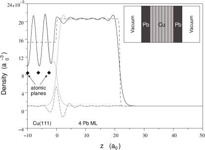
The main results of this paper are obtained with the pseudopotential generated in the previous section for the Cu(111) surface and the stabilized jellium model for the Pb overlayer. In the inset of Fig. 1 we sketch the geometry used in the calculations. In the middle there are 25 ML’s of Cu and Pb overlayers corresponding up to 23 ML’s (1 ML of Pb is 5.41 ) are attached symmetrically on both sides. Complementary calculations have been performed for unsupported Pb slabs, too.
Fig. 1 shows the electron and positive background densities corresponding to the coverage of 4 ML’s of Pb. We notice in the electron density in Pb six Friedel oscillations with the wavelength of about half Fermi wavelenght. In the present case they are produced by the 6th QWS band, the bottom of which has dropped well below the Fermi level. The 7th QWS band is still unoccupied. This kind of well-developed Friedel oscillation pattern commensurate with the thickness of the overlayer is characteristic for the stable “closed shell” or “magic” overlayer systems. In Cu(111) the electron density oscillates strongly, according to Fig. 1, as a consequence of the oscillating pseudopotential.
Fig. 1 gives also the electron densities of the corresponding free-standing Cu(111) and Pb slabs as dotted curves. It is remarkable that the electron density moves from Pb towards Cu(111), indicating a possible increase in the effective width of the Pb slab. The charge transfer obtained when comparing the Pb/Cu(111) system with its free-standing counterparts () reveals charge accumulation at the interface. A small amount of charge ( of one Pb ML charge) is transferred from Pb to Cu in order to equilibrate their chemical potentials, eV and eV for Pb and Cu, respectively. The charge transfer oscillates slightly as a function of the Pb slab thickness due to the oscillations in the Pb/Cu(111) Fermi level. These oscillations are in turn a consequence of the electron -confinement in the Pb overlayer.
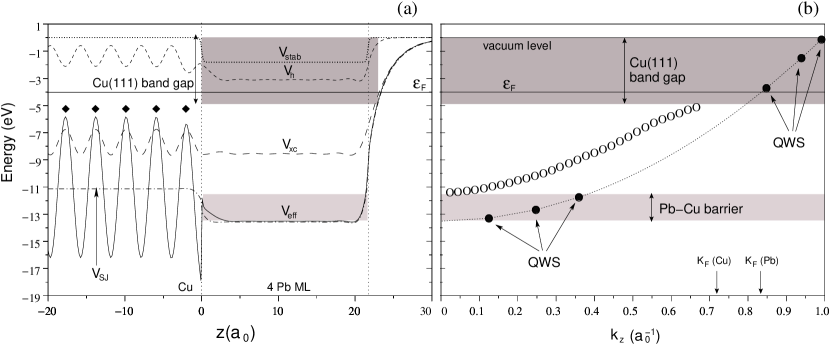
In Fig. 2(a) the effective potential and its components , and are shown; the total pseudopotential is not plotted for clearness. The effective potential corresponding to the same system, but modeled with the stabilized jellium for Cu, is also drawn (dash-dotted line), for comparison. Notice that it gives approximately the mean value of the Cu(111) pseudopotential. The dark gray shadowing gives the rough spatial extension where the localized QWS’s can appear because of the Cu(111) energy gap. The light gray area marks the potential well between the vacuum barrier and the Pb-Cu interface barrier. This well is created because the potential in Pb is 2 eV lower than the average Cu potential (notice the dash-dotted curve).
In Fig. 2(b) the eigenvalues are plotted as a function of the wavevector . Actually, as will be explained below, it is not a straightforward task to assign a wavevector to each state. Again, the dark gray area marks the position of the energy gap induced by the Cu(111) potential and the light gray area shows the lowest lying QWS’s bound by the Pb-Cu interface barrier. The QWS’s appearing in these energy regions are plotted with filled circles (Fig. 5 shows an example of the corresponding eigenfunctions (solid line)). The QWS’s fall on the parabola (dotted line) which is the free-electron-model band for Pb. The states extending over the whole Cu-Pb system and forming a continuous band are plotted with open circles. The nearly parabolic band reflects the free-electron character in our description of the Cu substrate. The QWS’s in the lower, light gray area are supposed to have a minor relevance on the electronic properties of the system. In contrast, QWS’s in the upper dark gray area play an important role, because increasing the Pb thickness lowers the QWS energy and they become occupied one by one.
The repeated occupation of new QWS’s as a function of the overlayer thickness produces oscillations in all the electronic properties. In particular, oscillations in the energy give rise to Pb overlayers of especial stability. We studied recently these ”magic” island heights using the present model for the electronic structures.Ogando et al. (2004a)
As pointed out above, we divide the eigenstates into QWS’s and bulk states. We use different methods to assign wavevectors for these two groups of states. For bulk states, of minor importance in this study, we use the particle-in-a-box wavevector , where is an integer and the box width. On the other hand, QWS’s are very localized in the Pb slab and we obtain their wavevectors from the confinement kinetic energy as . is the energy difference between the QWS energy eigenvalue and the average potential value around the center of the Pb slab. The wavelengths can be measured also from the eigenfunctions and similar values are obtained. Below, the vector turns out to be a relevant parameter when evaluating the phase shifts at the interfaces.
III.2 Determination of confinement barriers I
III.2.1 Comparison with the experiments
Scanning tunneling spectroscopy is capable of resolving energy levels of QWS’s. Nevertheless, the interpretation of the experimental results is still difficult.Yeh et al. (2004); Otero et al. (2000) The results obtained by our model provide a good tool to enlighten the problems encountered and to suggest a simple but realistic picture with relevant parameters.
Fig. 3 shows the calculated eigenvalues as a function of the number of Pb ML’s. The comparison with the QWS energy levels measured by Otero et al.Otero et al. (2000) shows a good agreement for large coverage heights. Below 6 ML’s the correspondence is a bit worse. This can be due to an inaccurate description of the Cu-Pb interface or due to the interaction with the Cu electrons omitted in the calculations. The importance of these phenomena decreases as the number of ML’s increases.
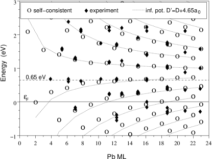
To explain the measured energy eigenvalues Otero et al.Otero et al. (2000) tried first the finite-square-potential-well model but the fit was not satisfactory. However, they obtained a very good agreement by using the infinite-square-potential-well model or by decreasing the width of the finite square well by . The fact that the infinite potential well produces much better results than the, in principle, more realistic finite potential well is counterintuitive, because it has been proven for slabs,Stratton (1965); Schulte (1976) wires Ogando et al. (2002); García-Martín et al. (1996) and clusters Brack (1993) that the real potential profiles are soft. In fact, it can be seen in Fig. 2a that the self-consistent potential is soft with an effective width increasing as a function of the QWS energy level. On the other hand, this effect seems not to be counterbalanced by the confining potential on the Cu-Pb interface. The QWS’s penetrate inside the Cu(111) (see Fig. 5) and the electron density in Fig. 1 moves towards Cu. Nevertheless, a very good agreement with the experiments is obtained with both the infinite-square-potential-well model and soft self-consistent potentials. In addition, in Fig. 3 we show the eigenvalues (linked by dotted curves) obtained with the infinite-square-potential-well model but by using well widths increased by in order to take into account the wavefunction spill-out. As can be seen, a good fit is obtained also in this way.
III.2.2 Calculation of the phase shifts
In order to clarify the reasons for these contradictions or dissimilar results, we use the phase-accumulation model and evaluate the phase shifts for the confinement barriers in our self-consistent calculations. We use the unsupported Pb slab to calculate the phase shift and then we can evaluate the phase shift in the Pb/Cu(111) system.
The procedure used is to choose a QWS with an energy just below the vacuum level and then to identify the corresponding quantum number . After the wavevector is calculated from the kinetic energy as explained at the end of Section III.1, the phase shift is evaluated for the QWS energy level by Eq. (6). Increasing the slab thickness, the energy eigenvalue decreases and we calculate as a function of the energy. The phase shift depends on the potential profile of the surface. Therefore we check that it remains unaltered for thicknesses over ML’s. Once has been calculated by using the unsupported Pb slab, the phase shift can be evaluated in the same way using the results of the Pb/Cu(111) system. Similarly to the above procedure for the phase shifts, we also determine, according to Eq. (7), the shifts in the surface and interface positions and , respectively.
The identification of the quantum number is easy for states in free-standing Pb slabs. But it is difficult for the QWS’s in the Pb/Cu(111) system because, in principle, it is not known how many states are hidden as resonances in the region of delocalized states in Cu (the white area between the gray ones in Fig. 2(b). Nevertheless, the local DOS integrated over the Pb overlayer reveals the number of the QWS resonances and, in addition, we have the possibility to plot the eigenfunctions in order to check the identification.

The dependences of the phase shifts on the energy eigenvalue are shown in Fig. 4. We notice that nearly in the whole energy range the phase shift at the Cu(111)-Pb interface is larger than that at the vacuum side. This means that the wavefunction penetration into Cu(111) is larger than the spill out into the vacuum. The behaviour of the phase shift can be compared with that obtained in the three-dimensional DFT calculations with more realistic atomic pseudopotentials. For example, the results by Wei and ChouWei and Chou (2002) are in a qualitative agreement with the preset ones.
The phase shifts of the image-potential model, Eq. (10), reproduce quite well our results with the exception of the energies close to the vacuum level. This is due to the exponential decay of the DFT potential into the vacuum. The empirical Eq. (11) gives good results at the Cu-Pb interface if one corrects for the known downward shift of . Pendry and Gurman (1975) The finite-square-potential-well model does not produce phase shifts in agreement with the self-consistent results.
We plot in Fig. 4(b) the shifts of the barriers in the infinite-square-potential-well model according to Eq. (7) as a function of the energy eigenvalue. In the energy window from -1 to 3 eV accessible in the STS measurements the effective width increases more at the Cu(111)-Pb interface than at the Pb-vacuum surface. The shift of the effective Pb-vacuum barrier is in agreement with the jellium-model calculations by StrattonStratton (1965) who obtained the average shift of between the bottom of the potential well (at -9.5 eV) and the Fermi level.
Combining the results of Fig. 4 and Eqs. (6) or (7), the eigenvalues in Fig. 3 are reproduced. (The energy eigenvalues have to be shifted downwards by the width 9.5 eV of the occupied energy band.) A good qualitative behaviour is obtained simply by using the mean effective width which is the ideal width increased by . The dotted curves in Fig. 3 link the eigenenergies calculated in this way.
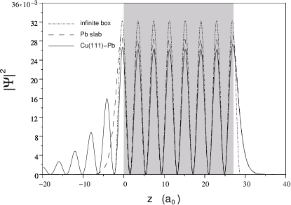
We compare in Fig. 5 our self-consistent DFT calculation for the Pb/Cu(111) system with two simple model calculations. There are 5 ML’s of Pb on the Cu(111) surface and we plot the electron density of the QWS at eV (solid line). The corresponding state in a free-standing Pb slab (dashed line) is obtained by shifting the left Pb-vacuum boundary by to the left in order to mimic the larger penetration of the wavefunctions into Cu(111) than into vacuum. The value of reproduces the correct infinite-barrier shift in Fig. 4(b). The eigenenergy of this Pb slab state is also 0.53 eV. On the right surface, of course, both wavefunctions overlap and at the left surface the slab wavefunction tries to mimic, without oscillations, the decay of the wavefunction in the Pb/Cu(111) system. The corresponding state calculated using the infinite-square-potential-well model with the appropriate shifts of the barriers ( and from Fig. 4(b)) is also given in Fig. 5 (dash-dotted line). Note that this simple model gives the correct energy eigenvalue and describes well the wavefunction inside Pb but it cannot account for the decay into the Cu substrate. In conclusion, the two simple models reproduce quite well the eigenfunctions inside Pb and at the Pb-vacuum barrier, but not beyond the Cu(111)-Pb interface. In order to describe properties related to the penetration of the wavefunctions into the substrate, the slab and infinite-square-potential-well models are inadequate.
III.2.3 Importance of quantum numbers
The model based on the phase shifts or on the effective width increase of the infinite potential well reproduces the eigenvalues and eigenfunctions of the self-consistent calculation. Because the self-consistently calculated eigenvalues agree with the experimental ones, Otero et al. (2000) the latter can be fitted with . Nevertheless, Otero et al. Otero et al. (2000) obtain a good agreement with .
To explain the contradiction we have compared the infinite-square-potential-well energy spectrum (Eq. (7) obtained with ) and our model results corresponding to . In the latter the quantum number for the eigenstates with the nearly constant eigenenergy of are for 2,4,6,…ML’s of Pb, respectively. Actually, this is in agreement with the pseudopotential calculations for free-standing Pb slabs. Wei and Chou (2002) But gives the corresponding quantum numbers as i.e., they are one unit smaller than the correct set. This explains why both models reproduce approximately the same experimental energy spectrum. The wavelength of the states at 0.65 eV in the infinite potential well is . When we increase the width of the well by the states lie exactly at the same energy. This does not hold for energies far from and the eigenenergy spectra become remarkably different. Nevertheless, in the narrow energy window from -1 to 3 eV scanned in experiments, the energy spectra of both models are very similar and fit quite well the experimental results. As a matter of fact, an even better fit of experiments seems to be obtained by increasing the width of the potential well by and using states with quantum numbers two units larger than in the original infinite-square-potential-well model.
In conclusion, the energy spectra can be fitted with several different thickness and quantum numbers. The danger is that other properties such as the wavefunctions or ”magic” heights are wrongly determined. For example, the correct determination of the physical parameters reveals crucial in the description of the envelope function which plays a key role in determining the energetics of the quantum well states Kawakami et al. (1999) or the magnetic coupling in multilayer structures.Ortega et al. (1993)
III.3 Determination of confinement barriers II
III.3.1 Calculation of from energy differences
The disadvantage of the previous method for determining the positions of the confining barriers is the necessity to measure a large number of QWS eigenenergies in order to label correctly the quantum states. However, there exists methods in which the knowlegde of the quantum number is not needed. Altfeder et al. (1997); Su et al. (2001a, b); Wei and Chou (2002) We now elaborate this kind of methods.
From the energy difference between two consecutive states, one can obtain an effective thickness of the infinite potential well as
| (12) |
Above, is the thickness of the positive background density of the overlayer slab or, in the case of experiments, the measured thickness. is a wavevector depending on and . As before, is the difference between the measured nominal value and the effective one confining the electrons. The latter takes into account, e.g., the effect of the electron spill out into the vacuum or into the substrate, the unknown thickness of the wetting layer, and effects due to stress or relaxation at the boundaries.
We consider QWS’s in overlayers of different thickness and within a given window, e.g. the QWS’s shown in Fig. 3. We write Eq. (12) as
| (13) |
Then, by plotting as a function of and by fitting a straight line to the data, the slope gives averaged over the energy window in question. For example, the theoretical data of Fig. 3 gives which corresponds to the kinetic energy of , i.e. an energy 1 eV above the Fermi level.
The original theoretical data and the fit are shown in Fig. 6 by the diamond markers and by the dashed straight line, respectively. We plot , instead of , as a function of . This is because we want to include the exact values and the results of Eq. (15) (see below). The intersection of the dashed straight line with the vertical axis gives . This value is much larger than the value obtained for the total shift of the potential barriers in Section III.2. Namely, at the energy of above the Fermi level we obtain from Fig. 4(b) that .
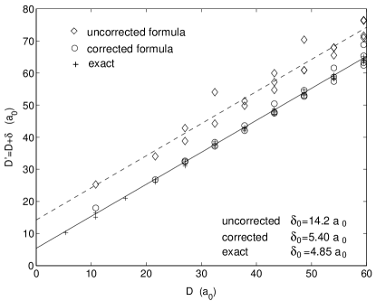

The method described above (Eq. (13)) has been used to determine the number of Pb wetting layers in the STS. Our finding that the method overestimates the distance between the confinement barriers may explain the large values Altfeder et al. (1997); Su et al. (2001a, b); Wei and Chou (2002) obtained by this scheme in comparison with other experiments. Yeh et al. (2004); Hupalo and Tringides (2002); Mans et al. (2002) The reason for this disagreement is the basic fact that Eqs. (12) and (13) correspond to the infinite potential well, whereas a finite potential well is closer to reality. The infinite-square-potential-well model with the shifts of the confining barriers reproduces quite accurately the energy spectrum as is demonstrated in Fig. 7. The figure shows that the infinite potential well with the thickness of 8ML+4.5 mimics the energy spectrum of a 8 ML unsupported Pb jellium slab. But the reasoning to the opposite direction, the determination of the value from the real energy spectrum cannot be done using the scheme. The explanation is that the energy eigenvalue differences between the consecutive states behave differently in the infinite-square-potential-well and in real systems. The inset of Fig. 7 shows that the infinite potential well results in a monotonically increasing whereas in the more realistic stabilized-jellium model decreases close to the vacuum level. The wrong trend in the infinite-square-potential-well model is compensated by the erroneously large effective width of the Pb slab or overlayer obtained by applying Eq. (13). In the next subsections we suggest a method purified from this effect.
III.3.2 Corrected formula for the calculation of
The option we choose to correct the overestimation inherent in Eq. (13) is to introduce the effect of the finite potential barrier. This can be done by assuming that the surface shift is energy-dependent as . Here, is the mean value we want to determine. Our aim is to obtain information about the electron confinement strength through the parameter, which is energy-independent but it is reproduces satisfactorily the energy spectrum (see Fig. 7). Nevertheless, it is necessary to use the energy-dependent function to obtain relevant values.
The energy difference between the successive states can be obtained to the first order as ( increases by unity). The energy derivative for a given thickness is
| (14) |
where is the energy derivative of the surface shift and it depends on energy. This equation has to be evaluated for a given . For the infinitely deep potential well and we do not recover the exact result of Eq. (12). This deficit can be corrected by evaluating the right-hand side of Eq. (14) at . The corresponding is also evaluated at using the self-consistent values shown in Fig. (4b). Then, rearranging the terms of Eq. (14) we obtain the corrected formula for the thickness as
| (15) |
Here, it is accurate enough to use the obtained previously with Eq. (12). Omitting the dependence of on energy on the right hand side of Eq. (15), i.e. , we can calculate the value of by fitting a straight line for as a function of .
The circles and the solid straight line in Fig. 6 give the values and the fit, respectively, corresponding to Eq. (15). The new mean value is consistent with the electron spill out shown in Fig. (4b) and it is much better than the value of obtained with the uncorrected formula (13). Namely, the exact values (shown as crosses in Fig. 4) give .
III.3.3 Analytic models for the correction
In order to apply the corrected scheme of the previous subsection the energy-dependent derivative has to be known. We study now the reliability of different analytical models in its estimation. These models allow us to extend the previous analysis to other substrates or overlayers without doing self-consistent electronic structure calculations.
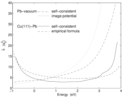
The finite-square-potential-well model does not provide a correction large enough, because the potential is not a continuous function of energy. The values are too small (see Fig. 4(a)). The image-potential model (Eq. (10)) and the empiric phase shifts (Eq. (11)) provides results in a much better agreement with experiments. We want to emphazise that even if the analytical phase shifts may not produce the same values as the self-consistent calculations (for example, due to the fact that the phase shift is determined with the module of ) they reproduce reasonably well the energy derivative needed in the correction in Eq. (15).
Fig. 8 shows the derivatives from the self-consistent calculation and from the analytical models of Sec. II.3. The agreement is quite good, even if the derivatives of the self-consistent calculation are generally smaller. Comparing self-consistent and analythical curves we notice that small differences in the phases (Fig. (4)) produce big differences in Fig. 8. As a matter of fact, at energies close to the vacuum the image-potential results could be more relevant than the self-consistent DFT results, which are affected by the exponential decay of the DFT potential. Because according to Fig. 8 the correction is large at energies close to the vacuum level and also close to the bottom of the projected energy gap of the substrate, we recommend the use of QWS’s at intermediate energies when determining the overlayer thickness.
| System | Up to | from Eq. (13) | from Eq. (15) | from Eq. (15) | Exact |
|---|---|---|---|---|---|
| uncorrected | numerical correction | analytical correction | |||
| Free-standing Pb | 10 ML | 12(3) | 5.5(0.6) | 6(3) | 3.9(0.3) |
| Pb/Cu(111) | 23ML | 12(1) | 5(2) | 3(2) | 4.7(0.1) |
| Pb/Cu(111) | 10ML | 13(1) | 6(1) | 4(2) | 4.8(0.3) |
| Experiments Otero et al. (2000) | 24ML | 15(5) | 7(5) | 5(5) | 4.0(0.2) |
| Na/Cu(111) | 20ML | 7(3) | 1(3) | 3(4) | 1.2(0.3) |
Table 1 shows a collection of values obtained for several systems using different approximations. In addition to our theoretical results for the Pb/Cu(111) and the free-standing Pb slab systems we analyze our similar results for Na/Cu(111) and the experimental QWS spectrum of Pb/Cu(111) [Otero et al., 2000]. The ”exact ” values are obtained by fitting a straight line through the exact results . In general, the uncorrected Eq. (13) gives for the Pb systems values nearly three times larger than the exact one. In contrast, the corrected value offers a sub-monolayer accuracy.
For the Na/Cu(111) system the difference between the corrected and uncorrected is large as well. Although the wavelength of Na is larger than for Pb, does not scale with it. The deeper potential of Cu(111) than the Na potential (the opposite to the Pb/Cu(111) system) shifts the barrier inside the Na, i.e. the value of is negative. This explains the small value of .
It is noticeable that applying Eq. (15) with the numerical and the analytical corrections to the experimental results of ref. [Otero et al., 2000] we obtain and , respectively. These values are much smaller than the uncorrected value of . When we compare with the exact value of , which is obtained by identifying first the quantum numbers. The linear regression error is anyway substantial. In addition to the errors due to our first-order approximation in Eq. (14), the experimental dispersion in the QWS spectrum cause uncertainty. In general, for self-consistent calculations the numerical correction provides better determination of compared to the analytical one. But in the case of the experimental data the analytical correction is better.
When analyzing experiments, the value obtained by the corrected scheme of Eq. (15) can be used as an initial parameter to determine the quantum number. Then, employing the exact equation to fit the energy spectrum, improved results are obtained.
IV Conclusions
We have performed self-consistent DFT calculations to study the confinement barriers of electrons in Pb islands grown on the Cu(111) substrate. Calculations have been done for free-standing Pb slabs and Pb slabs on Cu(111). Pb was described by stabilized jellium and the Cu(111) substrate by a 1D-pseudopotential. The model reproduces the most important physical properties and gives results in a good agreement with experiments.
The energies and wavefunctions of the quantum well states in the Pb slabs characterize the confinement barriers at the Pb-vacuum surface and at the Cu(111)-Pb interface. We have analyzed these states by using the phase accumulation model and by determining effective widths of infinite potential wells reproducing the energies. The Pb-vacuum phase shift is in a good agreement with more realistic pseudopotential calculations. The Cu(111)-Pb phase shift or the effective width of the potential well accounts for the confining strength of the Cu(111) energy gap. This strength is weaker than that of the Pb-vacuum barrier.
The information provided by our calculations and analysis allows to improve the interpretation of QWS spectra measured by scanning tunneling spectroscopy. More specifically, we have shown that a formula commonly used in the literature results easily in the overestimation of the effective width of the infinite potential well. We have offered an alternative expression to correct that deficiency, specially important for electronic high density (small ) metals. The obtained results can be used to estimate the width of the potential well and to determine the quantum numbers for a more accurate analysis of the confinement barriers.
Finally, the 1D-pseudopotential scheme provides a method for future studies of nanostructures on solid surfaces. Despite this work is focused on STS experiments and Pb/Cu(111) system, our results can be qualitatively applied to metallic nanoislands on semiconducting substrates, e.g. Pb or Ag on Si, as well as to photoemission experiments.
Acknowledgements.
The authors are grateful to R. Miranda for his valuable comments. We acknowledge partial support by the University of the Basque Country (9/UPV00224.310-14553/2002), the Basque Hezkuntza Unibertsitate eta Ikerkuntza Saila, and Spanish Ministerio de Ciencia y Tecnología (MAT 2001-0946 and MAT2002-04087-CO2-O1). This work was also partially supported by the Academy of Finland through its Centre of Excellence Program (2000-2005).References
- Ortega and Himpsel (1992) J. E. Ortega and F. J. Himpsel, Phys. Rev. Lett. 69, 844 (1992).
- Chiang (2000) T. C. Chiang, Surf. Sci. Rep. 39, 181 (2000).
- Otero et al. (2002) R. Otero, A. L. Vázquez de Parga, and R. Miranda, Phys. Rev. B 66, 115401 (2002).
- Hinch et al. (1989) B. J. Hinch, C. Koziol, J. P. Toennies, and G. Zhang, Europhys. Lett. 10, 341 (1989).
- Budde et al. (2000) K. Budde, E. Abram, V. Yeh, and M. C. Tringides, Phys. Rev. B 61, 10602 (2000).
- Luh et al. (2001) D. A. Luh, T. Miller, J. J. Paggel, M. Y. Chou, and T. C. Chiang, Science 292, 1131 (2001).
- Yeh et al. (2004) V. Yeh, M. Hupalo, E. H. Conrad, and M. C. Tringides, Surf. Sci. 551, 23 (2004).
- Hupalo and Tringides (2002) M. Hupalo and M. C. Tringides, Phys. Rev. B 65, 115406 (2002).
- Mans et al. (2002) A. Mans, J. H. Dil, A. R. H. F. Ettema, and H. H. Weitering, Phys. Rev. B 66, 195410 (2002).
- Hupalo et al. (2001) M. Hupalo, S. Kremmer, V. Yeh, L. Berbil-Bautista, E. Abram, and M. C. Tringides, Surf. Sci. 493, 526 (2001).
- Su et al. (2001a) W. B. Su, S. H. Chang, W. B. Jian, C. S. Chang, L. J. Chen, and T. T. Tsong, Phys. Rev. Lett. 86, 5116 (2001a).
- Menzel et al. (2003) A. Menzel, M. Kammler, E. H. Conrad, V. Yeh, M. Hupalo, and M. C. Tringides, Phys. Rev. B. 67, 165314 (2003).
- Ogando et al. (2004a) E. Ogando, N. Zabala, E. V. Chulkov, and M. J. Puska, Phys. Rev. B. 69, 153410 (2004a).
- Gavioli et al. (1999) L. Gavioli, K. R. Kimberlin, M. C. Tringides, J. F. Wendelken, and Z. Zhang, Phys. Rev. Lett. 82, 129 (1999).
- Matsuda et al. (2004) I. Matsuda, H. W. Yeom, T. Tanikawa, K. Tono, T. Nagao, S. Hasegawa, and T. Ohta, Phys. Rev. B 63, 125325 (2004).
- Nagao et al. (2004) T. Nagao, J. T. Sadowoski, M. Saito, S. Yaginuma, T. Kogure, Y. Fujikawa, T. Ohno, S. Hasegawa, and T. Sakurai, Phys. Rev. Lett. (2004), accepted.
- Czoschke et al. (2003) P. Czoschke, H. Hong, L. Basile, and T. C. Chiang, Phys. Rev. Lett. 91, 226801 (2003).
- Floreano et al. (2004) L. Floreano, D. Cvetko, F. Bruno, G. Bavdek, A. Cossaro, R. Gotter, A. Verdini, and A. Morgante, Prog. Surf. Sci. 72, 135 (2004).
- Otero et al. (2000) R. Otero, A. L. Vázquez de Parga, and R. Miranda, Surf. Sci. 447, 143 (2000).
- Altfeder et al. (1997) I. B. Altfeder, K. A. Matveev, and D. M. Chen, Phys. Rev. Lett. 78, 2815 (1997).
- Su et al. (2001b) W. B. Su, S. H. Chang, C. S. Chang, L. J. Chen, and T. T. Tsong, Jpn. J. Appl. Phys. 40, 4299 (2001b).
- Wei and Chou (2002) C. M. Wei and M. Y. Chou, Phys. Rev. B 66, 233408 (2002).
- Materzanini et al. (2001) G. Materzanini, P. Saalfrank, and P. J. D. Lindan, Phys. Rev. B 63, 235405 (2001).
- Feibelman (1983) P. J. Feibelman, Phys. Rev. B. 27, 1991 (1983).
- Feibelman and Hamann (1984) P. J. Feibelman and D. R. Hamann, Phys. Rev. B. 29, 6463 (1984).
- Kiejna et al. (1999) A. Kiejna, J. Peisert, and P. Scharoch, Surf. Sci. 432, 54 (1999).
- Boettger and Trickey (1992) J. C. Boettger and S. B. Trickey, Phys. Rev. B 45, 1363 (1992).
- Boettger (1996) J. C. Boettger, Phys. Rev. B 53, 13133 (1996).
- Saalfrank (1992) P. Saalfrank, Surf. Sci. 274, 449 (1992).
- Batra et al. (1986) I. P. Batra, S. Ciraci, G. P. Srivastava, J. S. Nelson, and C. Y. Fong, Phys. Rev. B 34, 8246 (1986).
- Schulte (1976) F. K. Schulte, Surf. Sci. 55, 427 (1976).
- Sarría et al. (2000) I. Sarría, C. Henriques, C. Fiolhais, and J. M. Pitarke, Phys. Rev. B. 62, 1699 (2000).
- Fiolhais et al. (2001) C. Fiolhais, C. Henriques, I. Sarría, and J. M. Pitarke, Prog. Surf. Sci. 67, 285 (2001).
- Wojciechowski and Bogdanów (1998) K. F. Wojciechowski and H. Bogdanów, Surf. Sci. 397, 53 (1998).
- Ciraci and Batra (1986) S. Ciraci and I. P. Batra, Phys. Rev. B 33, 4294 (1986).
- Hong et al. (2003) H. Hong, C. M. Wei, M. Y. Chou, Z. Wu, L. Basile, H. Chen, M. Holt, and T. C. Chiang, Phys. Rev. Lett. 90, 076104 (2003).
- Echenique and Pendry (1978) P. M. Echenique and J. B. Pendry, J. Phys. C 11, 2065 (1978).
- Jones and Gunnarsson (1989) R. O. Jones and O. Gunnarsson, Rev. Mod. Phys. 61, 689 (1989).
- Wang and Perdew (1991) Y. Wang and J. P. Perdew, Phys. Rev. B 43, 8911 (1991).
- Ceperley and Alder (1980) D. M. Ceperley and B. J. Alder, Phys. Rev. Lett. 45, 566 (1980).
- Mandel and McCormick (1989) J. Mandel and S. F. McCormick, J. Comput. Phys. 80, 442 (1989).
- Heiskanen et al. (2001) M. Heiskanen, T. Torsti, M. J. Puska, and R. M. Nieminen, Phys. Rev. B 63, 245106 (2001).
- Torsti et al. (2003) T. Torsti, M. Heiskanen, M. J. Puska, and R. M. Nieminen, Int. J. Quantum Chem. 91, 171 (2003).
- Perdew et al. (1990) J. P. Perdew, H. Q. Tran, and E. D. Smith, Phys. Rev. B 42, 11627 (1990).
- Shore and Rose (1991) H. B. Shore and J. H. Rose, Phys. Rev. Lett. 66, 2519 (1991).
- Chulkov et al. (1999) E. V. Chulkov, V. M. Silkin, and P. M. Echenique, Surf. Sci. 437, 330 (1999).
- Chulkov et al. (1997) E. V. Chulkov, V. M. Silkin, and P. M. Echenique, Surf. Sci. 391, L1217 (1997).
- Chulkov et al. (1998) E. V. Chulkov, I. Sarría, V. M. Silkin, J. M. Pitarke, and P. M. Echenique, Phys. Rev. Lett. 80, 4947 (1998).
- Ogando et al. (2004b) E. Ogando, N. Zabala, E. V. Chulkov, and M. J. Puska (2004b), unpublished.
- Smith (1985) N. V. Smith, Phys. Rev. B 32, 3549 (1985).
- Echenique and Pendry (1989) P. M. Echenique and J. B. Pendry, Prog. Surf. Sci. 32, 111 (1989).
- Stratton (1965) R. Stratton, Phys. Lett. 19, 556 (1965).
- Ogando et al. (2002) E. Ogando, N. Zabala, and M. J. Puska, Nanotechnology 13, 363 (2002).
- García-Martín et al. (1996) A. García-Martín, J. A. Torres, and J. J. Sáenz, Phys. Rev. B 54, 13448 (1996).
- Brack (1993) M. Brack, Rev. Mod. Phys. 65, 677 (1993).
- Pendry and Gurman (1975) J. B. Pendry and S. J. Gurman, Surf. Sci. 49, 87 (1975).
- Kawakami et al. (1999) R. K. Kawakami, E. Rotenberg, H. J. Choi, E. J. Escorcia-Aparicio, M. O. Bowen, J. H. Wolfe, E. Arenholz, Z. D. Zhang, N. V. Smith, and Z. Q. Qiu, Nature 398, 132 (1999).
- Ortega et al. (1993) J. E. Ortega, F. J. Himpsel, G. J. Mankey, and R. F. Willis, Phys. Rev. B. 47, 1540 (1993).