Multilayers of Zinc-Blende Half-Metals with Semiconductors
Abstract
We report on first-principles calculations of multilayers of zinc-blende half-metallic ferromagnets CrAs and CrSb with III-V and II-VI semiconductors, in the [001] orientation. We examine the ideal and tetragonalised structures, as well as the case of an intermixed interface. We find that, as a rule, half-metallicity can be conserved throughout the heterostructures, provided that the character of the local coordination and bonding is not disturbed. At the interfaces with semiconductors, we describe a mechanism that can give also a non-integer spin moment per interface transition atom, and derive a simple rule to evaluate it.
pacs:
71.20.Be, 71.20.Lp, 75.50.Cc1 Introduction
Half-metallicity is the property of some spin polarised materials to exhibit a metallic density of states for one spin direction but a clear band gap around the Fermi level for the other [1]. Well known half metals are some Heusler alloys [1, 2, 3, 4], the compound CrO2 [5], the manganite La0.7Sr0.3MnO3 [6], magnetite (Fe3O4) [7] or some diluted magnetic semiconductors (DMS) [8]. In recent years technological interest in possible applications on spin-dependent transport has fueled the research in this field. For instance, ordered zinc-blende CrAs and CrSb have been fabricated by molecular beam epitaxy, and experiment and calculations suggest half-metallicity [9, 10]. The high Curie temperature (over 400 K in experiment [11, 12] and in theory [13]) makes these compounds attractive also for applications. CrAs/GaAs [10] and CrSb/GaAs [14] multilayers have been also realised, showing that coherent heterostructures are possible.
Such zinc-blende compounds of transition elements with group-V and VI atoms (called pnictides and chalcogenides) have been also studied by ab-initio methods. Calculations of the total energy and structural optimisation agree with the experimental result that the ground state structure of such compounds is not the zinc-blende, but in most cases the NiAs structure [15]—rather more complicated and certainly not half-metallic [16, 17, 18, 19, 20]. The zinc-blende structure can only be achieved by epitaxial growth on semiconductors for a few monolayers. Heterostructures of half-metals with semiconductors are technologically interesting, since in principle they can be used to achieve spin injection from the ferromagnetic electrode to the semiconductor with 100 % spin polarised current, a very useful quality for potential application in spin transistors [21].
Until now, among the high- half-metals, heterostructures of Heusler alloys with semiconductors have been found to suffer from interface states within the half-metallic gap [22, 23], which can strongly reduce the spin polarisation of the current. On the other hand, zinc-blende half-metals follow the structure and the bonding of the zinc-blende semiconductors in a more coherent way, and thus one can expect to avoid spurious interface states. Motivated by these ideas, we investigate in this paper the half-metal/semiconductor (HM/SC) contact for the zinc-blende materials and see under which conditions half-metallicity is preserved; moreover, we investigate the magnetic moments at the interface.
The paper is organised as follows: In section 2 we give a few details on our calculations. In section 3 we shortly review the bulk properties of these half-metallic compounds, and address the effect of lattice distortion by tetragonalisation. In section 4 we present calculations on HM/SC multilayers in ideal geometry and epitaxy and see in which cases half-metallicity is preserved. In section 5 we examine interdiffusion effects at the interface and in section 6 we discuss the spin magnetic moments at the interface. Finally, we conclude with a summary in section 7.
2 Method of calculation
Our calculations are based on density-functional theory within the local density approximation (LDA) for the exchange-correlation potential, with the Vosko, Wilk and Nusair parameterisation [24]. We employ the full-potential screened Korringa-Kohn-Rostoker (KKR) Green function method [25], where the correct shape of the Wigner-Seitz cells is taken [26]. For the calculation of the charge and spin density we integrate along a contour on the complex energy plane, which extends from below the valence states of the atom up to the Fermi level, using 42 energy points; the lower states are treated as atomic core states. For the Brillouin zone (BZ) integration we have used a k-space grid of 303030 in the full BZ for the bulk calculations and a -space grid 2020 in the two-dimensional full BZ for the interface calculations. We have used a cutoff of =3 for the wavefuctions and Green functions. More details are given in reference [27]. The calculations are performed within the scalar relativistic approximation, which accounts for relativistic effects other than the spin-orbit coupling. The effect of the latter on the half-metallic property is quite small for CrAs and CrSb, as shown in reference [28] (the reduction of the spin polarisation at the Fermi level is of the order of 0.5% for CrAs and 1.5% for CrSb).
3 Bulk properties
3.1 Ideal zinc-blende structure
The bulk properties of zinc-blende half-metals have been discussed in many papers in the past [17, 18, 19, 20, 27, 32, 33, 34, 35, 36, 37, 38, 39, 40, 41, 42]. Here we will summarise what is already known, and use this as a step towards the understanding of the bulk properties under tetragonal distortion and of the interface properties.
In the zinc-blende structure every atom has tetrahedral coordination, with its first neighbours being of the other atomic species. This symmetry splits the states of the transition-metal element (TM) in two subspaces: the with 3-fold degeneracy (, , and orbitals) and the with 2-fold degeneracy ( and ). The states of the TM hybridise with the states of the neighbouring atom (group V or VI), forming hybrids of bonding (lower in energy) and antibonding (higher) nature. This hybridisation and bonding-antibonding splitting is crucial for the formation of the gap in these compounds, and it is a characteristic of the tetrahedral coordination — in the hexagonal coordination of the energetically more stable NiAs structure, for instance, it is not present. The effect is already known as “- repulsion” in TM impurities in zinc-blende semiconductors [43].
The hybrids form wide bands, which retain the bonding-antibonding character and are therefore accordingly separated in energy. On the other hand, the orbitals are practically non-bonding and form narrow bands, which remain energetically between the bonding and antibonding states, separated from both. Meanwhile, the states of the TM are still higher in energy, pretty much like the state of the Ga atom in GaAs stays above . Only in cases of heavy anions, which have reduced ionicity, do these states come closer to but still stay above it for minority spin—see for instance a recent study on MnBi [44]. The states of the anion, on the other hand, are anyhow very low, lower than the bonding - hybrids.
This energetical separation already creates a band gap, and is assisted strongly by the exchange splitting due to spin magnetism. Thus, after the low-lying bonding bands are filled, the bands of only majority spin are progressively filled, while the corresponding minority bands are pushed higher above by the exchange splitting. As we change the valence of the TM atom toward the right in the periodic table, more majority bands are filled; the magnetic moment increases; thus the exchange splitting also increases keeping the minority states high in energy. In this way remains between the well-separated bonding bands and the bands, within a band gap. As a typical example we present the band structure of CrSb in figure 1 (left) for energies around the gap.
The situation described above changes when the lattice is compressed. Then the extended majority spin states of character feel the volume reduction and push higher, so that in the end enters the minority spin conduction band. After this point, although the gap still exists, it is below and half-metallicity is lost. Therefore it is necessary to identify which compounds are half-metallic in their equilibrium lattice parameter, and of course on which semiconductors they might grow. In reference [27] we have identified such systems, and we summarise the most important results here in table 1.
3.2 Tetragonal distortion of the zinc-blende structure
When a zinc-blende half-metallic compound is grown on a semiconductor substrate (say on (001)), its lattice will be tetragonally distorted so that it can assume the in-plane lattice constant of the SC while approximately keeping its own atomic volume. If the lattice match is good enough, the distortion will be minimal, and the electronic structure will change only slightly. Here we shall investigate this effect for the case of reasonable HM/SC lattice matching, in order to show that half-metallicity is not destroyed by moderate tetragonalisation.
As a model system for the discussion we choose CrSb, which we assume to be deposited on ZnTe (001) and to have taken the corresponding in-plane lattice parameter of the semiconductor aZnTe=6.1 Å and otherwise to have kept the atomic volume. This gives a ratio a=0.914, where is the lattice parameter in the growth direction. The corresponding band structure is shown in figure 1 (right). Comparing to the CrSb bands in the ideal zinc-blende geometry (figure 1 (left)), we see that the threefold degeneracy of the states at has split up into two subspaces, one singly (-) and one doubly degenerated (- and -). Also the representation at has split in its constituents, and . This behavior is expected because the axis is now distinguished. Evidently half-metallicity is preserved by this moderate distortion.
Such behavior is typical for all HM examined here. The tetragonalisation can have an effect on half-metallicity if is at the edge of the gap for the ideal structure. Then mainly the extended states, feeling the lateral change, will push higher, similarly to the case of lattice compression; ultimately, if the distortion is too large, half-metallicity can be destroyed. In particular, if the states are squeezed and move higher in energy, while if this happens to the and states.
4 HM/SC multilayers
In a recent examination of possible combinations of the transition elements V, Cr, and Mn, with group-V and VI elements [27], we found that some of them are half-metallic at their equilibrium lattice constants, which fit also reasonably well to those of some semiconductors (SC). Here we examine the cases of CrAs/SC and CrSb/SC (001) multilayers for which the lattice mismatch should be small, as can be seen from table 1. Note that within the LDA the lattice constant is usually underestimated by up to 2-4% [45]. Thus, if one allows for such a small increase of the calculated values of table 1 for the HM lattice constants, plus a moderate adjustment due to lattice mismatch, one arrives at the HM/SC combinations examined here.
We assume that the structures have the experimental SC lattice constant and that the ideal zinc-blende structure is kept throughout. The systems consist of 4 monolayers (ML) of HM followed by 4 ML of SC and periodically repeated, in accordance with the experimental result that only a few ML can exist within the periodically repeated supercell in the CrAs/GaAs case [10]. In the 001 direction of growth, this corresponds to interchanging monoatomic layers: e.g., for CrAs/GaAs, we have a supercell of the form …Cr/As/Cr/As/Ga/As/Ga/As… . For test purposes we have performed calculations on 8ML HM/8ML SC, and seen that our conclusions remain unchanged.
Our results on the the local DOS (LDOS) are presented in figure 2 for CrAs/GaAs (left) and for CrSb/InAs (right). In the multilayers we see that half-metallicity is conserved throughout. This means that no interface states within the gap are formed for the minority spin at the HM/SC interface. This can be understood since the growth is coherent, so that the local environment of the interface Cr atoms is not changed in CrAs/GaAs (This is also the case in CrAs/MnAs multilayers; see, e.g., reference [35]). In CrSb/InAs each interface Cr atom has two Sb neighbours on the one side and two As neighbours on the other, but the minority gap remains, since the - hybridisation and the bonding-antibonding splitting are still realised (the difference between having an As neighbour instead of an Sb one is that the states of the former are somewhat lower in energy).
For the majority spin the local DOS at decays within the SC layers. For a thick SC spacer it should vanish far from the interface, since the SC band gap is present and the DOS comes from exponentially decaying metal-induced gap states.
The main difference between the CrAs/GaAs multilayer and the CrSb/InAs one is the position of within the minority gap. In CrAs/GaAs, just touches the conduction band, while for CrSb/InAs it is lower, closer to the middle of the gap. This is a volume effect, clear also in the bulk CrAs case. The reduced lattice constant of CrAs/GaAs compared to CrSb/InAs affects the position of the within CrAs: the electrons feel the reduced volume and shift towards higher energy, pushing also .
Next we present the multilayer CrSb/ZnTe. We can call this a “mixed valence” multilayer, because it combines a 3d/group-V HM with a II/VI semiconductor. Thus, the environment of the interface Cr atom is highly anisotropic: on the one side it has two Sb neighbours and on the other two Te neighbours, the electronegativity of which is higher than Sb. Nevertheless, half-metallicity survives, since the - repulsion creating the bonding-antibonding splitting is still there, (although with different strength between Cr-Sb and Cr-Te), and the strong exchange splitting is of course also present. The half-metallic LDOS is shown in figure 3 (left).
However, there are two inequivalent ways to construct the multilayer, accounting for two different possible interfaces. The first is Cr/Sb/Cr/Te/Zn/Te/Zn/Te, which is the half metallic one presented in figure 3 (left), and the second is Cr/Sb/Cr/Sb/Zn/Te/Zn/Te, the difference being that here a Sb/Zn contact is present, i.e., a III-VI hybrid. In the latter case half-metallicity is destroyed, due to interface states which occur at the Sb/Zn interface at for the minority spin LDOS. The corresponding LDOS is shown in figure 3 (right), where the minority-spin interface states are formed at for the Sb (4) and Te (5) atoms. Similarly, only the Cr/Te/Cr/As/In/As/In/As stacking would retain half-metallicity in the case of a CrTe/InAs system, since in the case of the Cr/Te/Cr/Te/In/As/In/As stacking an In/Te interface is present.
Closing this section, we note that in the case of interfaces of half-metallic Heusler alloys with SC, the half-metallic gap is usually destroyed [22, 23, 46], e.g. from all the (theoretically) studied cases in reference [22] only the NiMnSb(111)/CdS(111) interface retained the half-metallicity, and this only when the interface was between the Sb and S atoms. Here, on the contrary, the HM gap is, as a rule, present, since the nature of the bonding is continued coherently at the interface.
5 Intermixed interface
Up to now we have considered only the ideal interface, without interdiffusion. However, in an experiment one can imagine that some intermixing can occur, and the question of keeping half-metallicity is raised again. As before, this can be discussed in terms of the bonding character.
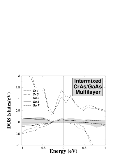
Consider, for instance, the CrAs/GaAs (001) interface, with an intermixed CrGa monolayer (i.e., a layer sequence of …Cr/As/Cr0.5Ga0.5/As/Ga/…), under the assumption that the tetrahedral cation-anion coordination is not severely distorted (this is a necessary requirement in all considerations of half-metallicity in these materials). Then, the first neighbours of each interface Cr atom will be As atoms, and the same holds for the neighbours of the Ga atoms. A Cr-Ga bond will not be present, since the closest distance between Cr and Ga atoms is the one of second neighbours. Thus we expect the same bonding-antibonding scheme as before, so that the HM gap should remain. Changes will occur, of course, for example due to the different electrostatic potential at the interface, since Cr and Ga gave different ionicity. Thus can be shifted with respect to the ideal interface.
In order to investigate if the HM property is really preserved, we performed a calculation of such an intermixed interface, by constructing an in-plane supercell, double in size than the usual cell and containing one Cr and one Ga atom at the interface. The DOS in the vicinity of is shown in figure 4. Evidently, the system is half-metallic.
6 Magnetic moments
In the bulk HM, the total spin moment per unit cell is integer (in ), as follows from just noticing that, due to the gap at , the number of minority-spin electrons is an integer. This line of thinking leads to a simple “rule of 8” [27] connecting the total number of valence electrons of the unit cell and the total spin moment per unit cell:
| (1) |
since one has a total of 8 electrons in the bonding - bands and in the (deeper-lying) band of the element, and the remaining the electrons occupy only majority states and build up the magnetic moment. This “rule of 8” is generally valid for the whole family of zinc-blende half-metallic compounds, expressing a Slater-Pauling behaviour; similar rules hold also for the Heusler alloys [2, 3, 4] or HM superlattices [35]. As regards to the distribution of the spin moment among the atoms, the element has an induced moment opposite to the one of the transition element (thus for the local moment of the transition atom we have ). This can be understood in terms of the local character of the occupied bonding-- majority and minority bands (majority are more -like around the transition atom; minority are more -like around the atom). For details we refer to reference [27]. Here we discuss the magnetic moments of the multilayers and interfaces.
Since at the interface the translational symmetry is broken, the magnetic moment per transition atom is no longer obliged to be an integer, even if half-metallicity is preserved. This has been already observed in the case of (001) surfaces [27]. In the case of a transition-atom-terminated interface with a SC, the total moment per interface transition atom depends on the valency of its neighbours on each side. To understand this, it is convenient to consider the occupied bonding - hybrids plus the low-lying states of the atom as a kind of “reservoir” which has space for electrons (both spin directions are occupied), and to count the electrons which fill it up; once the state reservoir is filled, the remaining electrons will occupy only majority-spin states ( and - antibonding) and build up the moment. Every neighbour of the TM introduces thus 8 low-lying states, and at the same time valence electrons; this adds up to a total of unfilled reservoir states, or holes, to absorb the TM electrons. On the other hand, each one of these neighbours has a total of 4 neighbours itself, thus it contributes only of its states to the particular TM. Adding these up, we find a modified “rule of 8”, applicable for the total spin moment per interface or surface TM in zinc-blende half-metals provided that half-metallicity is preserved at the interface or the surface (eq. (1) is a special case of this):
| (2) |
Here, is the number of neighbours, which will be less than 4 in the case of a surface TM. As in the case of eq. (1), this simple rule applies only when half-metallicity is present. The moment found by this rule is not expected to be completely localised at the TM, but rather distributed among the TM and the surrounding sites.
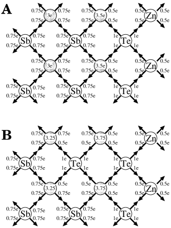
The situation is illustrated schematically in figure 5A for the case of ZnTe/CrSb (in the figure we do not discuss the states of the Sb and Te atoms, since they are energetically low-lying and already filled by two electrons). In the bulk, each Sb neighbour of the Cr atom gives 3/4 of an electron to the - bond, so that the 4 Sb neighbours give a total of 3 electrons per Cr atom. At the ZnTe/CrSb interface the Cr atom has two Sb and two Te neighbours. The Sb ones give again 3/4 of an electron each, while the Te give one electron each (since they have one more valence electron). Adding these up, we have a total of 3.5 donated by the atoms to partly fill the bonding states of the interface Cr atom. Since there are 6 such states, the remaining 2.5 are donated by the Cr atom, while the magnetic moment is built up by the remaining electrons of Cr, where is the valence of Cr. As a result, a half-integer moment of per interface Cr atom occurs. In fact, this cannot be strictly localised at the interface, but is distributed among the interface atoms and their neighbours.
Note that the above sum rules refer only to the total moments, but not to the local ones. For instance, table 2 gives the local spin moments for the half-metallic multilayers. In comparing CrAs/GaAS (total interface moment: 3 ) with CrSb/ZnTe (total interface moment: 3.5 ) results we find that the local interface Cr moment increases by about 0.45 and the other 0.05 is achieved by a reduction of the absolute value of the negative anion moments; interface Te atoms have a spin moment of around -0.06 compared to the -0.10 of the As interface atoms. In the case of the CrSb/InAs system the total interface moment should be 3 as for CrAs/GaAs and the larger Cr moment at the interface for the former system is compensated by the larger absolute values of the spin moments of the anions. The difference between the two systems arises mainly due to the larger electronegativity of As compared to Sb. The As states are originally lower than the Sb ones, so that the - hybridisation is weaker, and the bonding states of majority spin are more localised around the As atom; thus the absolute value of both Cr and As moments is smaller.
But it is also possible to obtain a value of or per Cr atom. Such an example is shown schematically in figure 5B, where we have substituted the pure Sb layer at the interface by a Sb0.5Te0.5 intermixed layer. Each Cr atom at the interface has one Sb and three Te atoms as first neighbours, and gives away 2.25 electrons to the bonding states. Thus electrons are left to build up the spin moment. Similarly the Cr atoms in the sub-interface layer have now three Sb and one Te atoms as first neighbours and a total spin moment of .
The above sum rule can be considered as a generalisation of the sum rule derived in reference [27] for the surfaces. In the case of the Cr-terminated CrAs(001) or CrSe(001) surfaces, the Cr atom at the interface loses two of its four neighbours and its spin moment is increased by 1.5 in the case of the CrAs(001) surface and by 1.0 for the CrSe(001) surface.
7 Summary and conclusions
We have performed first-principles calculations of (001) multilayers of half-metallic zinc-blende compounds (CrAs and CrSb) with III-V and II-VI semiconductors, focusing on the question whether half-metallicity is conserved at the interface. We have found that this can be the case under not too restrictive assumptions.
Basically, the important requirement is that the coordination of the transition metal does not change at the interface: it should have four neighbours of anionic (electronegative) character, as in the bulk. Then the bonding-antibonding splitting of the - hybrides is retained and half-metallicity is conserved. It is not important that all four neighbours be of the same type. Thus, even in the InAs/CrSb and ZnTe/CrSb interfaces one observes half-metallicity. For the same reason, the intermixed Cr-Ga interface is half-metallic, too. We have also found that a moderate tetragonalisation does not affect the half-metallic character of the materials, thus growth of these half-metals on semiconductors with slightly different lattice constant brings no problems.
We have also examined the magnetic moments at the interface. We have found that, in the case of an interface between a TM/group-V compound and a II-VI semiconductor, the total spin magnetic moment at the interface has a non-integer value. Based on simple arguments, applicable to any zinc-blende ferromagnetic surface or interface provided that half-metallicity is preserved, we have derived a sum rule (eq. 2) to calculate this spin moment.
We conclude that zinc-blende half-metallic compounds combine various qualities desirable for spintronics applications: half-metallic ferromagnetism, high Curie temperatures, coherent growth and half-metallic interfaces with semiconductors. We hope that our work is motivating for further experimental research in the field.
References
References
- [1] de Groot R A, Mueller F M, van Engen P G and Buschow K H J 1983 Phys. Rev. Lett.50 2024
- [2] Galanakis I, Dederichs P H and Papanikolaou N 2002 Phys. Rev.B 66 134428
- [3] Galanakis I, Dederichs P H and Papanikolaou N 2002 Phys. Rev.B 66 174429
- [4] Galanakis I (unpublished); preprint in arXiv:cond-mat/0305134
- [5] Schwarz K J. Phys. F: Met. Phys.1986 16 L211; Korotin M A, Anisimov V I, Khomskii D I and Sawatzky G A 1998 Phys. Rev. Lett.80 4305
- [6] Soulen Jr R J, Byers J M, Osofsky M S, Nadgorny B, Ambrose T, Cheng S F, Broussard P R, Tanaka C T, Nowak J, Moodera J S, Barry Q and Coey J M D 1998 Science 282 85
- [7] Yanase A and Siratori K 1984 J. Phys. Soc. Jpn 53 312
- [8] Akai H 1998 Phys. Rev. Lett.81 3002
- [9] Akinaga H, Manago T and Shirai M 2000 Japan. J. Appl. Phys.39 L1118
- [10] Mizuguchi M, Akinaga H, Manago T, Ono K, Oshima M and Shirai M 2002 J. Magn. Magn. Mater.239 269
- [11] Zhao J H, Matsukura F, Takamura K, Abe E, Chiba D and Ohno H 2001 Appl. Phys. Lett. 79 2776
- [12] Mizuguchi M, Akinaga H, Manago T, Ono K, Oshima M, Shirai M, Yuri M, Lin H J, Hsieh H H and Chen C T 2002 J. Appl. Phys.91 7917
- [13] Kübler J 2003 Phys. Rev.B 67 220403
- [14] Zhao J H, Matsukura F, Takamura K, Chiba D, Ohno Y , Ohtani K and Ohno H 2004 Materials Science in Semiconductor Processing in press
- [15] Landolt-Börnstein, New Series, Group III, Vol. 27, Pt.a edited by K Adachi and S Ogawa (Springer-Verlag, Heidelberg) 1988
- [16] Wei S H and Zunger A 1987 Phys. Rev.B 35 2340
- [17] Sanvito S and Hill N A 2000 Phys. Rev.B 62 15553
- [18] Continenza A, Picozzi S, Geng W T and Freeman A J 2001 Phys. Rev.B 64 085204
- [19] Zhao Y J, Geng W T, Freeman A J and Delley B 2002 Phys. Rev.B 65 113202
- [20] Wen-Hui Xie, Ya-Qiong Xu, Bang-Gui Liu and Pettifor D G 2003 Phys. Rev. Lett.91 037204
- [21] Datta S and Das B 1990 Appl. Phys. Lett. 56 665
- [22] Wijs G A and de Groot R A 2001 Phys. Rev.B 64 R020402
- [23] Picozzi S, Continenza A and Freeman A J 2003 J. Phys. Chem. Solids 64 1697; ibid 2003 J. Appl. Phys.94 4723; Debernardi A, Peressi M and Baldereshi A 2003 Mat. Sci. Eng. C 23 743
- [24] Vosko S H, Wilk L and Nusair N 1980 Can. J. Phys.58 1200
- [25] Papanikolaou N, Zeller R and Dederichs P H 2002 J. Phys.: Condens. Matter14 2799
- [26] Stefanou N, Akai H and Zeller R 1990 Comp. Phys. Commun. 60 231; Stefanou N and Zeller R 1991 J. Phys.: Condens. Matter3 7599
- [27] Galanakis I and Mavropoulos Ph 2003 Phys. Rev.B 67 104417
- [28] Mavropoulos Ph, Sato K, Zeller R, Dederichs P H, Popescu V and Ebert H 2004 Phys. Rev.B 69, 054424
- [29] Landolt-Börnstein, New Series, Group III, Vol. 17, Pt.a edited by O Madelung (Springer-Verlag, Berlin) 1982
- [30] Landolt-Börnstein, New Series, Group III, Vol. 22, Pt.a edited by O Madelung (Springer-Verlag, Berlin) 1986
- [31] Landolt-Börnstein, New Series, Group III, Vol. 41, Pt.A1a edited by U Rössler, (Springer-Verlag, Berlin) 2001
- [32] Shirai M 2001 Physica E 10 143
- [33] Galanakis I 2002 Phys. Rev.B 66 012406
- [34] Zhang M, Hu H, Liu Z, Liu G, Cui Y and Wu G 2004 J. Magn. Magn. Mater.270 32
- [35] Fong C Y, Qian M C, Pask J E, Yang L H and Dag S 2004 Appl. Phys. Lett. 84 239
- [36] Wen-Hui Xie, Bang-Gui Liu and Pettifor D G 2003 Phys. Rev.B 68 134407
- [37] Bang-Gui Liu 2003 Phys. Rev.B 67 172411
- [38] Pask J E, Yang L H, Fong C Y, Pickett W E and Dag S 2003 Phys. Rev.B 67 224420
- [39] Sanyal B, Bergqvist L and Eriksson O 2003 Phys. Rev.B 68 054417
- [40] Wen-Hui Xie and Bang-Gui Liu 2003 J. Phys.: Condens. Matter15 5085
- [41] Ming Zhang, Haining Hu, Guodong Liu, Yuting Cui, Zhuhong Liu, Jianli Wang, Guangheng Wu, Xixiang Zhang, Liqin Yan, Heyan Liu, Fanbin Meng, Jingping Qu and Yangxian Li 2003 J. Phys.: Condens. Matter15 5017
- [42] Picozzi S, Shishidou T, Freeman A J and Delley B 2003 Phys. Rev.B 67 165203
- [43] Zunger A and Lindefelt U 1983 Phys. Rev.B 27 1191; Singh V A and Zunger A 1985 Phys. Rev.B 31 3729; Wei S H and Zunger A 1988 Phys. Rev.B 37 8958
- [44] Xu Y G, Liu B G and Pettifor D G 2002 Phys. Rev.B 66 184435
- [45] Asato M, Settels A, Hoshino T, Asada T, Blügel S, Zeller R and Dederichs P H 1999 Phys. Rev.B 60 5202
- [46] Lezaic M (private communication)
-
SC GaAs CdS CdSe InAs GaSb, ZnTe HM a(Å) 5.65 5.82 6.05 6.06 6.10 VAs 5.65 VSb 5.98 CrAs 5.52 CrSb 5.92 CrSe 5.61 CrTe 6.07
-
Layer CrAs/GaAs CrSb/InAs CrSb/ZnTe 1 Cr: 2.930 Cr: 3.195 Cr: 3.389 2 As: -0.200 Sb: -0.253 Sb: -0.230 3 Cr: 2.930 Cr: 3.095 Cr: 3.387 4 As: -0.107 Sb: -0.149 Te: -0.061 5 Ga: 0.021 In: -0.005 Zn: 0.022 6 As: -0.011 As: -0.056 Te: -0.007 7 Ga: 0.021 In: -0.005 Zn: 0.022 8 As: -0.107 As: -0.194 Te: -0.061