Spin-dependent quantum transport in periodic magnetic modulations: Aharonov-Bohm ring structure as a spin filter
Abstract
Quantum interference in Aharonov-Bohm (AB) ring structure provides additional control of spin at mesoscopic scale. We propose a scheme for spin filter by studying the coherent transport through the AB structure with lateral magnetic modulation on both arms of the ring structure. Large spin polarized current can be obtained with many energy channels.
pacs:
85.75.-d, 73.23.Ad, 72.25.-bSpin-based devices hold promises for future applications in conventional as well as in quantum computer hardware.prinz ; loss ; spin Spin injection across interfaces is one of the crucial ingredients for such applications. However, an efficiency of spin injection through ideal ferromagnet/non-magnetic semiconductor interfaces is disappointingly small due to the large conductivity mismatchschmidt between the magnetic ferromagnet and the semiconductor. The use of spin filtersfilter is therefore an alternative approach which can significantly enhance spin injection efficiencies. In most of these works, spin-selective barriers or stubsstub are essential to realize the spin polarization (SP). Recently we propose a scheme for spin filters that the SP is generated during the transport through quantum wires with periodic lateral magnetic modulation which is much weaker than the Fermi energy of the leads (Electrons therefore transport without tunneling through any barrier or being mode-selected by any stub). 100 % SP through the filter is predicted which origins from the mismatch of the effective spin-band-gaps induced by the Bragg-diffraction from the periodic modulation.wu The spin current density is up to 5.45 nA. However there is only one fixed energy interval for such SP.
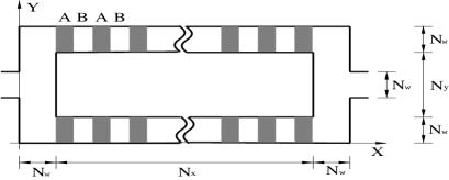
In this letter we propose an improved design of the spin filter in the Aharonov-Bohm (AB) ring structure,ab an AB frame, coupled symmetrically to two leads to further increase the SP (by one order of magnitude) and the energy intervals (channels) for the SP by the additional degree of freedom, ie. the AB flux. A schematic of the spin filter is shown in Fig. 1. A periodic spin dependent modulation with Zeeman-like form is applied symmetrically along both arms of the microstructure. Here if locates at the gray areas (A layers), and 0 otherwise. is for spin-up and -down electrons respectively. denotes a spin-independent parameter for the strength of the potential. This modulation can be realized by sticking magnetic strips on top of the sample or using magnetic semiconductor as the A layer. For , spin-up and -down electrons experience different potentials: the spin-up electrons coherently transport under the modulation of the “transparent” barriers on the arms while the spin-down ones do under the modulation of wells. The AB flux through the AB frame is introduced by a homogeneous magnetic field . For the sake of simplicity for the experimental realization, we assume this magnetic field is applied not only inside the frame, but also on the arms.
We describe the AB frame by a tight-binding Hamiltonian with the nearest-neighbour approximation:
| (1) | |||||
in which and denote the coordinates along the - and -axis respectively. () when locates at the gray (blank) areas of the frame, denotes the on-site energy with . is the hopping energy with and standing for the effective mass and the “lattice” constant respectively. With the vector potential in the Landau gauge, ie., , the hopping energy between [ and is given by .
The spin dependent conductance is calculated using the Landauer-BüttikerBu formula with the help of the Green function method.Da The two-terminal spin-resolved conductance is given by with () representing the self-energy function for the isolated ideal leads.Da We choose the perfect ideal ohmic contact between the leads and the semiconductor. and are the retarded and advanced Green functions for the conductor, but with the effect of the leads included. The trace is performed over the spatial degrees of freedom along the -axis. The spin dependent current within an energy window is given by .
We perform a numerical calculation for an AB frame with fixed arm width . A hard wall potential is applied in this transverse direction which makes the lowest energy of the th subband (mode) be . The total length and width of frame are and respectively with Å throughout the computation. The length of A layer is taken to be the same as that of B layer with . We take the Zeeman splitting energy . Unless otherwise specified, with denoting the area of the AB frame and standing for the quantum unit of flux. It is noted that .
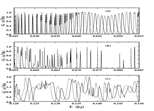
In Fig. 2 (a) and (b), the conductance is plotted as a function of the Fermi energy of the leads, with limited to the first subband. It is seen from the figure that for the AB ring structure with periodic magnetic modulations, due to the interference many energy windows are opened which give large SP, in contrast to the quantum wire where only one energy window is opened for large SP.wu The largest spin current density can be obtained from the energy window with nA for spin-up current and from the window with nA for spin-down current. A zero conductance of spin-up electron near corresponds to the energy gap due to the modulations predicted in 1D case, with the wave length of .wu A spin-independent gap between to origins from the interference effect of the four rectangular bends of the AB frame. By reshaping these four bends, we obtain the shift of this gap. Larger spin-current density can be obtained with multi-mode transport. In Fig. 2(c) we plot the conductance versus the energy in the regime of the second subband and therefore two modes participate the carrier transport. By choosing the energy window , one gets the spin current density nA.
In order to further elucidate above features of the conductance, we simplify the AB frame by taking . Therefore one can solve the problem analytically with the approach developed by Xiong.xiong The Hamiltonian, including the leads can now be simplified as
| (2) | |||||
where , 2 denotes two arms and stands for the index of sites on each arm. () labels the site of left (right) lead. Site index increases from the left to the right and two junctions between the leads and the arms are defined as the end of the leads denoted by and . We take the one-dimensional (1D) AB frame as the outer edge of the 2D structure in Fig. 1. Similar to the 2D problem, () when locates at A layer (otherwise). We take where is the lowest energy of the first subband and denote with being the energy of the incident electron. The wave-function can be expressed asxiong , with the coefficients , and being determined from the Schrödinger equation . By assuming a plane wave with unity amplitude and spin injected from the left lead, one has and with and standing for the reflection and transmission amplitudes and being the wave-vector satisfying . The transmission coefficient is therefore given as
| (3) |
in which with and with . and .
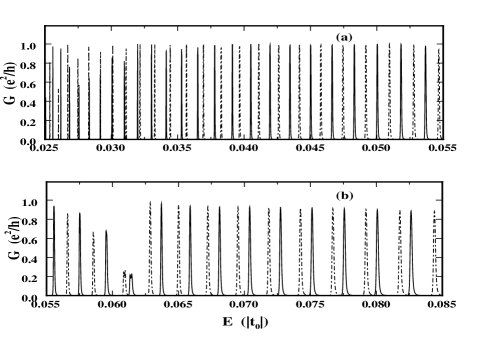
We apply the same magnetic field (and therefore the AB flux) and use the same parameters as in the 2D case. The spin-dependent conductances calculated from Eq. (3) are plotted in Fig. 3 and exhibit similar behavior as the 2D case in Fig. 2, including the band gap due to the magnetic modulation near . However, the peaks of 1D structure is much narrower and the gap caused by the four rectangular bends in Fig. 2 disappears as the bends do not exist in the 1D problem.
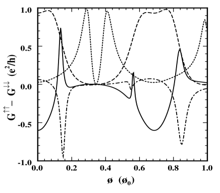
Finally we consider the effect of AB flux. In Fig. 4, the difference of the conductances of spin-up and -down electrons of the 2D AB frame is plotted as a function of the flux for four typical enegeies: (solid curve), (dotted curve), (dashed curve) and (chain curve). One finds efficient modulation due to the AB flux. Moreover, as the magnetic field is applied also on the arms of the AB frame, it is seen from the figure that the period is now roughly about , in contrast to for the case when the flux is confined inside the frame.
In summary, we have proposed a scheme for spin filter by studying the coherent transport through an AB-ring structure with lateral magnetic modulation. Large SP is predicted and is shown to be accessible with many energy intervals. The magnetic modulation can be realized by sticking the magnetic strips on top of the sample or using magnetic semiconductor as A layers.
One of the authors (MWW) was supported by the “100 Person Project” of Chinese Academy of Sciences and Natural Science Foundation of China under Grant Nos. 9030312 and 10247002. He would like to thank S. J. Xiong for valuable discussions.
References
- (1) G.A. Prinz, Phys. Today 48, 58 (1995); Science 282, 1660 (1998).
- (2) D. Loss and D. P. DiVincenzo, Phys. Rev. A 57, 120 (1998).
- (3) Semiconductor Spintronics and Quantum Computation, eds. D. D. Awschalom, D. Loss, and N. Samarth, Springer, Berlin, 2002.
- (4) G. Schmidt, D. Ferrand, L. W. Molenkamp, D. Ferrand, and L. W. Molenkamp, Phys. Rev. B 62, R4790 (2000).
- (5) M.J. Gilbert and J.P. Bird, Appl. Phys. Lett. 77, 1050 (2000); G. Papp and F.M. Peeters, Appl. Phys. Lett. 78, 2148 (2001); J.C. Egues ,C. Gould, G. Richter, and L. W. Molenkamp, Phys. Rev. B 64, 195319 (2001); Takaaki Koga, Junsaku Nitta, Supriyo Datta, and Hideaki Takayanagi, Phys. Rev. Lett. 88, 126601 (2002); J. Fransson, E. Holmström, I. Sandalov, and O. Eriksson, Phys. Rev. B 67, 205310 (2003); X.F. Wang and P. Vasilopoulos, Appl. Phys. Lett. 80, 1400 (2002); 81, 1636 (2002).
- (6) F. Sols, M. Macucci, U. Ravaioli, and Karl Hess, Appl. Phys. Lett. 54, 350 (1989).
- (7) J. Zhou, Q. W. Shi, and M. W. Wu, Appl. Phys. Lett. 84, 365 (2004).
- (8) Y. Aharonov and D. Bohm, Phys. Rev. 115, 485 (1969); D. Frustaglia, M. Hentschel, and K. Richter, Phys. Rev. Lett. 87, 256602 (2001); M. Popp, D. Frustaglia, and K. Richter, Nanotechnology 14, 347 (2003).
- (9) M. Büttiker, Phys. Rev. Lett. 57, 1761 (1986).
- (10) S. Datta, Electronic Transport in Mesoscopic Systems (Cambridge University Press, New York, 1995).
- (11) Shi-Jie Xiong and Ye Xiong, Phys. Rev. Lett. 83, 1407 (1999); Shi-Jie Xiong, Phys. Lett. A 319, 198 (2003).