Electronic transport through electron-doped Metal-Phthalocyanine Materials
Abstract
We report an insulator-metal-insulator transition in films of five metal phthalocyanines (MPc) doped with alkali atoms. Electrical conduction measurements demonstrate that increasing the alkali concentration results in the formation of a metallic state for all systems. Upon further doping, the films reenter the insulating state. Structural and Raman spectroscopy studies reveal the formation of new crystalline phases upon doping and are consistent with the phenomena originating from charge transfer between the intercalated alkali atoms and MPc, in a similar fashion to what has been so far observed only in C60. Due to the presence of a molecular spin, large exchange energy, and a two-fold orbital degeneracy in MPc, our findings are of interest in the study of controllable magnetism in molecular materials and in the investigation of new, recently predicted electronic phases.
Metal phthalocyanines (MPc’s) form a large class of molecules consisting of a stable -conjugated macrocyclic ligand bonded to a central metallic atom. They are very well known for their electronic properties, which are both of applied and fundamental interest MPcbook . In their pure form, MPc materials behave as semiconductors. Electrical conduction can be induced through doping, usually by oxidizing the ligands and creating an open shell, which results in the introduction of holes in the materials MPcreview1 ; MPcreview2 . Depending on the specific MPc molecule and the degree of oxidation, a rich variety of molecular conductors have been developed in this way. Surprisingly, in spite of the rich behavior of hole-doped MPc compounds and even though it has been shown that multiple reduction processes enable a large accumulation of electrons on different orbitals of many MPc’s Clack ; Taube , the conducting, electronic and magnetic properties of electron-doped MPc materials have remained so far vastly unexplored.
In this paper we demonstrate experimentally that it is possible to induce metallic conduction in electron-doped MPc materials and control their electronic properties, through intercalation with alkali atoms. We will first discuss the transport properties of five different compounds - CuPc, NiPc, CoPc, FePc, and MnPc - that we have investigated as a function of potassium concentration and temperature. For all these systems, insulating in the pristine state, we found that the electrical conductivity can be increased to a value in excess of =100 Scm-1 upon potassium intercalation. In this state, the conductivity of all compounds remains high at cryogenic temperatures, indicating the occurrence of metallic behavior. Increasing further the potassium concentration brings all MPc’s back into an insulating state. We will then focus on one of these molecular systems, CuPc, to address the electronic and structural properties of this compound in more detail. We discuss scanning tunnelling spectroscopy experiments that show the presence of a finite density of states in the metallic state and of a gap in the insulating states, thus confirming at the local level the occurrence of the insulator-metal-insulator transition. We also present structural investigations demonstrating the formation of intercalated phases and Raman spectroscopy measurements, which provide an independent microscopic demonstration of charge transfer between K and MPc.
Many aspects of our results bear a clear resemblance to the behavior of C60 (or, more in general, the fullerides), the only other molecular system in which a metallic temperature dependence of the conductivity induced by alkali doping has been measured in the past Haddon ; Hebard1 . As opposed to C60, MPc’s enable the tuning of many relevant parameters, such as the degeneracy of the low-energy molecular levels, the spin in the molecular ground state, the shape of the molecular orbitals orbitals and facile chemical tuning. In view of the well-established and rich electronic behavior of hole-doped MPc’s MPcreview1 ; MPcreview2 and of alkali-doped fullerides Forro ; Hebard2 ; Takenobu , we expect that controlling these molecular parameters will lead to the emergence of a rich physical phenomenology. For instance, the ability to tune the molecular spin and the large values of the exchange energy in MPc’s open the possibility to control magnetic phenomena, known to occur in different MPc compounds Magn1 ; Magn2 ; Magn3 . In addition, the two-fold degeneracy of the relevant orbitals of many MPc’s has led to the prediction of new electronic phases around half-filling Tosatti . The overall picture emerging from our experiments, together with these considerations, clearly indicates the richness of alkali-doped metal phthalocyanines as a model class of compounds for the controlled investigation of electron-doped molecular solids.
The investigation of the transport properties of alkali-doped MPc’s has been performed on thin films, thermally evaporated on the surface of a silicon-on-insulator (SOI) substrate. Film deposition, doping, scanning probe characterization, and transport measurements have been carried out in-situ in a single ultra-high vacuum (UHV) system. Figure 1 shows the conductance of films of the different MPc’s as a function of doping concentration.
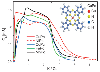
For all the materials, the conductance first increases with potassium concentration up to a high value that is comparable for the different molecules, it remains high in a broad range of concentrations, and it eventually decreases to the level observed for the pristine material. The high conductivity state (optimally doped state) occurs in a broad interval up to approximately three potassium atoms per molecule, corresponding to a much higher carrier density than what is typically achieved in holed-doped MPc compounds MPcreview1 ; MPcreview2 . From the value of the maximum conductance we find that for all MPc’s the highest electron mobility is close to 1 cm2/Vs, comparable to that of C60 Forro . We established the high reproducibility of this behavior by growing, doping, and measuring over 200 films. In the course of these experiments we also observed experimentally robust differences in the doping dependence of the conductance for the different MPc’s (visible in Fig. 1). These differences are interesting in that they systematically correlate to the known properties of the MPc molecular orbitals and suggest that electrons can be added to orbitals that are centered either on the ligands or on the metal atoms, depending on the specific molecule. This behavior MPc-JACS expected on the basis of existing calculations for individual MPc molecules orbitals , is different from the case of hole-doped MPc compounds, in which the holes typically occupy the ligand orbitals only.
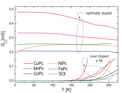
To investigate the nature of electrical conduction in the MPc films, we have measured the temperature dependence of the conductivity for different doping levels (Fig. 2). For the undoped films, the conductance is decreasing with decreasing temperature as expected for insulating materials. When the films are doped into the highly conductive state, for all MPc’s the conductance remains high when lowering the temperature and the films are conducting down to low temperature, demonstrating the occurrence of metallic conduction. In the overdoped state the conductance again decreases very rapidly with decreasing temperature. This evolution of the temperature dependence of the conductance unambiguously reveals that an insulator-metal-insulator transition occurs in all five MPc’s upon doping with K.
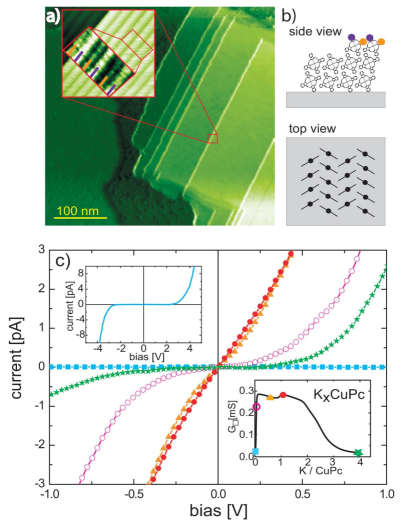
In order to investigate the microscopic nature of the insulator-metal-insulator transition, we have performed scanning tunnelling spectroscopy on highly ordered CuPc films, a few monolayer thick, before and after K-doping. To make this possible, films with large domains were grown on 21-reconstructed Si(001) surface. High resolution scanning tunneling microscopy (STM) images of our films are shown in Fig.3a. The film morphology consists of a fully closed first monolayer and highly ordered islands typical of the Stranski-Krastanov growth mode. Zooming in on a molecular terrace (first inset in Fig.3a) reveals that the molecules grow in ordered columns which lie flat on the Si(001) surface aip ; growth1 as shown in the schematic diagram of the molecular structure of Fig.3b. Further zooming in on the molecular columns (second inset in Fig.3a) shows that each column exhibit features corresponding to the uppermost phenyl rings of a CuPc molecule.
STS measurements on thin, undoped CuPc films shows a very large apparent gap of several volts (Fig.3, upper inset). This is because undoped films are highly resistive and a considerable fraction of the voltage applied between the substrate and the STM tip drops across the CuPc layers (i.e., the gap in the I-V curves is not the HOMO-LUMO gap of CuPc). Upon doping, the magnitude of the gap rapidly decreases (Fig.3). When the doping level corresponds to a state of high conductivity, the tunneling gap vanishes and a finite slope is observed in the tunneling curves around zero bias voltage, which indicates a finite density of states in the doped film. Upon further doping of the films, a large gap in the tunneling curve is observed again. Therefore, the STS data fully support the conclusion drawn from the temperature dependence of the conductance: at low and high doping level the CuPc film is insulating, in the intermediate region it is metallic (see Fig.2). Other MPc’s on which we have performed similar, but less systematic, STS experiments show a similar behavior.
The behavior of K-doped CuPc films suggests a progressive filling
of one or more molecular orbitals with electrons transferred from
potassium into the molecular film. The complete filling is mainly
supported by the fact that after reaching the metallic state, the
conductance of the film decreases to the level of the pristine
material. Note that this observation excludes the possibility that
the observed conduction is an experimental artifact, such as, for
instance, the formation of a potassium surface layer. Further, we
have observed that the doping process is reversible: overdoped
K-CuPc films can be de-doped by exposure to oxygen, which removes
electrons from the film by oxidizing K. This excludes the
occurrence of irreversible chemical reactions between K and the
MPc’s.
With the exception of the fullerenes, this is the first time that
a molecular system has been shown to exhibit an
insulator-metal-insulator transition upon doping with alkali
atoms. Previous work on different molecules had shown that charge
transfer from the alkali atoms does occur and that, in certain
cases, a finite density of states can be induced
PES-KCuPc ; PES1 ; PES2 ; pentacene ; Iwasaki . However, a
low-temperature metallic conduction had never been observed in
these systems, which typically exhibited thermally activated
decrease of conductivity with lowering temperature Iwasaki .
Interestingly, such a behavior is what we observe when we measure
CuPc films grown on SiO2 substrates. The difference between
films grown on Si and on SiO2 originates from structural
disorder, which for films grown on SiO2 has been proven to be
much larger than for films grown on Si growth1 ; growth2 . The
large influence of disorder on transport properties is consistent
with our observation that the highest carrier mobility in MPc
films deposited on SiO2 is only
cm2/Vs, i.e. times smaller than the mobility
found in films deposited on a Si surface.
Having established the similarity of the phenomenology upon alkali intercalation of MPc’s and C60 thin films, we then started to explore the structural properties of the materials. In particular, whereas in pristine C60, there is well-defined interstitial space to accommodate the alkali ions in the parent crystalline structure, it is not immediately obvious how this might be achieved in pristine MPc’s without major structural modifications. Since it is technically impossible for us to undertake in-situ X-ray diffraction (XRD) and Raman measurements in the same UHV system used for the investigation of transport properties, we have performed these experiments on polycrystalline powdered samples.
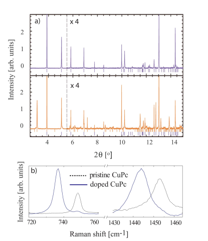
Figure 4a shows the high-resolution synchrotron XRD powder patterns of pristine (-phase betaCuPc ) and K-doped CuPc. The measured diffraction profile of the material after K-doping comprises peaks arising from a residual fraction of the pristine compound together with additional reflections due to the formation of a new crystalline phase. The latter can be indexed with a primitive monoclinic unit cell with lattice constants a = 25.2311(4) Å, b = 4.4049(3) Å, c = 21.6272(5) Å, and = 93.924(4)o and an expanded unit cell volume relative to the pristine copper phthalocyanine by 12 Å3/CuPc unit. These findings demonstrate the existence of at least one stable intercalated phase in the potassium-CuPc phase field. Work is in progress towards complete structural determination and to search for additional intercalated phases at different doping levels.
We have also performed Raman spectroscopy studies on the same samples used for the structural characterization and compared the results for the doped and pristine material (see Fig.4). The undoped sample shows features, assigned to the C-N and C-H bonds of the CuPc molecule in agreement with previous studies betaCuPc . Many of these lines are also found unshifted in the doped sample, consistent with the presence of pristine material. However, as shown in Fig. 4, the doped material also exhibits new vibrational lines shifted towards lower wavenumbers. The values found for the doping-induced Raman shifts range from 7.6 cm-1 to 18.6 cm-1 for different lines. This shift confirms the occurrence of charge transfer from the potassium atoms to the CuPc molecules.
In conclusion, we have performed a systematic investigation of the
electronic and structural properties of electron-doped metal
phthalocyanine compounds, through the intercalation of potassium
atoms. As compared to known hole-doped materials based on the same
molecules, electron doping gives access to a broader range of
electron density. This has enabled us to reveal an
insulator-metal-insulator transition in the conductivity of the
molecular materials with increasing doping, similar to what had
been so far only observed in C60. The combination of the
large density range accessible by electron doping and the various
molecular properties of metal phthalocyanines, i.e.,
controllable spin, two-fold orbital degeneracy, orbital symmetry,
and large exchange energy, make alkali-doped metal phthalocyanine
compounds unique for the study of new electronic phenomena,
ranging from controllable magnetism to the occurrence of novel,
recently predicted, electronic phases Tosatti .
We thank J. van den Brink and E. Tosatti for useful discussions,
Y. Taguchi and T. Miyake for experimental help, A.N. Fitch for
help with the diffraction experiments, the ESRF for provision of
beamtime and are grateful to AMOLF for the RBS analysis of our
samples. This work was financially supported by the stichting FOM,
the Netherlands Organization for Scientific Research (MFC), the
Royal Dutch Academy of Sciences KNAW (SR), the NWO
Vernieuwingsimpuls 2000 program (AFM), the Royal Society (Dorothy
Hodgkin Research Fellowship to SM) and the Daiwa Foundation
(KP).
Experimental
Preparation of alkali-doped Metal-Phthalocyanines thin
films : All the steps of our investigations have been carried out
in the UHV system with a base pressure mbar. This prevents the occurrence of degradation of
the doped films over a period of days. Prior to the film
deposition, as-purchased compounds were heated in UHV at a
temperature just below their sublimation temperature for several
days, to remove contaminants. The films were thermally evaporated
from a Knudsen cell onto a hydrogen (wet) passivated silicon (001)
surface of a silicon-on-insulator (SOI) wafer, consisting of a top
2m silicon layer electrically insulated from the Si substrate
by 1m-thick SiO2 buried layer. The use of SOI as
substrate permits to grow high-quality MPc films, which is only
possible on a crystalline Si surface growth1 , while
avoiding a large parallel electrical conduction through the entire
Si substrate. The typical film thickness was 20 nm. For the
scanning probe experiments, films with large domains, a few
monolayer thick, were grown at 500K on a 21-reconstructed
Si(001) surface. Alkali doping was achieved by exposing the film
to a constant flux of K atoms generated by a current-heated getter
source. In order to determine the potassium concentration in the
film, we have performed an elemental analysis for several doping
levels using ex-situ RBS for CuPc. We have then used the K-CuPc
data to scale the concentration of the other molecular films as a
function of potassium exposure time and film thickness (note that
this method is affected by a relatively large uncertainty in
K/MPc, which we estimate to be approximately of the order of one
at a high doping level).
Preparation of polycrystalline powdered samples: Potassium-doped CuPc was synthesized in bulk form by a direct reaction of K vapor and CuPc powder in sealed glass tubes, heated at 300oC for three weeks. Prior to this procedure, as-purchased CuPc powder was purified in a thermal gradient by vacuum sublimation. All sample manipulations were undertaken in an Ar-atmosphere glove box with an oxygen concentration 1 ppm. After the reaction, the as-synthesized material was introduced into glass capillaries and sealed under Ar gas. Synchrotron X-ray powder diffraction patterns of pristine and K-doped CuPc were recorded on the ID31 beamline at the European Synchrotron Radiation Facility (ESRF, Grenoble, France) at ambient temperature and = 0.85001 .
References
- (1) N. B. McKeon, Phthalocyanine materials, Cambridge University Press, (New York 1998).
- (2) T. Inabe, and H. Tajima, Chem. Rev. 104, 5503 (2004).
- (3) T. J. Marks, Angew. Chem. 29, 857 (1990).
- (4) D. W. Clack, and J. R. Yandle, Inorg. Chem. 11, 1738 (1975).
- (5) R. Taube, and H. Drevs, Angew. Chem. Internat. Edit. 6, 358 (1967).
- (6) R. C. Haddon, A. F. Hebard, M. J. Rosseinsky, D. W. Murphy, S. J. Duclos, K. B. Lyons, B. Miller, J. M. Rosamilia, R. M. Fleming, A. R. Kortan, S. H. Glarum, A. V. Makhija, A. J. Muller, R. H. Eick, S. M. Zahurak, R. Tycko, G. Dabbagh, and F. A. Thiel, Nature 350, 320 (1991).
- (7) G. P. Kochanski, A. F. Hebard, R. C. Haddon, and A. T. Fiory, Science, 255, 184 (1992).
- (8) M. S. Liao, and S. Scheiner, J. Chem. Phys. 114, 9780 (2001).
- (9) L. Forro, and L. Mihaly, Rep. Prog. Phys. 64, 649 (2001).
- (10) A. F. Hebard, M. J. Rosseinsky, R. C. Haddon, D. W. Murphy, S. H. Glarum, T. T. M. Plastra, A. P. Ramirez, and A. R. Kortan, Nature 350, 600 (1991).
- (11) T. Takenobu, T. Muro, Y. Iwasa, and T. Mitani, Phys. Rev. Lett. 85, 381 (2000).
- (12) M. Evangelisti, J. Bartolome, L. J. De Jongh, and G. Filoti, Phys. Rev. B 66, 144410 (2002).
- (13) K. Awaga, and Y. Maruyama, Phys. Rev. B 44, 2589 (1991).
- (14) M. Y. Ogawa, S. M. Palmer, and K. Liou, Phys. Rev. B 39, 10682 (1989).
- (15) E. Tosatti, M. Fabrizio, J. Tobik, and G.E. Santoro Phys. Rev. Lett. 93, 117002 (2004).
- (16) M. Nakamura, and H. Tokumoto, Surf. Sci. 398, 143 (1998).
- (17) M. F. Craciun, S. Rogge, and A. F. Morpurgo, J. Am. Chem. Soc. 127, 12210 (2005).
- (18) M. F. Craciun, S. Rogge, D. A. Wismeijer, M. J. L. den Boer, T. M. Klapwijk, and A. F. Morpurgo, AIP Conf. Proc. 696, 489 (2003).
- (19) T. Schwieger, M. Knupfer, W. Gao, and A. Kahn, Appl. Phys. Lett. 83, 500 (2003).
- (20) L. Yan, N. J. Watkins, S. Zorba, Y. Gao, and C. W. Tang, Appl. Phys. Lett. 79, 4148 (2001).
- (21) T. Schwieger, H. Peisert, M. S. Golden, M. Knupfer, and J. Fink, Phys. Rev. B 66, 155207 (2002).
- (22) T. Minakata, M. Ozaki, and H. Imai, J. Appl. Phys. 74, 1079 (1993).
- (23) K. Iwasaki, K. Umishita, M. Sakata, and S. Hino, Synth. Metals 121, 1395 (2001).
- (24) J. Le Moigne, and R. Even, J. Chem. Phys. 83, 6472 (1985).
- (25) M. Nakamura, Y. Morita, Y. Mori, A. Ishitani, and H. Tokumoto, J. Vac. Sci. Technol. B 14, 1109 (1996).
- (26) R. Prabakaran, R. Kesavamoorthy, G. L. N. Reddy, F. P. Xavier, Phys. Stat. Sol. B 229, 1175 (2002).