Reduction of the Three Dimensional Schrödinger Equation for Multilayered Films
Abstract
In this paper we present a method for reducing the three dimensional Schrödinger equation to study confined metallic states, such as quantum well states, in a multilayer film geometry. While discussing some approximations that are employed when dealing with the three dimensionality of the problem, we derive a one dimensional equation suitable for studying such states using an envelope function approach. Some applications to the Cu/Co multilayer system with regard to spin tunneling/rotations and angle resolved photoemission experiments are discussed.
pacs:
72.25.Mk,73.21.FgI Introduction
There has been much recent interest in magnetoelectronic devices due to their potential applications as miniaturized computer memory components and high speed analog devices one ; two . The ability to synthesize systems with artificial structures has grown remarkably over the past decade. For example, it has been shown recently that molecular beam epitaxy techniques allow for the growth of independent ferromagnetic layers on a semiconducting substrate, in cases such as Fe on InAs(100) two and MnGa on GaAs(100) four . The search for new device materials and making optimum use of such new devices will greatly benefit from an accurate understanding of the underlying quantum mechanical processes involved in electron transport as the dimensions of the device approach the wavelength of transmitting electrons. Recent experimental studies of spin dependent, hot electron transmission such as those described in Ref. filipe, and resonant tunneling through two discrete states (Ref. vaart, ), have raised a number of interesting issues related to the ferromagnetic and insulating materials used, the nature of the electronic states that are involved in transmission and enhancements in spin filtering effects. Apart from the first principles based attempts which can be quite tedious, most theoretical studies of these spin dependent effects have used free electron band structures and other simplifications in the metallic as well as in the insulating regions. Our work, though motivated by free electron approaches such as those introduced by Slonczewski sol1 , is an attempt to bring out a more realistic lateral dependence of the electronic states under consideration.
This paper is organized as follows. First, starting from the three dimensional Schrödinger equation, we proceed to derive an envelope function approach suitable for multilayered films. This procedure will go beyond the free electron methods that have been commonly used in the past, making use of more realistic wave functions, but avoiding a full pledged ab-initio calculation when studying such systems. We introduce an approach which incorporates the two dimensional Bloch wave vector and show that the associated parallel band structure characteristic of the material being used, plays a major role in perpendicular transmission.
Second, We will study spin tunneling and rotation effects (to be defined later) in a multilayer system with two ferromagnetic layers separated by a nonmagnetic metal such as Co/Cu/Co. We will also address some issues related to angle resolved photoemission and inverse photoemission experiments focused on confined states in metallic multilayers. Although there have been attempts to explain such spectra using a Phase Analysis Model (PAM) with some success curti , a better understanding of the multilayering, tunneling, spin rotation effects etc. is necessary, for example, to go beyond simple situations and study more complicated heterostructures of different sizes and shapes. For such systems, quantum mechanical calculations of spin-dependent transmission using a simple free-electron model have already been preformed six ; ten . However, there is a growing need for more realistic, yet simple enough calculations in order to understand new and small structures that are being synthesized today.
II Model and Approximations
There have been some recent attempts to evaluate the effects of the two dimensional (planar), metallic periodic structures on the confined states in various devices using simplified models butler . Some of these have focused on a Fourier space description of the one particle Schrödinger wave function. We will be examining some of the assumptions made in these Fourier as well as real space models about the confined states, the effects of the planar regions on them and the importance of spin asymmetry on the spin filtering process.
Our model consists of multilayered slabs of different materials sandwiched together to form a device. For example, the device may contain several layers of Cu sandwiched between two ferromagnetic slabs of Co as in Co/Cu/Co. We will choose the direction to be perpendicular to these slabs and the to be parallel planes consisting of slabs. These can also be labeled longitudinal and transverse directions respectively. There are several simplifications that are usually made in attempts to calculate properties of such structures. When approximations are made to the wave function near an interface, it is a common practice to separate the transverse dependence and the longitudinal dependence (see Ref. butler, ). Let us carefully consider the conditions on the one particle potential and the tunneling states that lead to such a description of the problem at hand. An arbitrary eigenstate here can be expressed in the (planar) Bloch form as
| (1) |
and the one particle potential can be expressed as
| (2) |
to elucidate the periodic nature of the potential and the Bloch-like form of the wave function in the planar (i.e. parallel) direction. Here refers to a planar reciprocal lattice vector, while .
It is possible to analyze the effects of the planar states on the perpendicular behavior in several different ways. First, using the Fourier coefficients defined above, the complete one particle solution may be expressed as,
| (3) |
Note that unless the (parallel and z direction) potential coefficients are weak compared to the relevant energy scale of the problem, the above equation couples the Fourier coefficients of the wave function through the potential coefficients and hence does not necessarily yield exponentially decaying solutions in the perpendicular (z) direction for the wave function even if the energy satisfies the condition,
| (4) |
for all values of .
Consider the wave function as defined in Eq. (1). An assumption that is usually made butler when looking for such solutions is the following ”separability” condition:
| (5) |
The assumption of the wave function separating into planar () and perpendicular () parts is equivalent to having , where Fourier coefficient has no dependence. These ideas can be expressed in terms of the one particle potential and its Fourier expansion given by Eq. (2). It is clear that if this potential satisfies the (additivity) condition, with no coupling between the planar and perpendicular dependencies, then the above separation of variables in the wave function can be justified. In such situations, the Hamiltonian H also becomes additive as and a simple quantum well equation,
| (6) |
can be obtained for the .
However, we argue that the above assumptions are too restrictive when one is dealing with states that have , or character in local orbital angular momentum. The coupling of the three directions in the wave functions have to be dealt with more rigor, since such atomic wave functions are unlikely to satisfy the separability condition expressed in Eq. (5). Significant corrections will be necessary if the separability condition is used as a starting point for better calculations. Hence we have sought a different starting point for carrying out the reduction of the three dimensional Schrödinger equation. The envelope function approach discussed below provides an ideal and formal platform for handling the situation at hand.
III Envelope Functions and the Full Problem
With the advent of methods related to semiconductor quantum wells, the simplistic theory surrounding them has been so successful that sometimes it is easy to undermine its connections to the well understood regime of weak perturbations in bulk crystals. However, since the potentials employed in quantum wells are strongly perturbed at various boundaries, some formal justification seems necessary in order to use simple quantum well equations for multilayer systems. In fact, some applications of quantum well based techniques to semiconductor heterostructures have been justified using an envelope function approach burt .
In principle, the relevant many particle Hamiltonian in all the different regions of the heterojunction carries all the necessary (interaction) information. When combined with the proper boundary conditions, its appropriate eigenstates can be used to describe, for example, tunneling in such a device. However, this problem is highly nontrivial and various approximations are sought in order to simplify it. First principles methods, such as those based on the density functional theory, can be utilized for this purpose but less complicated approaches that can reduce the computational burden are quite attractive. The envelope function method introduced by Bastard nine is one such approach. Here the real space equations satisfied by the envelope functions were equivalent to the method of Kane kane with the band edges allowed to be functions of position. For heterojunctions with planar metallic regions, the applications of such ideas can be clarified and presented in a relatively straightforward way starting from the nonrelativistic three-dimensional Schrödinger equation:
| (7) |
As is commonly done for (nonrelativistic) itinerant systems, the spin dependence in the Hamiltonian has been absorbed into a spin dependent potential , and the two equations representing the up and down spins can be solved separately. Hence, from now on, we will drop the spin index and focus on the reduction of a single, one particle Schrödinger equation. In the parallel direction, the metallic as well as insulating regions are assumed to have perfect, two dimensional crystalline order, giving rise to extended electronic states with well defined parallel Bloch momenta . We also assume perfect (parallel) lattice vector matches at various interfaces.
An important point to note here is that in these problems that involve heterojunctions, there are (at least) two relevant length scales; namely the interatomic length scale and the scale associated with the (confining) structures. The envelope function may vary on the latter length scale or on some combination of the two, which is to be determined later. Based on this argument, one can expect a nontrivial envelope function, when it exists, to modify the rapidly varying atomic wave functions. We regard this as our starting point and express the full problem (ignoring the spin dependence) as:
| (8) |
The function can be thought of as a wave function with rapid variations on the atomic scale that has the two dimensional Bloch character, while is an envelope function as described above. An important point to note here is that we do not make an assumption on separability as in Eq. (5). The existence of a nontrivial envelope function, as identified by the above equation, will be used as a prerqusite for the existence of quantum well or other confined states. Our search is for envelope functions, as defined above, that are likely to arise due to the confining structures. One can question the validity of such an expression, and similar forms have been suggested burt such as an expansion using products of Bloch states and envelope functions. Here, we use the above form and associate an eigenvalue with the function through the following eigenvalue problem.
| (9) |
We note that this is similar to how two dimensional band structure is calculated for thin films. Although for simplicity, we do not address interface roughness and other similar issues in this paper, the potential in Eq. (8) can be modified to include such effects with appropriate changes in the boundary conditions (and a z dependent potential in Eq. (11)). With the above definition of (subband energy), the full Schrödinger equation can be used to obtain a differential equation for the envelope function in the following manner.
| (10) |
The second term on the left hand side of the above equation contains a product of first order derivatives and describes some coupling of the lateral (i.e. planar) and longitudinal (i.e. perpendicular) coordinates, in addition to any coupling that is already contained in . This coupling term can be simplified using averages of over the planar coordinates. In general, this will result in a dependent term and a second order differential equation for as,
| (11) |
with
| (12) |
The double integral over the planar coordinates has to be carried out over a suitable 2 dimensional unit cell. This is a mathematically rigorous result, based solely on the assumptions stated previously, and the theory at this level cannot and should not distinguish between metals, semiconductors or insulators.
Now we can look for possible simplifications to Eq. (11) by monitoring the properties of . Note that if the Bloch function has an oscillatory dependence, then will be purely imaginary. However, the imaginary part of () is directly related to the averaged flux, along the direction. Hence, we can make use of (steady state) flux conservation which leads to ; i.e. the conservation of flux implies that has to be independent of . When has a non negligible real part, we cannot make use of the above argument, and the type of confined states that we are searching for (through Eq. (14) ), will not exist. However, note that even for this situation, we have achieved the reduction of the 3 dimensional Schrödinger equation to a one dimensional one. Now setting (z-independent), the substitution
| (13) |
can be used to eliminate the first order derivative leading to a familiar equation, similar to Eq. (6). The function appearing here has a different interpretation, as a part of an envelope function, and the boundary conditions in the quantum well problem should be applied to the envelope function or . Note that that if and its derivative are continuous across various boundaries along the direction, then similar properties can be established for .
| (14) |
The above equation illustrates several important points that are often overlooked or misinterpreted in simplistic quantum well and free electron approaches. As observed in Ref. (butler, ), a possible reduction in tunneling rates can be expected due to the lateral variation of the wave function. Although our method is somewhat different, note that Eq. (4) of Ref. (butler, ) has a averaged term similar to in our discussion, which affects, for example, decay rates associated with functions differently. The subband structure, i.e. , in the multilayers affect the confined eigenstates and eigenvalues. The envelope functions are also affected by the averages of the parallel Bloch functions through . For each ‘confined energy level’ with energy , there exists a continuous subband of states that share the same perpendicular wave function but differ in parallel Bloch momentum , and . Note that can depend on the thickness of a given multilayer film and carries information not only about the planar structures, but also about the longitudinal coupling, following our definition through Eq. (9). Finally, the energy of a given electron in such a quantum mechanical state depends on all of the above.
IV Applications - Confined States in Metallic Multilayers
We are now ready to apply our model to test devices. The first device consists of several layers of (nonmagnetic) Cu, sandwiched between two slabs of (ferromagnetic) Co (i.e. Co/Cu/Co) which will be used to discuss spin transmission/rotation effects. For an incident electron of energy , we obtain the following electronic perpendicular momenta,
| (15) | |||
| (16) |
where () is the perpendicular wave vector for majority (minority) electrons in the ferromagnetic, metallic regions where the lateral effects have been taken in to account using the ideas developed in the previous sections. Here is the spin splitting in the two dimensional bands assumed to be k|| independent.
In this device, we can rotate the magnetization of the right (R) ferromagnet by an angle with respect to the magnetization of the left (L) ferromagnet. The spin rotation is introduced at the boundary inside the spacer (Cu) layer for simplicity. For this device, solutions to Eq. (14) in various spatial regions (L and R, subdivided into ) take the form,
| (21) | |||||
| (26) | |||||
| (31) | |||||
| (36) |
Finally, we impose the boundary conditions at (where is the thickness of the center slab) and at for spin rotations.
| (41) | |||||
| (46) | |||||
| (51) |
and identically for the first derivative. The matrix is the spinor transformation, where is tied to the spin rotation effects as discussed below. We can then fully determine the transmission coefficients utilizing numerical techniques.
IV.1 Spin Transmission and Rotations
An interesting application of the above ideas has to do with ballistic transport and spin rotation effects. When polarized electrons are transmitted from one region to another with a different polarization axis, they experience a spin-torque and a transfer of angular momentum to the new medium sol2 . These ideas have now been demonstrated experimentally, for example, through the phenomenon of giant magnetoresistance where large current densities flowing perpendicular to the films have been observed in reversals of magnetization myers , and spin precession web . This field is an emerging one related to ‘magnetoelectronics’ and many new experiments are expected to be conducted on spin transmission/rotation effects in magnetic multilayer systems.
We do not wish to focus on the mechanisms of spin transfer but simply use spin rotation angle as an input to our calculations and obtain the corresponding transmission coefficients in a device consisting of two magnetic films separated by a nonmagnetic one (i.e. Co/Cu/Co). Spin rotation effect is introduced, by hand, at the center of the nonmagnetic film (Cu) for simplicity as has been done previously sol1 . However, unlike in the previous studies, the underlying band structure and lateral effects have been taken into account by using the theory of confined states developed here. These band dispersions play a crucial role in determining the spin dependent transport properties. For example, when such confined states in a ferromagnetic film are located in a gap of minority spin states, the system can act as an almost perfect spin filter . The k-dependent transmission coefficients, and that were introduced in the previous section can be used through a Landauer type formula lan ,
| (52) |
to obtain the conductivity in the quantum well problem under discussion. Here we calculate transmission coefficients along using selected subbands, as defined in Eq. (53),
| (53) |
in the transmission device (Co/Cu/Co) for the following set of parameters (Fig. 1) for illustrational purposes: W(Co)= 0.07, W(Cu)= 0.06, = 0.19 (all in Rydbergs), = 13.6, a= 6.8 (all in Bohrs).
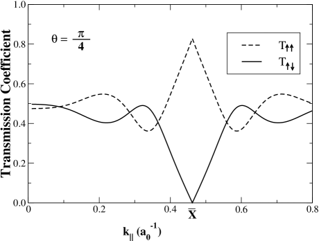
At a given (total) energy of the incoming electron, and a given relative spin orientation of the Co films, transmission coefficients have been obtained from Eqs. (36) and (51) as a function of the parallel Bloch momentum, . From this figure, it is easy to see the effects of different types of Bloch states on the tunneling. Near the zone boundary , for the given relative spin orientation , we see the device filtering out ‘minority’ spins, while at other k-points along , a mixture of both ‘majority’ and ‘minority’ spins are transmitted. This is a direct result of the upward dispersion of the selected subbands along and the spin splitting in Co, pushing the minority band closer to the given (total) energy of the electron.
IV.2 Energy Spectrum and Photoemission
Angle Resolved Photoemission (ARP) techniques have become a useful tool for studying electronic states and their (band) dispersions in structures with two dimensional (planar) Bloch symmetry. In ARP experiments photons are used to eject electrons from occupied states while in inverse ARP, photons are ejected, when the above photoemission process is reversed. Photoemission is a many body phenomenon and an evaluation of the spectral function and appropriate self-energies yield the full photoemission spectrum and peak widths. However, here we follow a simpler approach and focus on one particle energy states and the changes introduced by the multilayering. In this approach, the energy that is measured for the photoemitted electron can be associated with the full Schrödinger equation (7). Existence of an envelope function as defined in Eq. (8) and satisfying the imposed boundary conditions are necessary for confined states. The energy as defined through Eq. (9) has to do with the ordinary subband states due to the periodic potential in the planar directions. If the multilayering does not play any role for a given energy at a given , then and have to be identical when these solutions exist in Eqs. (7) and (9). In such cases, turns out to be a simple multiplicative constant and Eq. (10) is consistent with this scenario. However, when confined states exist, they may alter the usual dispersions that are observed in their absence. According to the theory developed above, confined states can be identified as states for which solutions to the differential equation (14) exist for a given energy of the electron. It is also important to realize that, for a given energy , these states may not exist for all values of along a given direction of the 2 dimensional Brillouin zone.
In general, the dispersion of the total energy of the electron , i.e. the energy of the bound electron as a function of , are found whenever confined states exist with appropriate as solutions to Eq. (14). In the present context, with boundary conditions appropriate to stationary states (determined by the film geometry), we obtain a set of discrete energies () and states for the one dimensional quantum well or barrier problem where
| (54) |
Hence, the observed energies in an ARP experiment for confined states will depend on the existence of these discrete s and the corresponding functions satisfying the relevant boundary conditions. As in simple quantum well problems, solutions of odd and even parity may sometimes be associated with and these will depend on the film geometry, interfaces and growth conditions. We plan to address these as well as effects due to film thickness (observed in Refs. curti, ; wu, ) in a future paper.
V Conclusions
Using an envelope function approach, we have reduced the three dimensional Schrödinger equation to a one dimensional one and analyzed the lateral effects of metallic multilayer films through a hypothetical subband structure that varies with the two dimensional Bloch vector. Ballistic transmission in a magnetoelectronic device consisting of Co/Cu/Co has been examined and shows a clear dependence on the Bloch vector . Energy spectrum of confined multilayer states that may be observed in angle resolved photoemission studies are discussed. Also, this method of reduction of the Schrödinger equation with appropriate modifications may be used in other confined geometries such as nanoparticles and wires.
VI Acknowledgements
The authors wish to thank Dr. B. Sinkovic for useful discussions. This work has been supported by the National Science Foundation REU program at the University of Connecticut.
References
- (1) Physics Today 48 (1995) pp.24-63.
- (2) Y.B. Xu, D.J. Freeland, E.T.M. Kernohan, W.Y. Lee, M. Tselepi, C.M. Guertler, C.A.F. Vaz, J.A.C. Bland, S.N. Holmes, N.K. Patel and D.A. Ritchie, Jour. Appl. Phys. 85, 5369 (1999).
- (3) W. van Roy, H. Akinaga, S. Miyanishi and K. Tanaka, Appl. Phys. Lett. 69, 711 (1996).
- (4) A. Filipe, H. -J. Drouhin, G. Lampel, Y. Lassailly, J. Nagle, J. Peretti, V. I. Safarov, and A. Schuhl, Phys. Rev. Lett., 80, 2425, (1998); D. J. Monsma, J. C. Lodder, T. J. A. Popma, B. Dieny, ibid, 74, 5260 (1995).
- (5) N. C. van der Vaart, S. F. Godijn, Y. V. Nazarov, C. J. P. M. Harmans, J. E. Mooij, L. W. Molenkamp, C. T. Foxon, Phys. Rev. Lett., 74, 4702 (1995).
- (6) J.C. Slonczewski, Phys. Rev. B 39, 6995 (1989).
- (7) Z. Zheng,Y. Qi, D.Y. Xing and J. Dong, Phys. Rev. B 59, 14505 (1999).
- (8) F. G. Curti, A. Danese, and R. A. Bartynski, Phys. Rev. Lett., 80, 2213 (1998).
- (9) J.E. Ortega and F.J. Himpsel, Phys. Rev. Lett. 69, 844 (1992).
- (10) F. T. Vasko and A. V. Kuznetsov in Electronic States and Optical Transitions in Semiconductor Heterostructures, Springer (1998).
- (11) J.P. Sun, G.I. Haddad, P. Mazumder and J.N. Schulman, Proc. of the IEEE, 86, (1998).
- (12) G. Bastard, Phys. Rev. B24, 5693 (1981); G. Bastard, J. A. Brum and R. Ferreira, Solid State Physics, Vol. 44, Academic Press, New York, p229 (1991).
- (13) T. Hayashi, M. Tanaka, and A. Asamitsu, Jour. Appl. Phys. 87, 4673 (2000).
- (14) M. G. Burt, J. Phys. Condens. Matt. Phys. R53 (1999); M. G. Burt, ibid, 4, 6651 (1991).
- (15) E. O. Kane, Semiconductors and Semimetals, Vol. 1, p 75, Academic Press, New York (1975).
- (16) W. H. Butler, X.-G. Zhang, and T. C. Schulthess and J. M. MacLaren, Phys. Rev. B 63, 092402 (2001).
- (17) J. C. Slonczewski, J. Magn. Magn. Mater., 159, L1 (1996); 195, L261 (1999); L. Berger, Phys. Rev. B 54, 9353 (1996).
- (18) E. B. Myers, D. C. Ralph, J. A. Katine, R. N. Louie and R. A. Buhrman, Science 285, 867 (1999).
- (19) W. Weber, S. Rieseen, and H. C. Siegmann, Science 291, 1015 (2001).
- (20) R. Landauer, Philos. Mag. 21, 863 (1970); M. Büttiker, IBM Res. Dev. 32, 317 (1988).
- (21) Y. Z. Wu, C. Y. Won, E. Rotenberg, H. W. Zhao, F. Toyoma, N. V. Smith and Z. Q. Qiu, Phys. Rev. B 66,245418 (2002).