Quantum Shot Noise Suppression in Single-Walled Carbon Nanotubes
Abstract
We study the low frequency current correlations of an individual single-walled carbon nanotube at liquid He temperature. We have distinguished two physical regimes – zero dimensional quantum dot and one dimensional quantum wire – in terms of an energy spacing from the finite tube length in both differential conductance and shot noise measurements. In a one dimensional wire regime, we observed a highly suppressed shot noise from all measured tube devices, suggesting that electron-electron interactions play an important role.
pacs:
73.23.Ad, 72.15.Nj, 73.40.Cg, 73.63.FgSingle-walled carbon nanotubes (SWNTs) have been an attractive material for over a decade due to their unique chemical, mechanical and electronic properties. They are molecular quantum wires Dekker99 , an ideal system to probe low-dimensional physics. Since SWNTs have both spin and orbital degeneracy, conductance with ideal contacts yield two times of spin-degenerate quantum unit of conductance, . Conductance measurements of SWNTs coupled to metal electrodes have demonstrated remarkable electrical transport properties: Coulomb blockade oscillation Bockrath97 , the Kondo effect Nygard00 , ballistic quantum interference Liang01 ; Kong01 , and Luttinger-liquid behavior Bockrath99 .
Noise experiments in carbon nanotubes, however, are relatively recent for two main reasons: the difficulty to fabricate nearly-ohmic contacted SWNT devices Javey03 , and a technical obstacle to achieve a high signal-to-noise ratio because of a weak excess-noise signal embedded in the prevalent background noise. Only a few groups, in fact, have reported noise of SWNTs and multi-walled nanotubes Collins00 , and shot noise measurements on an ensemble of SWNTs Rouche02 .
Shot noise refers to the non-equilibrium current fluctuations resulting from the stochastic transport of quantized charge carriers. When electron transport is governed by Poisson statistics as in the random emission of electrons from a reservoir electrode, the spectral density of the current fluctuations reaches full shot noise , where is the electron charge and is the average current. In a mesoscopic conductor, quantum shot noise occurs due to the random partitioning of electrons by a scatterer. If the noiseless incoming electrons from a Fermi-degenerate reservoir at zero temperature are scattered into the outgoing states with a transmission probability , the transmitted electrons carry partition noise . is the ratio between the spin-degenerate quantum unit of conductance and the measured DC conductance for a ballistic conductor Buttiker92 . Noise in a quantum system is quantified with the Fano factor .
Quantum shot noise has been observed with quantum point contacts (QPCs) in two-dimensional electron gas systems Liu98 ; Oliver99 . Recently proposed detection schemes for entangled electrons have uitilized the analysis of shot noise correlations Maitre00 ; Burkard00 ; Samuelsson03 . Moreover, shot noise measurements allow one to observe the effective charge of quasiparticles along fractional quantum Hall edge states Picciotto97 ; Comforti02 , yielding and . Electron-electron interactions in one-dimensional edge states result in fractionally charged carriers. This strongly correlated 1D system is modelled as a “Luttinger liquid” (LL).
A LL exhibits power-law scaled conductance ( in terms of temperature and applied voltage), spin-charge separation, and charge fractionalization Voit94 . Quantum Hall edge states are an example of a chiral LL, in which the forward and back-scattered electrons move along spatially separate paths. In contrast, the forward and backward propagating electrons coexist along a non-chiral LL, such as a SWNT. While noise measurements on a chiral LL examined directly the effective charge of quasiparticles, to date there is no noise data for a non-chiral LL. When electrons travel through a SWNT, an important question is whether electron-electron interactions in a non-chiral LL are manifest as a fractional charge. This remains an open question among theorists Bena01 ; Trauzettel02 ; Pham02 in the absence of experimental results. In this Letter, we present the first experimental results from quantitative, two-port shot noise measurements of a single isolated SWNT at 4 K, which may help to clarify this issue.
An SWNT was synthesized as reported previously Soh99 : An individual SWNT was grown by Alumina-based chemical vapor deposition method onto a 500 m -thick SiO2 layer which was thermally grown on a heavily doped Si substrate. The Si substrate was used as the back gate. The metal electrodes were patterned by electron beam lithography, defining a device length between 200 and 600 nm (Inset of Fig. 1). Ti/Au or Ti-only metal electrodes featured good contacts for low resistance SWNT devices. Atomic force microscopy imaging enabled us to select the device consisting of a single isolated SWNT which was 1-3 nm diameter and 200 - 600 nm long. We first measured conductance as a function of gate voltage () to classify the tube as metallic or semi-conducting. The metallic tubes were chosen for noise measurements. Resistances of the selected devices were typically 15 50 k at room temperature and about 12.2 25 k at 4 K.
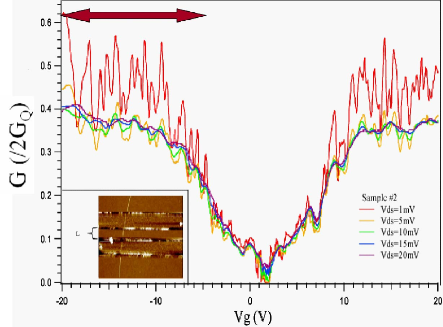
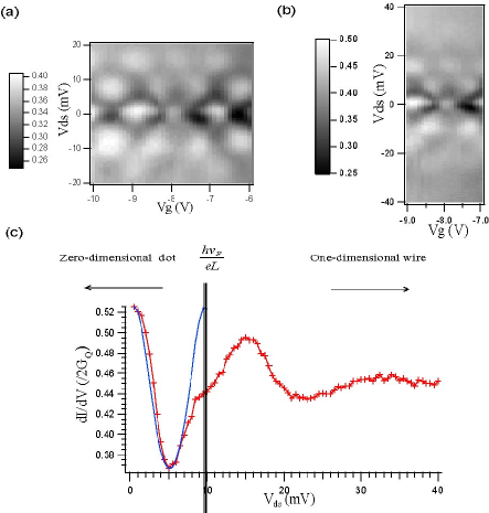
Predictions White98 ; McEuen99 and experiments Bockrath97 ; Liang01 ; Kong01 ; Tans98 have shown that both the elastic and the inelastic mean free path are at least on the order of microns in metallic nanotubes at low temperatures. Electron transport within nm-long SWNTs is believed to be ballistic Liang01 ; Kong01 . We have observed a quantum interference pattern in the differential conductance (where is the drain-source voltage) as a function of and at 4K as shown in Fig. 2(a). The diamond structures are determined by the finite length of the tube between the metal electrodes. The sample is 360 nm-long, and the corresponding energy spacing is roughly 10 meV. The size of the pattern is consistent with the energy spacing. The interference structure continues until approximately mV, above which it fades away (Fig. 2(b)). This interference pattern can be explained by a resonant tunnelling model with quantized energy levels due to finite reflection at the electrode-SWNT interfaces (Fabry-Perot cavity effect) Liang01 .
We consider a simple model to understand the behavior of
. Suppose the interfaces act as potential barriers
with constant transmission probability and . The
energy dependent overall transmission probability is
written for a double-barrier structure as
where is the phase accumulation caused by multiple reflections and a function of and . This simple model fits well the experimental data for a small energy, but deviates significantly as increases (Fig. 2(c)). We can interpret this conductance behavior in terms of the tube length and . The quantum state energy spacing ( ) from the longitudinal confinement is inversely proportional to , , where m/s is the Fermi velocity. When is smaller than , the coherence length of electron wavepackets is longer than L. In this region, the SWNT operates as an isolated zero-dimensional quantum dot between two leads. For , the coherence length of electron wavepackets is shorter than the tube length. In this limit, each wavepacket passes through the one-dimensional conductor, and the oscillating period apparently increases. This phenomenon may indicate the correlated electrons Peca03 .
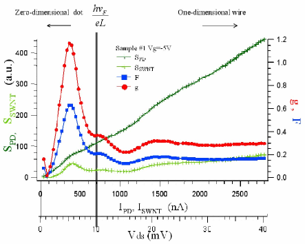
The two-terminal shot noise measurements were implemented by placing two current noise sources in parallel: one is a weakly coupled light emitting diode (LED) and photodetector (PD) pair, and the other is a SWNT. The LED/PD pair, whose coupling efficiency from the LED input current to the PD output current was 0.1 at 4 K, served as the full shot noise source. The high signal-to-noise-ratio was achieved by implementing an AC modulation lock-in technique and a resonant circuit together with a home-built cryogenic low-noise preamplifier Liu98 ; Oliver99 . The input-referred voltage noise was approximately nV at 4 K with a resonance frequency MHz. The signal was fed into a MHz bandpass filter followed by a square-law detector and a lock-in amplifier. The Fano factor was obtained from the ratio of the tube noise () and the full shot noise () at various currents . The current noise generated in the LED/PD pair was measured while the SWNT was voltage-biased at an un-modulated DC current . Figure 3 presents typical data of the measured LED/PD and SWNT shot noise and Fano factor. Two distinct regimes are noticeable depending on the bias voltage . At a low bias voltage ( mV), and oscillates as a function of . For a high bias voltage (mV), and reach saturated values.
The SWNT current fluctuations show many features and can be divided into two distinct regimes according to . A non-interacting electron model predicts that an expected Fano factor is at a net transmission probability . This simple picture, however, does not match the measured over the entire range. In a low , deviates from the non-interacting prediction in a complicated way; the suppressed shot noise around zero becomes enhanced. Enhanced noise would be a consequence of correlated resonant tunnelling Safonov03 . Currents through coherent resonant states may be affected by weak localized states within the system such that additional noise occurs due to interaction. While conductance does not reflect this effect, the shot noise manifests it sensitively.
The SWNT noise in a one-dimensional wire regime is suppressed far below the non-interacting electron prediction. For instance, the tube in Fig. 3 has 14.3k at 40 mV corresponding to and ; however, the observed value at mV is 0.16. Defining this shot noise suppression , the SWNT noise is then written by . The suppression factor (red in Fig. 3.) falls between 0.2 and 0.3 for a large , which matches the theoretical value of the Luttinger parameter in SWNTs Egger97 ; Kane97 .
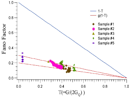
Figure 4 summarizes the Fano factors of five different metallic SWNTs (samples 1-5) as a function of the transmission probability . All values are extracted from the one-dimensional wire regime. For each device, the shot noise measurements were performed by varying . All five tubes manifested both a strong suppression and a consistent value. Surprisingly, even a highly resistive tube also showed a similar suppression (sample 5).
Two different models are considered in an attempt to explain the results. First is the coherent scattering theory (Landauer-B ttiker formalism) Buttiker92 of the non-interacting electrons. in this picture (the blue solid line in Fig. 4) clearly mismatches the experimental result. As the other model, we regard the suppressed shot noise in the context of a Luttinger-liquid model. Although an exact model for the current noise in a non-chiral LL is absent, we phenomenologically combine the partition noise expected from the non-interacting picture with a Luttinger parameter. The Luttinger parameter is predicted to have a value [0.2, 0.3] in carbon nanotubes Egger97 ; Kane97 and, indeed, it was experimentally determined to be from a power-law fit of the conductance in tubes weakly coupled to Fermi reservoirs Bockrath99 . We plotted two linear lines by identification of , i.e. and based on the limiting g values in Fig. 4. Most data points fall between the two lines. In order to test the universality of the additional shot noise reduction factor, the further studies should be needed, for example, the effect of the metal electrode material, the interface between electrodes and tubes and the growth condition of SWNTs.
We would like to point out that of SWNTs increases as decreases in a similar manner to the ballistic conductor except with the additional suppression, which might be related to the electron-electron interactions within the tube. All Fano factors in Fig. 4 were taken at the high . The non-equilibrium noise in an interacting system has not been studied theoretically in this high-energy excitation regime to our best knowledge. A rigorous theoretical work is now in demand to explain the shot noise in individual SWNTs.
We acknowledge Prof. Quate for his encouragement and atomic force microscopes for imaging the SWNT devices and thank the ARO-MURI grant DAAD19-99-1-0215 for support.
References
- (1) C. Dekker, Physics Today 5, 22 (1999).
- (2) M. Bockrath, D. H. Cobden, P. L. McEuen, N. G. Chopra, A. Zettl, A. Thess, and R. E. Smalley, Science 275, 1922 (1997).
- (3) J. Nygard, D.H. Cobden, and P.E. Lindelof, Nature 408 , 342 (2000).
- (4) W. Liang, M. Bockrath, D. Bozovic, J. H. Hafner, M. Tinkham, and H. Park, Nature 411, 665 (2001).
- (5) J. Kong, E. Yenilmez, T. W. Tombler, W. Kim, H. Dai, R. B. Laughlin, L. Liu, C. S. Jayanthi, and S. Y. Wu, Phys. Rev. Lett. 87, 106801 (2001).
- (6) M. Bockrath, D. H. Cobden, J. Lu, A. G. Rinzler, R. E. Smalley, L. Balents, and P. L. McEuen, Nature 397, 598 (1999).
- (7) A. Javey, J. Guo, Q. Wang, M. Lundstrom, and H. Dai, Nature 424, 654 (2003).
- (8) P. G. Collins, M. S. Fuhrer, and A. Zettl, Appl. Phys. Lett. 76, 894 (2000).
- (9) P. -E. Rouche, M. Kociak, S. Gueron, A. Kasumov, B. Reulet, and H. Bouchiart, Euro. Phys. Jour. B 28, 217 (2002).
- (10) M. Büttiker, Phys. Rev. B 46, 12485 (1992).
- (11) R. C. Liu, B. Odom, Y. Yamamoto, and S. Tarucha, Nature 391, 263 (1998).
- (12) W. D. Oliver, J. Kim, R. C. Liu, and Y. Yamamoto, Science 284, 299 (1999).
- (13) X. Maître, W. D. Oliver, and Y. Yamamoto, Physica E 6, 301 (2000).
- (14) G. Burkard, D. Loss, and E.V. Sukhorukov, Phys. Rev. B 61, R16303 (2000).
- (15) P. Samuelsson, E. V. Sukhorukov, and M Büttiker, Phys. Rev. Lett. 91, 157002 (2003).
- (16) R. de Picciotto, M. Reznikov, M. Heiblum, V. Umansky, G. Bunin, and D. Mahalu, Nature 389, 162 (1997).
- (17) E. Comforti, Y. C. Chung, M. Heiblum, V. Umansky, and D. Mahalu, Nature 416, 515 (2002).
- (18) J. Voit, Rep. Prog. Phys. 57, 977 (1994).
- (19) C. Bena, S. Vishveshwara, L. Balents, and M. P. A. Fisher, J. Stat. Phys. 103, 429 (2001).
- (20) B. Trauzettel, R. Egger, and H. Grabert, Phys. Rev. Lett. 88, 116401 (2002).
- (21) K. -V. Pham, F. Piechon, K. -I. Imura, and P. Lederer, xxx.lanl.gov/cond-mat/0207294 (2002).
- (22) H. T. Soh, C. F. Quate, A. F. Morpurgo, C. M. Marcus, J. Kong, and H. Dai, Appl. Phys. Lett. 75, 627 (1999).
- (23) C. T. White, and T. N. Todorov, Nature 393, 240 (1998).
- (24) P. L. McEuen, M. Bockrath, D. H. Cobden, Y. G. Yoon, and S. G. Louie, Phys. Rev. Lett. 83, 5098 (1999).
- (25) S. J. Tans, A. R. M. Verschueren, and C. Dekker, Nature 393, 49 (1998).
- (26) C. S. Peça, L. Balents, and K. J. Wiese, xxx.lanl.gov/cond-mat/0304496 (2003). Rev. B 61, R7869 (2000).
- (27) S. S. Safonov, A. K. Savchenko, D. A. Bagrets, O. N. Jouravlev, Y. V. Nazarov, E. H. Linfield, and D. A. Ritchie, Phys. Rev. Lett. 91, 136801 (2003).
- (28) R. Egger, and A. O. Gogolin, Phys. Rev. Lett. 79, 5082 (1997).
- (29) C. Kane, L. Balents, and M. P. A. Fisher, Phys. Rev. Lett. 79, 5086 (1997).