Modulation of Superconducting Properties by Ferroelectric Polarization in Confined FE-S-FE Films
Abstract
We show that the electric polarization at the interface with ultrathin superconducting (S) films sandwiched between ferroelectric (FE) layers allows achievement of substantially stronger modulation of inner carrier density and superconducting transition temperature as compared to FE-S bilayers typically used in superconducting FETs. We find that not only the larger penetration depths but also the pairing symmetry should be responsible for the fact that the electric field effect in high temperature superconductors is much stronger than in conventional systems. Discussing the advantages of multilayers, we propose a novel design concept for superconducting electric field-effect transistors based on ferroelectric films.
pacs:
74.80.-g,74.80.Dm,77.80.-e,79.60.JvI Introduction
Electric field effect in superconductors continues to attract considerable attention in science and technology ahn . The external field can modulate the charge density and resistance, and control a reversible superconductor-insulator switching behavior which plays a key role in the development of superconducting field-effect transistors (SuFETs) watanabe . Especially in the high-Tc superconducting cuprates, the field effect is expected to be strong, since their low carrier density leads to larger electric field penetration depths nm. Recently, complex ferroelectric oxide materials with high dielectric constant like BaxSr1-xTiO3 (BST) and Pb(ZrxTi1-x)O3 (PZT)ahn2 have been used to achieve substantial carrier modulation and shift of of several K.
Due to the small width of the accumulation layers at the contacts, the effect of the polarization-induced field is most significant in ultrathin superconducting films of a few nanometers thicknessahn ; xi ; ahn2 . With the difficulties related to the fabrication of ultrathin films and interfaces of good quality, theoretical modelling can be an additional effective tool to study these systems. In the bilayer structures, the ferroelectric polarization at the interface attracts or repels the charge carriers in the superconducting film, in close analogy to the effect of doping ahn2 ; watanabe ; logvenov . However, the field effect in FE-S multilayers where the polarization acts on both superconducting surfaces and may strongly modify the internal charge distribution in the entire ultrathin S-film, is a nontrivial and challenging problem. Motivated by recent experimentslogvenov , in this work we show that the use of multilayers can drastically amplify the field effect, hence leading to much stronger increase of the superconducting transition temperature in comparison to S-FE bilayers typically exploited in SuFETs.
II The Model
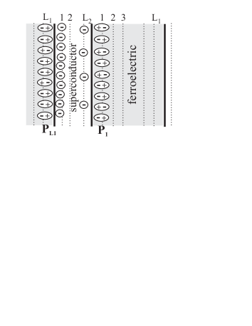
In the approach considered here, we directly describe the internal charge redistribution in a ultrathin S-film caused by the ferroelectric polarization. Assuming the existence of an effectice attractive interaction, we focus on the question of how the superconducting state in the film can be influenced by this polarization. Specifically, we consider a hybrid system composed of periodically alternating FE- and S-layers with the ferroelectric polarization directed perpendicular to the interface, as shown in Fig. 1. The thickness of the FE subsystem is given by the number of monolayers in each ferroelectric layer. In the S-film, denotes the number of
superconducting planes. We propose to describe the structure by the following model:
(i) The two possible orientations of ferroelectric dipoles (shown in
Fig. 1) caused by the ion displacements on each lattice site (unit
cell) of the -th monolayer in the FE-layer can be
described by two values of a pseudospin operator . The
spontaneous polarization below the ferroelectric Curie temperature can
then be modelled by an Ising-type Hamiltonian on the cubic lattice lines :
, where the summation ranges over all nearest
neighboring sites; denotes the internal dipolar interaction potential.
The local polarization is given by the thermal average of and is
assumed to depend only on the monolayer index : .
(ii) In the superconducting film, we consider a
BCS-like pairing in the planes :
| (1) |
The planes are coupled via the interplanar tunneling of the bosonlike pairs,
| (2) |
where the pair operators are
, the
operator creates an electron with spin
and impulse in the -th plane, and
. In
(1), refers to
the electron band energy with lattice constant , and is the chemical
potential. Assuming that some amount of charge
is either
injected into the S-film from the electrodes or already exists due to
chemical doping, we concentrate here on the effect of the carrier
redistribution between the S-planes due to the contact polarization. For -wave pairing,
the superconducting pairing amplitude in each plane
is: , with the
effective pairing potential .
(iii) At the interface we describe the screening of the surface charge due
to the FE-polarization on the surfaces and by the electrons of the S-film.
We consider here only the electrostatic interaction with the electron density
of the boundary S-planes and given by the
electron number operators pavlenko ; pavlenko2 ,
| (3) |
where is the charge-ferroelectric dipole interaction energy. Note that, as the screening length in the cuprate superconductors is about 1 nm, the S-planes close to the boundary S-planes should also be taken into account in (3) in the multilayered cuprates containing more than one CuO2 plane in the unit cellkotegawa with a distance between the planes.
Furthermore, we focus here on the case where the FE-layers are far below the Curie temperature . For this case, we neglect the polarization fluctuations and rewrite the energy in the mean-field approximation, whereas the quasiparticle energies for each given configuration are found by exact numerical diagonalization of the effective S-film energy . The corresponding set of the order parameters and is calculated selfconsistently by minimization of the system free energy. As a result, the proposed procedure describes the inner charge redistribution between the planes of an S-film in effective polarized medium on the boundaries.

The electron-dipole interaction ( and are the electronic and the net FE-unit cell charges) depends on the distance between the nearest FE-monolayers and S-planes. It depends also on the ionic displacement amplitude in the FE-unit cell. For instance, at Å, for a BST-layer with polarization C and Å, we obtain eV, whereas for Å(like in LiNbO3) we get eV. A comparison with the case of a FE-S bilayer is easily provided by fixing the coupling at one of the contacts to zero. In our calculations, we take the pairing potential independent of . Considering the ideal surfaces, we should note that in SuFETs the surface roughness leads to the interface steps with a height unit cell of SrTiO3 as reported in Ref. logvenov, . In the ultrathin S-films, such a step can act as a weak link and strongly affect the in-plane transport wehrli . As long as does not exceed the interplanar distance in the S-film, we can expect our results to not be significantly affected by the rough interfaces, but the problem of transport in this case needs more careful analysis.
III Ferroelectric Polarization
The selfconsistent solutions show stabilization of two different ferroelectric phases (+) and () (discussed in details in Ref. pavlenko, ) with decreasing temperature , depending on the electron concentration and . In phase (+) (Fig. 2), the electric dipoles have the same orientation in each FE-layer (as shown in the inset of Fig. 3(a)), and the substantial deviations of the two possible solutions for () due to the electron screening (3) appear close to the interfaces and decay exponentially beyond the distance of about the ferroelectric correlation lengthpavlenko2 . As seen in Fig. 2, the polarization is also suppressed for smaller FE-layer thickness due to the depolarization field acting on each dipole , however the suppression obtained here is not as crucial as in Ref. ghosez, and we still find a nonzero for a layer with monolayers. To get stronger suppression for a concrete FE-compound, one should consider more realistic long-range dipole-dipole interactions lines as well as strain effects. Nevertheless, we expect our main results related to the superconducting properties robust, since we consider the coupling in the range ( eV for superconducting cuprates) which corresponds to the polarization C obtained in Ref. ghosez, for FE-films of about 10 nm thickness. Also, taking into account the -fluctuations, would suppress the mean-field values of considered in this work as an upper boundary for polarization profiles. With increasing coupling () and for higher electron densities , a transition into the ferroelectric phase () occurs. The fluctuating polarization domainspavlenko appearing in the phase (), are a property of the Ising model in thin films. However, in a specific ferroelectric material these domains could be suppressed due to stronger depolarization fields domains . As the modulation of charge density in this state is much weaker than in phase (+), we focus here only on the polarization in the phase (+) which is of crucial importance for the superconducting properties.
IV Redistribution of Charge in Superconducting Film
In the phase (+), the polarization attracts the charge in the plane () while decreases () as illustrated in Fig. 3(a). At low temperatures, the charge density redistribution due to , can be described by the difference . Consequently, the solution leads to . Moreover, in contrast to the bilayer system, the same direction of in the second FE-layer, say, , repels the charge near the right contact and pushes it towards the accumulation region at the left contact, acting as an additional driving force for the charge supply into the accumulation plane . This results in and which is clearly seen in Fig. 3(a).
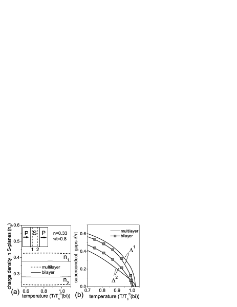
To understand the effect of the inter-planar charge redistribution on the superconducting transition temperature , we consider the case . With the interplanar tunneling , the Hamiltonian (1)-(3) leads to two gap equations in the planes . For -wave symmetry, different local are found:
| (4) |
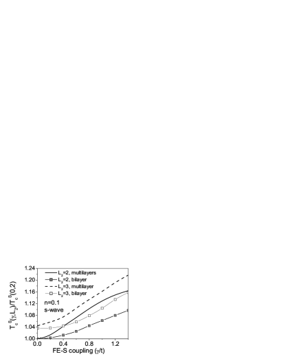
due to the factor caused by the contact polarization. Hence, for low band filling () and for , one finds that and , since the gaps are comparable in energy to . For , this leads to a normal state in the plane , whereas the plane is still superconducting. However, due to the interplanar coupling, even slightly above , the superconducting plane still induces a nonzero for stabilizing the superconductivity in the entire S-film. This effect can be seen in Fig. 3(b) from the numerical solution of the gap equations for . For , both gaps and vanish at a common which is higher than the local calculated for . The enhancement of the pairing on the planes without the pairing interaction solely due to the interplanar coupling is a well known property discussed in the literaturedonovan . In our case, however, the interplanar tunneling plays not only the role of an enhancement factor, but also provides a way for the accumulation of charge and stronger pairing in the accumulation S-plane caused by the polarization. In the multilayers, due to the stronger redistribution of the charge described by , the last property leads to and (Fig. 3(b)). For stronger coupling, the increase of in the multilayer is also substantially stronger than that in the bilayer. The strongest increase of caused by can be achieved for low ; compared to the case (isolated the S-layer), we find a increase of with for , see Fig. 4.
V Inter-planar coupling
To estimate the effect of for , we rewrite the interplanar coupling in (2) in the mean-field approximation and for introduce the order parameters as
| (5) | |||
where the susceptibilities , are the eigenvalues of the mean-field superconducting Hamiltonian, and .
The inter-layer tunneling is introduced in a more generalized form so that the coherent tunneling (2) corresponds to . As the field effect is expected to be stronger in high-Tc superconductors, we consider further the two cases of - and -wave pairing with the ansatz , and in (5). Here for the -wave and for the -wave pairing symmetry. As for we have in the case of isolated S-planes, we assume that the second term in the r.h.s. of the second equation (5) determining is dominant and substitute it into the first equation for . The resulting quadratic equation has the following solution for small :
| (6) |
which corresponds in fact to the upper local transition temperature given in (4) in the limit . However, in contrast to the expressions (4), here due to the inter-planar coupling we note three important features: (i) as analyzed in the literature, the pairing interaction is increased: ; (ii) the factor always leads to an increase of and does not depend on the direction of , demonstrating that the enhancement of is essentially due to the S-planes with the dominant pairing (those with the higher local in (4)); (iii) interestingly, the stronger inter-planar coupling makes the field-effect slightly weaker, since the contribution of in (6) decreases with the increase.

The same effect, i.e. the slightly weaker increase of for larger is also seen in the numerical solution of (5). The most striking fact, however, is that the coupling with the polarization leads to a much stronger increase of in the case of -wave pairing when compared to -wave, shown in Fig. 5. This result suggests that not only the larger screening length, but also the pairing symmetry should be responsible for the much stronger electric field effect in the high-temperature superconductors in comparison with the conventional compounds. Also, the difference between the in the bilayers and sandwiches for the -wave symmetry is much more pronounced which allows us to expect further progress in the field-effect experiments performed with FE-S-FE sandwiches.
VI Scheme of sandwich-based SuFET
Having demonstrated the advantages of sandwiches, we propose a design of a field-effect transistor based on the confined FE-S-FE geometry. The power supply moves the opposite charge to the FE-gate electrodes. The operational principle of such an SuFET consists of two stages: (i) the superconducting state with the enhanced can be reached in the regime where the system has the same direction of in each FE-layer, as illustrated in Fig. 6. Note that for the fixed , the antiparallel polarization in the FE-gates leads to lower charge densities in the accumulation region and consequently to the lower which is discussed in Ref. pavlenko3, . (ii) To switch the SuFET into the insulating state, it is sufficient to destroy the accumulation layer at the first FE-S contact. This can be realized by switching the voltage and tuning the polarization in the FE-layers to zero.
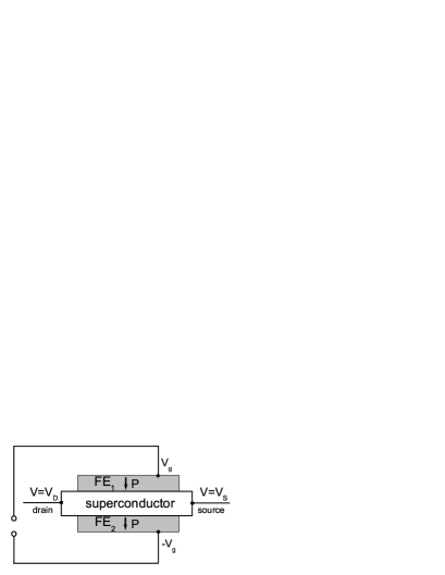
Due to the simple geometry, even at the current stage of fabrication techniques, the proposed SuFETs can be designed and experimentally probed with oxide films as the most promising candidates for high-temperature superconducting electronics. From the above results we expect that in the proposed SuFETs also the effect of charge tunneling between the CuO2-planes could be tested in single- and especially in multilayered cuprates with inhomogeneous carrier distributionkotegawa .
In conclusions, we have shown that the FE-polarization in FE-S multilayers leads to much stronger modulation of inner carrier density and superconducting properties as compared to the bilayers. These advantages of multilayers can be used as the basis of novel design of proposed SUFETs.
Acknowledgements
This work has been supported by the DFG Grants No. SPP-1056 and SFB 484, and by the BMBF Grant No. 13N6918A. The author thanks U. Eckern, J. Mannhart, Yu. Barash, T. Kopp for useful discussions.
References
- (1) C.H. Ahn, J.-M. Triscone, and J. Mannhart, Nature 424, 1015 (2003).
- (2) Y. Watanabe, Appl. Phys. Lett. 66, 1170 (1995).
- (3) C.H. Ahn, S. Gariglio, P. Paruch, T. Tybell, L. Antognazza, J.-M. Triscone, Science 284, 1152 (1999).
- (4) X.X. Xi, C. Doughty, A. Walkenhorst, C. Kwon, Q. Li, and T. Venkatesan, Phys. Rev. Lett. 68, 1240 (1992).
- (5) G.Yu. Logvenov, A. Sawa, C.W. Schneider, and J. Mannhart, Appl. Phys. Lett. 83, 3528 (2003).
- (6) M.E. Lines, A.M. Glass, Principles and Applications of Ferroelectrics and Related Materials (Clarendon Press, Oxford, 1977).
- (7) N. Pavlenko and F. Schwabl, Phys. Rev. B 67, 004313 (2003).
- (8) N. Pavlenko and F. Schwabl, Appl. Phys. A, in press (cond-mat/0309250); N. Pavlenko, Ann. Phys.-Berlin 13, 52 (2004).
- (9) H. Kotegawa, Y. Tokunaga, K. Ishida, G.-q. Zheng, Y. Kitaoka, K. Asayama, H. Kito, Y. Iyo, H. Ihara, K. Tanaka, K. Tokiwa, T. Watanabe, J. Phys. Chem. Solids 62, 171 (2001).
- (10) S. Wehrli and C. Helm, J. Appl. Phys. 95, 5621 (2004).
- (11) J. Junquera and P. Ghosez, Nature 422, 506 (2003).
- (12) The stabilization of the phase () requires equal charge densities on the both boundaries of a FE-layer and thus is expected to be suppressed in the FE-S-FE sandwiches.
- (13) C.O. Donovan and J.P. Carbotte, Phys. Rev. B 55, 1200 (1997); S. Chakravarty et al., Nature 428, 53 (2004).
- (14) N. Pavlenko and F. Schwabl, cond-mat/0407696.