Anomalous temperature-dependent transport in YbNi2B2C
and its correlation to microstructural features
Abstract
We address the nature of the ligandal disorder leading to local redistributions of Kondo temperatures, manifested as annealing-induced changes in the transport behavior of the heavy fermion system YbNi2B2C. The anomalous transport behavior was fully characterized by temperature dependent resistivity measurements in an extended range of K for as-grown and optimally annealed single crystals, and microstructural changes between these two types of samples were investigated by single-crystal x-ray diffraction and transmission electron microscopy. Our results point to lattice dislocations as the most likely candidate to be affecting the surrounding Yb ions, leading to a distribution of Kondo temperatures. This effect combined with the ability to control defect density with annealing offers the possibility of further understanding of the more general problem of the enhanced sensitivity of hybridized Kondo states to disorder, particularly above the coherence temperature.
pacs:
74.70.Dd,75.30.Mb,72.15.QmI Introduction
The transport properties of heavy fermion intermetallic systems often display peculiar behaviorsStewart (1984) whose origin remains as yet unestablished and are subject of current interest. In these systems the effective mass of conduction electrons is enhanced as a result of hybridization between localized electronic orbitals and delocalized conduction bands, and apparently these hybridized states tend to be particularly sensitive to crystalline disorder, manifesting strong sample-to-sample variations in the transport propertiesStewart (1984); Franz et al. (1978) which go beyond trivial differences in residual resistivity.
The quaternary compound YbNi2B2C is a ytterbium-based heavy fermionYatskar et al. (1996); Dhar et al. (1996) with an electronic specific heat coefficient, mJ/mol K2, and a Kondo temperature, K: a temperature scale that is conveniently isolated from other characteristic temperatures such as superconducting or magnetic condensates ( K, if they exist at all), and crystal electric field splitting ( K)Yatskar et al. (1996); Dhar et al. (1996); Grasser et al. (1996); Rams et al. (2000); Boothroyd et al. (2003), and therefore favorable for the study of Kondo physics. Furthermore, an investigation of the effects of annealing on the resistive behavior of boro-carbide single crystalsMiao et al. (2002a) found that YbNi2B2C displayed radical changes in temperature-dependent resistance below room temperature, pointing to the possibility that the transport properties of this compound could be “tuned” to a certain extent by annealing, and thus offer a model system to study the relationship between disorder and hybridized states near the Fermi level.
In a previous reportAvila et al. (2002), we demonstrated a significant variation in the temperature dependent electrical resistivity and thermoelectric power between as-grown crystals and crystals that had undergone annealing at C, whereas the thermodynamic properties (heat capacity and magnetic susceptibility) remained almost unchanged. We interpreted these results in terms of redistributions of local Kondo temperatures associated with ligandal disorder for a small (on the order of 1%) fraction of the Yb sites. This hypothesis left open two obvious questions: (i) What happens to the electrical resistivity for temperatures greater than the maximum possible in this proposed distribution? and (ii) What is the microscopic origin of this distribution of Kondo temperatures?
In the present work, we first extend the temperature range of resistivity measurements both higher (up to 1000 K) and lower (down to 0.4 K), in order to fully characterize the transport behavior of as-grown and optimally annealed crystals and provide further evidence of the proposed model. We then present x-ray single-crystal refinements and transmission electron microscopy experiments, which provide new information on the types of disorder that may be causing the anomalous Kondo temperatures in the surrounding Yb sites.
II Experimental Details
Single crystals of YbNi2B2C were grown from Ni2B flux at high temperatures as described elsewhereCanfield et al. (1998); Yatskar et al. (1996). For the resistivity measurements, a particularly clean and well-formed single crystal plate measuring approximately mm3 was selected, polished on both surfaces to remove most of the attached flux, and cut using a wire saw into flat bars of typical dimensions mm3 with the length along the [100] direction. Electrical contacts were placed on three unannealed samples in standard 4-probe linear geometry, using Pt wires attached to a sample surface with Ablebond 88-1 silver epoxy. For each slab, the sample weight and dimensions were carefully measured and an evaluation of the sample densities ( g/cm3) was used to estimate an upper limit of for the overall geometry-related uncertainty in calculating resistivity , where is the cross-sectional area and is the distance between voltage leads.
Two measured samples were then selected to undergo annealing for comparison. The Pt wires were removed and the silver epoxy was polished off, leading to a small () decrease in the sample’s original weight due to an intentional, slight overpolishing. Since the polishing occurred on a single flat surface parallel to the current direction, the reduction in the sample cross-section was assumed to be the same as the one in mass. The samples were then annealed in vacuum for 150 hours at C (details of the annealing procedure are described in ref. Avila et al., 2002).
Electrical resistance measurements below room temperature were performed on commercial Quantum Design PPMS systems, allowing measurements down to 1.8 K, or down to 0.4 K if the 3He option is installed. Above room temperature, measurements were performed on a custom-built high temperature resistivity system (HTRS) which can be mounted on the same system used for sample annealing under vacuum ( Torr). A quartz probe is inserted in the system with four leads where the other end of the sample contacts are attached using silver epoxy. Temperature is measured with two independent thermometers: Pt resistance temperature detector (RTD) and type-R thermocouple. A 1 mA current is applied on the sample by a Keithley 220 current source and the voltage is read on a HP 34420A nanovoltmeter. The RTD current is applied by a LakeShore 120 current source and the voltage is read on a HP 34401A multimeter. The thermocouple voltage is read by another HP 34420A nanovoltmeter. All these instruments are GPIB interfaced with a computer running a custom-made software for data acquisition. To reduce noise and avoid diode or thermoelectric effects, five readings are taken with the current in each direction, and the ten absolute voltage values are averaged.
A typical HTRS experiment proceeds as follows. 1) The system is heated to 450 K for about an hour in air to cure the contacts, then cooled back to room temperature. 2) The vacuum system is turned on and allowed to achieve a dynamic vacuum of Torr or better. 3) The furnace temperature is ramped at 2 K/min or slower up to about 600 K and back to room temperature, while the software acquires data points every 2 min. This first ramp is used to allow further stabilization of the contacts which often undergo small changes when heated, marked by irreproducible shifts in the resistance behavior. 4) The definitive dataset is acquired by ramping at 2 K/min or slower up to about 1000 K and back to room temperature, while the software acquires data points every 2 min. For the same reason of contact stability and in order to obtain a good match between the curves from both measurement systems, the low temperature measurements in the PPMS were performed only after the high temperature ones, and for each sample the data presented in figures 1 and 2 is the cool down from 1000 K to 300 K in the HTRS, followed by the cool down from 300 K to 1.8 K or 0.4 K in the PPMS. A certain level of mismatch still remains at room temperature, both for the absolute value of the measured resistance and for its slope, but these differences are considered small enough to be neglected in the comparative analysis we present in this work.
For the crystallographic studies, room temperature X-ray diffraction (XRD) data of as-grown and annealed YbNi2B2C single crystals were collected using a Bruker APEX diffractometer with Mo radiation ( Å) and a detector-to-crystal distance of 5.08 cm. Data were collected for the full sphere and were harvested by collecting three sets of frames with 0.3∘ scans in for an exposure time of 10 seconds per frame. The range of extended from 3.0∘ to 56.0∘. Data were corrected for Lorentz and polarization effects; absorption corrections were based on fitting a function to the empirical transmission surface as sampled by multiple equivalent reflections. Unit cell parameters were indexed by peaks obtained from 90 frames of reciprocal space images and then refined using all observed diffraction peaks after data integration. Together with systematic absences, the space group (N. 139) was selected for subsequent structural analysis. The structure solution was obtained by direct methods and refined by full-matrix least-squares refinement of using the SHELXTL 6.10 packageSheldrick (2000).
For the transmission electron microscopy (TEM) evaluations, the as-grown and annealed single crystals of YbNi2B2C were characterized using a Philips CM30 transmission electron microscope operating at 300 keV. The single crystals were placed in a mortar with denatured ethyl alcohol and ground to a fine powder. A pipette was used to place a small drop of the suspension onto a holey carbon grid. The suspension was air-dried before insertion into the microscope. The crystalline structure of fragments which were electron transparent was evaluated using selected area electron diffraction pattern (SADP). The defect density was measured on select areas of the bright-field images where the thickness was relatively uniform.
III Resistivity Measurements
The main motivation for extending the resistivity measurements to high temperatures was based on the assumption that, if the excess scattering seen at room temperature and below in unannealed samples arises from the contribution of Yb sites with Kondo temperatures extending up through room temperature, there should be a temperature above which the samples no longer display anomalous scattering, and the difference between the resistivity of unannealed sample and the annealed sample becomes a “simple” Matthiessen impurity term.
The temperature dependence of the electrical resistivity for three unannealed pieces of YbNi2B2C cut from the same crystal is shown in Fig. 1. The general behavior below room temperature is the same as has been previously reported for as-grown samples of this compound,Miao et al. (2002a); Avila et al. (2002); Bud’ko et al. (1997); Hossain et al. (1997); Yatskar et al. (1999); Rathnayaka et al. (1997) i.e., a high-scattering metallic behavior down to about 30 K, below which the resistivity decreases rapidly. If normalized to their respective resistance values at any given temperature, these three curves essentially collapse into a single one in the entire measured temperature interval, meaning that the selected crystal was quite homogeneous and the differences seen in the three measurements result from the overall % uncertainty in estimating the geometrical factor for each piece. The residual resistivity ratio (defined as ) is for all three samples, somewhat higher than found for several other unannealed crystals grown similarly Miao et al. (2002a); Avila et al. (2002), indicating that by measuring the high temperature region first we are already annealing out a small portion of the disorder, but still maintaining most of the characteristic unannealed sample behavior.
A crystal of LuNi2B2C was also measured to provide a reference for the non-magnetic (e.g. standard electron-phonon) contribution to scattering down to 16 K, below which it becomes superconducting. The high temperature region is somewhat noisier for this sample because its cross-section is about 3 larger than the others and therefore the actual measured resistance is proportionally smaller. On the other hand, the uncertainty in this sample’s geometrical factor is equally smaller, so its slope becomes a good reference. It is interesting to note that, assuming cm Å for LuNi2B2C,Cheon et al. (1998) near 1000 K the measured resistivity of order cm implies a mean free path Å, already comparable to the unit cell lattice parameter (the Ioffe-Regel criterion), however the resistivity behavior is still quite linear with a slope cm/K between 600 K and 900 K. Above 600 K, all three YbNi2B2C samples change slope and roughly follow that of the LuNi2B2C sample (except for the nearly constant extra magnetic contribution).

Samples 1 and 3 were then annealed for 150 hours at 950∘C and remeasured. Figures 2a and 2b present the comparison between unannealed and annealed resistivity for each sample. Let us go through the comparison in detail for sample 1. At high temperatures (above about 600 K), the curves for the unannealed and annealed conditions of the sample run essentially parallel to each other (and roughly parallel to LuNi2B2C), meaning that in this region there is simply a temperature-independent resistivity factor , in accordance with Matthiessen’s rule. As we cool below 600 K the unannealed curve maintains a more slowly decreasing resistivity (or, conversely, a increased level of scattering), when compared to the other two which continue to run parallel down to about 200 K. Around this temperature the annealed YbNi2B2C curve presents a broad shoulder, most likely related to the thermal depopulation of the CEF multiplet with K, and therefore approaches the LuNi2B2C curve. Between 50 K and 10 K the resistivity of the annealed sample resembles a Kondo-minimum type behavior, and below 10 K its resistivity once again drops rapidly due to the onset of coherent scattering of the Yb ions, making its final approach towards the conventional scattering level of the normal-state, non-magnetic LuNi2B2C. Qualitatively similar results are found for sample 3. For both YbNi2B2C samples increased to 17 with annealing, consistent with the previous results from annealed crystalsAvila et al. (2002).

Following the encouraging results above, we remeasured these samples in the PPMS with the 3He option in order to extend the resistivity curves down to our lowest measurable temperatures, so as to check how annealing affects the behavior in this regime and verify whether or not they follow the theoretical predictions for a Fermi-liquid.
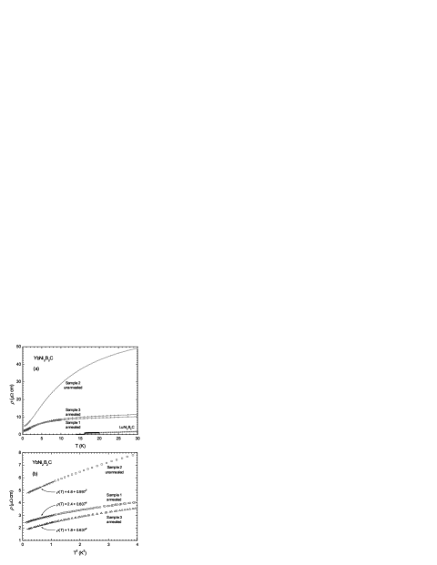
In figure 3a we show the temperature dependence of resistivity below 30 K of sample 2 which was left unannealed, and samples 1 and 3 (annealed). The decrease in resistivity below 10 K is quite evident in the annealed samples, whereas the resistivity of the unannealed one is already decreasing rapidly below 30 K. In figure 3b we plot the same data in the region below 2 K as a function of , and all three curves are slightly sub-linear in this plot, indicating that they cannot be completely described by a Fermi-liquid type relation in this temperature range. In the graph we have included a fit of this expression to the three datasets below 1 K. It seems that with the decrease in disorder there is a decrease in both and . The only other investigations of this type previously reported on an unannealed crystalYatskar et al. (1997, 1999) resulted in cm, and are consistent with this trend. Such a large reduction in is not expected within the framework of the Fermi-liquid models, since our previous studyAvila et al. (2002) found that the electronic specific heat coefficient changes very little with annealing (no more than 10% for the lowest measured temperatures). Even taking into account this small change in , the ratio still decreases from to cm (mol K/mJ)2 with annealing. These values are smaller than the Kadowaki-Woods ratioKadowaki and Woods (1986) of cm (mol K/mJ)2 found empirically for many Fermi-liquid systems.
The difference of 2-3 cm in between our annealed and unannealed YbNi2B2C samples is similar to the results obtained by annealing studies on non-hybridizing TmNi2B2CMiao et al. (2002b) and also comparable to the results of Lu(Ni1-xCox)2B2C substitution studiesCheon et al. (1998) when . These similarities suggest that the optimal annealing of single crystals grown by the Ni2B flux growth method is essentially removing lattice imperfections on the order of 1%, and in the coherent scattering regime YbNi2B2C behaves like all other members of the family. Furthermore, the difference in resistivity between annealed and unannealed samples above 600 K (Fig. 2) was found to be 3-6 cm, which is remarkably similar as well (considering that the separations between the resistivity curves are strongly affected by geometrical uncertainties at these high temperatures) and therefore once again points to the return of a more conventional scattering regime at very high temperatures.
Given the consistency of the extended transport measurements with the hypothesis that ligandal disorder in the as-grown samples is leading to redistributions of Kondo temperatures for a small fraction of the Yb sites, the question that arises naturally is: what are the types of disorder contributing to this behavior? To address this question, we now present a series of structural and microscopic experiments conducted on as-grown and annealed single crystals.
IV Single Crystal X-Ray Refinements
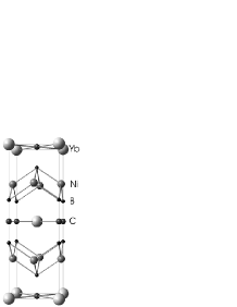
The single-crystal XRD technique is useful to check for vacancies, substitutions, superstructures, and other perturbations of periodic atomic sites in the crystal. The structure refinement for the as-grown and annealed YbNi2B2C was carried out under the assumption that no structural disorder was present. By this assumption all systematic absences pointed to the expectedSiegrist et al. (1994a) crystal system (Tetragonal) and space group () represented in figure 4. Atomic positions were assigned based on site symmetry and bond length and agree with previously published single crystal data for other Ni2B2C series membersSiegrist et al. (1994b). However, subtle problems with the initial structure refinement of the as-grown samples implied that the solution was not complete.
For most crystal structure refinements a parameter is added to account for the accordance of extinction. In the SHELXTL software the extinction parameter accounts for both primary and secondary extinctionSheldrick (2000). Before the extinction parameter was added to the refinement of the as-grown YbNi2B2C the R-index was 0.1224 and the thermal parameters for Yb and B were not convergent (table 1). After the extinction parameter was added the refinement appeared to be stable with the exception of the C thermal parameter (this is typical for light elements in the presence of heavy elements). However, the extinction parameter itself (0.24(2)) is larger than what is normally expected (table 2). In solid state structures a large extinction parameter usually indicates the existence of a super-cell structure. Because super-cell structural solutions were not found in this case, as indicated by the absence of additional reflections, the large extinction parameter is most likely due to the presence of dislocations. Refinement of the annealed YbNi2B2C structure presented no problems (extinction parameter 0.065(8)), suggesting that much of the disorder present in the sample before the annealing process has been removed. There is no evidence of vacancies or substitutions within the resolution limit of this technique.
| Yb | 0 | 0 | 0 | 0.00001 |
|---|---|---|---|---|
| Ni | 0 | 0.5 | 0.25 | 0.00258(1) |
| B | 0 | 0.5 | 0.360(7) | 0.00001 |
| C | 0.5 | 0.5 | 0 | 0.00917(1) |
| Yb | 0 | 0 | 0 | 0.0076(7) |
|---|---|---|---|---|
| Ni | 0 | 0.5 | 0.25 | 0.0066(6) |
| B | 0 | 0.5 | 0.360(7) | 0.0061(3) |
| C | 0.5 | 0.5 | 0 | 0.00001 |
| Yb | 0 | 0 | 0 | 0.0052(6) |
|---|---|---|---|---|
| Ni | 0 | 0.5 | 0.25 | 0.0042(6) |
| B | 0 | 0.5 | 0.361(2) | 0.0044(4) |
| C | 0.5 | 0.5 | 0 | 0.0065(4) |
V Transmission Electron Microscopy

In order to obtain a more detailed and quantitative estimate of these dislocations we studied the TEM patterns of crushed crystals. Figure 5(a) and (b) show two representative bright field TEM images and the corresponding SADPs (insets) of the crushed as-grown and annealed YbNi2B2C single grains, respectively. Both SADPs are fully consistent with the known space group ( (139)) for this compound, and they do have a common reciprocal lattice vector, (110), which is approximately equal for these two samples. There are no obvious second phases and the diffraction spots are sharp, indicating well crystallized samples. However, the as-grown crystallites show a surprisingly large number of dislocations (Fig. 5a). In contrast, the annealed samples while exhibiting some regions of moderate defect density, the defect density is qualitatively lower than the as-grown sample. Using an estimated thickness of 800 and 500 nm for the as-grown and annealed samples, we estimate a defect density of and cm-2 for the as-grown and annealed samples, respectively.
Although it is not expected that room temperature crushing of a nominally brittle intermetallic would result in extensive dislocation formation, it is not without precedenceBeraha et al. (1997). The difference in the dislocation density between the as-grown and annealed samples may be due to the presence of Frank-Read sources, small defects which when subjected to high shear stresses are capable of overcoming the Peierls forces resisting dislocation mobility. This would imply that the as-grown crystals may have many small, and hard to detect defects which are eliminated by annealing.
VI Discussion
In our previous studyAvila et al. (2002) we made a semi-quantitative evaluation of the fraction of Yb sites that would need to be perturbed in order to account for the excess resistivity seen at room temperature and below in the unannealed samples. Using the expression for the increase in resistivity caused by a Kondo impurity for temperatures below the Kondo temperature associated with the impurityAvila et al. (2002); Thompson and Fisk (1985):
where is the concentration of Yb “impurities”, is the Fermi momentum, is the number of electrons per atom, and is the ytterbium angular momentum, we estimated an increase in the room temperature resistivity of about for every 1% concentration of affected Yb sites with greater than 300 K. The extended resistivity measurements and analysis performed in the present work have confirmed and reinforced that initially proposed semi-quantitative model. We have observed that when the sample is well into the coherent scattering regime ( K) or well above the maximum perturbed Kondo temperature ( K) the Yb ions behave like the more conventional, non-hybridizing rare-earth members in the Ni2B2C series and the overall resistivity decrease with annealing is of only 2-3 , once again consistent with a density of order 1% of conventional scattering sites.
The TEM experiments clearly showed the presence of defects in both unannealed and annealed samples most likely associated with lattice dislocations, and the defect density was estimated to be at least 2.5 times larger in the unannealed samples. Similar qualitative changes were seen in the XRD data. With these results we can propose a scenario where the dislocation sites act as a source of strain fields which disturb nearby Yb sites with intensity inversely proportional to their distance to the defect origin, which would then lead to the appearance of a distribution of local Kondo temperatures along the strain field decay. Estimating the extension of a strain field around a dislocation core is complicated, and will vary according to the nature of the dislocation, the modulii of the material and the length of the Burger’s vector. However, we can once again attempt a semi-quantitative analysis. Using the defect density of cm-2 for the unannealed sample and assuming that 1% of the Yb sites are subject to a strain field, we can estimate that all Yb sites within a radius of Å of each dislocation core would be feeling the effect of the strain field. This value corresponds to about 130 unit cells along the plane and 40 unit cells along the -axis, and seems rather large given that, according to Eshelby and othersHirsch (1975), the region of elastic limit should be on the order of 5 times the Burger’s vector. For our samples the dislocations appear to be of the type with corresponding Burger’s vector Å. We can still argue an enhanced sensitivity of the hybridized Yb ions to the strain, but even so it is likely that the extension of the strain field (or the fraction of affected Yb sites) is being overestimated.
Whereas there are very clear changes in the microstructural data (TEM and single-crystal XRD) with annealing, the link between these changes and the changes in the transport measurements remains only semi-quantitative.
VII Conclusion
In this work we have fully characterized the resistivity behavior of annealed and unannealed YbNi2B2C single crystals in the range of K. Whereas the variability of resistivity behavior for compounds with hybridizing moments has been long suspected, our studies on YbNi2B2C finally allow a clear and controlled demonstration of this effect. We were also able to use single crystal XRD and TEM data to gain confidence in the claim that the changes are indeed intrinsic to the compound which is clearly single phase in both annealed and as-grown conditions. For this particular material and growth process, lattice dislocations seem to be the dominant defect type found in as-grown crystals, and is most likely being responsible for environment changes in the nearby Yb3+ ions which lead to deviations of local Kondo temperatures from their intrinsic value of K. As a consequence, it is important to realize that any attempt at detailed analysis of transport properties such as those found for YbNi2B2C (and these are not uncommon) are highly suspect, and any comparison of experiments with theoretical models must either take into account the sensitivity of the hybridizing moments on the modelling side or guarantee a nearly defect-free sample, a highly non-trivial experimental requirement.
Acknowledgements.
We are thankful to F. Borsa for urging us to measure the high-temperature of YbNi2B2C, to J. Schmalian for stimulating discussions, to I. R. Fisher and T. Wiener for the development of the high-temperature resistivity system, and to Y. Mozharivskyj for assistance with the x-ray refinements. Ames Laboratory is operated for the US Department of Energy by Iowa State University under Contract No. W-7405-Eng-82. This work was supported by the Director for Energy Research, Office of Basic Energy Sciences.References
- Stewart (1984) G. R. Stewart, Rev. Mod. Phys. 56, 755 (1984).
- Franz et al. (1978) W. Franz, A. Griessel, F. Steglich, and D. Wohlleben, Z. Phys. B 31, 7 (1978).
- Yatskar et al. (1996) A. Yatskar, N. K. Budraa, W. P. Beyermann, P. C. Canfield, and S. L. Bud’ko, Phys. Rev. B 54, R3772 (1996).
- Dhar et al. (1996) S. K. Dhar, R. Nagarajan, Z. Hossain, E. Tominez, C. Godart, L. C. Gupta, and R. Vijayaraghavan, Solid State Commun. 98, 985 (1996).
- Grasser et al. (1996) U. Grasser, P. Allenspach, F. Fauth, W. Henggeler, J. Mesot, A. Furrer, S. Rosenkranz, P. Vorderwisch, and M. Buchgeister, Z. Phys. B 101, 345 (1996).
- Rams et al. (2000) M. Rams, K. Krolas, P. Bonville, J. A. Hodges, Z. Hossain, R. Nagarajan, S. K. Dhar, L. C. Gupta, E. Alleno, and C. Godart, J. Magn. Magn. Mater. 219, 15 (2000).
- Boothroyd et al. (2003) A. T. Boothroyd, J. P. Barratt, P. Bonville, P. C. Canfield, A. Murani, A. R. Wildes, and R. I. Bewley, Phys. Rev. B 67, 104407 (2003).
- Miao et al. (2002a) X. Y. Miao, S. L. Bud’ko, and P. C. Canfield, J. Alloys Compnds. 338, 13 (2002a).
- Avila et al. (2002) M. A. Avila, S. L. Bud’ko, and P. C. Canfield, Phys. Rev. B 66, 132504 (2002).
- Canfield et al. (1998) P. C. Canfield, P. L. Gammel, and D. J. Bishop, Physics Today 51, 40 (1998).
- Sheldrick (2000) G. M. Sheldrick, SHELXTL, version 6.10 (Bruker AXS Inc., Madison, WI, 2000).
- Bud’ko et al. (1997) S. L. Bud’ko, P. C. Canfield, A. Yatskar, and W. P. Beyermann, Physica B 230-232, 859 (1997).
- Hossain et al. (1997) Z. Hossain, R. Nagarajan, S. M. Pattalwar, S. K. Dhar, L. C. Gupta, and C. Godart, Physica B 230-232, 865 (1997).
- Yatskar et al. (1999) A. Yatskar, C. H. Mielke, P. C. Canfield, A. H. Lacerda, and W. P. Beyermann, Phys. Rev. B 60, 8012 (1999).
- Rathnayaka et al. (1997) K. D. D. Rathnayaka, D. G. Naugle, S. Lim, M. C. de Andrade, R. P. Dickey, A. Amann, M. B. Maple, S. L. Bud’ko, P. C. Canfield, and W. P. Beyermann, Int. J. Mod. Phys. 13, 3725 (1997).
- Cheon et al. (1998) K. O. Cheon, I. R. Fisher, V. G. Kogan, P. C. Canfield, P. Miranovic, and P. L. Gammel, Phys. Rev. B 58, 6463 (1998).
- Yatskar et al. (1997) A. Yatskar, S. L. Bud’ko, P. C. Canfield, W. P. Beyermann, G. M. Schmiedeshoff, M. S. Torikachvili, C. H. Mielke, and A. Lacerda, Physica B 230-232, 876 (1997).
- Kadowaki and Woods (1986) K. Kadowaki and S. B. Woods, Solid State Commun. 58, 507 (1986).
- Miao et al. (2002b) X. Y. Miao, S. L. Bud’ko, and P. C. Canfield, unpublished results related to ref. Miao et al., 2002a (2002b).
- Siegrist et al. (1994a) T. Siegrist, H. W. Zandbergen, R. J. Cava, J. J. Krajewski, and W. F. Peck, Nature (London) 367, 146 (1994a).
- Siegrist et al. (1994b) T. Siegrist, R. J. Cava, J. J. Krajewski, and W. F. Peck, J. Alloys Compnds. 216, 135 (1994b).
- Beraha et al. (1997) L. Beraha, M. Duneau, H. Klein, and M. Audier, Phil. Mag. A 76, 587 (1997).
- Thompson and Fisk (1985) J. D. Thompson and Z. Fisk, Phys. Rev. B 31, 389 (1985).
- Hirsch (1975) P. B. Hirsch, The Physics of Metals (Cambridge University Press, 1975), vol. 2 Defects, p. 302.