Thermoelectric properties of junctions between metal and models of strongly correlated semiconductors
Abstract
We study the thermopower of a junction between a metal and a strongly correlated semiconductor. Both in the electronic ferroelectric regime and in the Kondo insulator regime the thermoelectric figures of merit, , of these junctions are compared with that of the ordinary semiconductor. By inserting at the interface one or two monolayers of atoms different from the bulk, with a suitable choice of rare-earth elements very high values of can be reached at low temperatures. The potential of the junction as a thermoelectric device is discussed.
pacs:
72.10.Fk, 73.40.Cg, 73.40.Ns, 73.50.LwI Introduction
New thermoelectric coolers and power generators are under massive investigation.physicstoday These devices are in general even more reliable than commercial heat-exchange refrigerators but their efficiency, in the best cases, is much lower. The quality of the material need in a thermoelectric device is defined by the dimensionless figure of merit , where is the absolute temperature, and is expressed in Eq. (1) in terms of transport coefficients. Currently, the highest value of , which is 1 at room temperature, is found in Bi-Te alloys.superrama New devices would be competitive with traditional refrigerators if were about 3 4: the major lack of high- materials is at temperatures below 300 K.
In this paperus we propose a junction of metal and strongly correlated semiconductor as the basis for a possible efficient low-temperature thermoelectric device. This system embodies previous intuitions that were recognized fruitfulsales ; procnat ; optimumgap ; mao ; 2d ; 2d2 ; 2d3 ; mahan2d ; nahum ; edwards ; thermionic ; moyzhes ; min in different materials/devices such as rare-earth compounds, superlattices, and metal/superconductor junctions. We now outline these concepts and briefly review the related literature.
From the definition
| (1) |
where is the absolute thermopower (Seebeck coefficient), the electrical conductivity, and and the electronic and lattice part, respectively, of the thermal conductivity, it follows that an ideal thermoelectric material should have high thermopower, high electrical conductivity, and low thermal conductivity. Semiconductors seemed to have the optimum collection of these properties, in contrast with metals, which have high but low , and insulators, which have high but low . However, in the last thirty years no substantial enhancement of beyond 1 was obtained.
A breakthrough came with the synthesis of new materials such as filled skutterudites, which have nearly bound rare-earth atoms, closed in an atomic cage, whose “rattling” under thermal excitation scatters phonons, then dramatically reducing .sales More generally, heavy atoms in compounds help with lowering . Mahan and Sofoprocnat also showed that the best bulk band structure for high is one with a sharp singularity in the density of states very close to the Fermi energy. These results provide the first idea in the search for the best thermoelectric, namely to look at rare-earth compounds as major candidates. In fact, mixed valence metallic compounds (e.g. CePd3, YbAl3) show high values of , but at the present time no useful value of has been reported.rareearth
The second idea is that the best thermoelectric must have an energy gap. Because in ordinary semiconductors the optimum band gap is predicted to be about 10 ( being the Boltzmann constant),optimumgap one is led to consider small-gap semiconductors for low-temperature applications. If the chemical composition of semiconductors includes transition metals or rare earths, conduction and valence bands are frequently strongly renormalized by correlation effects, forming a temperature-dependent gap (see Fig. 2): this is the case for mixed-valent semiconductors, usually cubic, whose relevant electronic properties may be modeled by a -flat band and a broad conduction band, with two electrons per unit cell.kondo This class of materials consists of two subclasses: The first is the Kondo insulator, characterized by very strong Coulomb interaction between electrons on the same rare-earth site, usually described by the slave boson solution of the Anderson lattice hamiltonian.slaveboson ; quasiferro Mao and Bedell predicted a high value of for bulk Kondo insulators (the lower the dimension, the higher the value):mao however, some experimental reports seem to exclude this possibility.physicstoday ; kondom ; kondom2 The second, called the electronic ferroelectric (FE),ferro consists of semiconductors with high dielectric constants, such as SmB6 and Sm2Se3, and it is modeled by the self-consistent mean-field (MF) solution of the Falicov-Kimball Hamiltonian.Falicov The ground state of the insulating phase is found to be a coherent condensate of -electron/-hole pairs, giving a net built-in macroscopic polarization which breaks the crystal inversion symmetry and makes the material ferroelectric.ferro
Another useful observation is that is reasoned to increase in quantum-well superlattices, due to the modification of the density of states.2d ; 2d2 ; 2d3 Moreover, superlattices with large thermal impedance mismatch between layers seem very efficient at reducing because interfaces scatter phonons very effectively.mahan2d However, if the transport is parallel to the layers, the parasitic of the bigger gap materialphonom1 ; phonom2 or the tunnelling between conduction layersphonom2 can drastically decrease . Besides, if intra-layer transport is diffusive and described by bulk parameters, for the whole superlattice cannot be higher than the maximum value for the single constituents.toobig
In addition to the above literature, this work was stimulated by some recent advances in thermoelectric applications of junctions. Nahum and coworkersnahum built an electronic microrefrigerator based on a metal-insulator-superconductor (NIS) junction. Subsequent experimentalpekola and theoretical workedwards ; averin ; hirsch confirmed this new idea. Edwards and coworkersedwards showed that tunneling through structures with sharp energy features in the density of states, like quantum dots and NIS junctions, can be used for cryogenic cooling. It seems then a natural extension to us to study the junction between a metal and a strongly correlated semiconductor.
There were recent proposals for devices such as semiconductor/metal superlattices with transport perpendicular to interfaces. Mahan and Woodsthermionic suggested a multilayer geometry with the thickness of the metallic layer smaller than the electronic mean free path and the semiconductor acting as a potential barrier (thermionic refrigeration). Independently, Moyzhes and Nemchinskymoyzhes proposed a similar configuration with the metallic layer thickness comparable with the energy relaxation length. We cite also Min and Rowe’s ideamin of using Fermi-gas / liquid interfaces. While the analysis of electronic transport of Ref. thermionic, and moyzhes, is not applicable to our study, because of the sharp energy profile of the transmission coefficient across the junction which we examine, and of the nature of the correlated semiconductor ground state, this experimental geometry, with the strongly correlated semiconductor replacing the barrier layer, could be implemented, as we suggest at the end of Sec. IV.3.
In sum, we build on two key ideas from the above literature for increasing . One is to utilize the sharp energy features in the density of states of bulk materials as in strongly correlated semiconductors. The other is to exploit the good thermoelectric characteristics of a junction. In this paper, we combine these ideas in exploring the thermopower behavior of a junction between a metal and different classes of semiconductors. We describe the gapped material on one side of the junction as the solution of the Falicov-Kimball HamiltonianFalicov in different regimes. In particular, we consider the case of: (i) Electronic Ferroelectric (FE), where, because of the Coulomb interaction between -holes and -electrons, the MF insulating ground state is a condensate of excitons;ferro (ii) Narrow Band semiconductor (NB), characterized by the - band hybridization: it would be a Kondo insulator had we take into account the - electron repulsion; (iii) Broad band semiconductor (SC), for comparison. In these three cases, we solve the electronic motion across the junction by means of a two-band model analogous to the Bogoliubov-de Gennes equationsDegennes in a finite-difference form. In addition to the clean interface, we consider an “impurity” overlayer made either of rare-earth atoms, with relevant atomic orbitals of -type, or of atoms with -type orbitals, like transition metals. In the latter case, electrons can hop from these “-impurity” sites to adjacent neighbor atoms, while in the former -impurity case hopping is assumed negligible. This scenario is motivated by recent advances in atomic layer fabrication. We compute for the interface via a linear response. We find that can be greatly enhanced by the presence of a suitable -impurity layer at the interface. In particular, for a fixed working temperature of the junction, an optimum energy of the -impurity level exists which maximizes , especially at low temperatures. In these regimes, bulk thermal conductivity would be dominated by phonons which would reduce . However, one can fabricate the junction with two materials with large thermal impedance mismatch, so that phonon scatterings at the interface decrease the thermal conductivity. Thus, phonon conductivity would not diminish the high found. To this aim we propose an experimental setup, namely perpendicular transport in metal/FE superlattice.
The structure of the paper is as follows: in Section II we describe the model Hamiltonian, in Sec. III.1 we solve the electronic motion across the junction, and in Sec. III.2 we compute transport coefficients and . In Sec. IV we present and discuss our results, for the clean interface (IV.1), and for the - (IV.2) and - (IV.3) impurity layer. Also we briefly discuss some structural relaxation effects of the interface (sec. IV.4). Our conclusions are in Sec. V.
II The model
We introduce the one-dimensional spinless Hamiltonian to model the motion across the junction along the direction perpendicular to the interface between a metal and different types of semiconductor. is given by the sum of three terms:
| (2) |
is a tight-binding Hamiltonian describing the metal on the left side of the junction:
| (3) |
Here destroys an electron of charge at the lattice site with energy and position , is the lattice constant, is the hopping parameter for nearest-neighbor sites, and is the electrostatic potential across the junction by applying an external bias. In our model, is constant in the two bulk regions with a discontinuous step at the interface, although the actual profile should be determined self-consistently together with the electronic density.
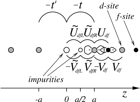
The third term in Eq. (2) is the Falicov-Kimball HamiltonianFalicov referring to the insulator on the right side of the interface. In addition to the Coulomb interaction between the -electrons at sites and the -electrons localized on atoms at , we add a hybridization term ( is the modulus of the hybridization integral) between and orbitals. Because the crystal has inversion symmetry, this term has to be odd, namely the hybridization term between sites at and and that between sites at and have opposit sign (see Fig. 1):
| (4) |
| (5) | |||||
| (6) | |||||
where is the hopping coefficient, and and are the - and -site energies, respectively.
The second term in Eq. (2) is the Hamiltonian at the interface, which describes the overlayer made of -sites at and -sites at :
| (7) | |||||
Here we have included the possibility of “impurity” atoms at the interface, namely one with average energy at position and another one with energy at position . Since the impurity atoms have orbitals differing from those in the bulk, the associated and parameters generally change. We denote them by , , , and , referring to the couples of sites and , respectively (Fig. 1).
We give the MF solution of the Hamiltonian of Eq. (2), by means of an approach (see Sec. III.1) analogous to the Bogoliubov-de Gennes methodDegennes (BdG). In contrast to the electron-electron pairing in the Bardeen-Cooper-Schrieffer (BCS) MF theory of superconductivity, the pairing here occurs between -electrons and -holes. To proceed, we assume that
| (8) |
| (9) |
| (10) |
| (11) |
| (12) |
| (13) |
Here is the symbol for the quantum statistical average. Note that, in addition to the usual mean orbital occupations and of standard Hartree-Fock theory (), we also introduce the non-vanishing pairing potential , characteristic built-in coherence of the -electron/-hole condensate. Following de Gennes,Degennes we now write an effective Hamiltonian , to be computed self-consistently together with the energy spectrum:
| (14) |
| (15) | |||||
| (16) | |||||
Here we have defined the renormalized energies
| (17) |
We shall treat the renormalized quantities , , , , and as material parameters. For simplicity, we shall assume , , and , that is the middle of the -band on both sides of the junction is aligned, but the metal bandwidth () is larger than the semiconductor bandwidth (). We will consider only the case , that is the flat band is in the middle of the -band in the right-side material (see Fig. 2).czycholl
With these assumptions, and dropping all the constant terms in Eqs. (15-16), we obtain the expression of the Hamiltonian which we will use in the following:
| (18) | |||||
Note the different parity of - and -terms: while the -term is odd, the -term is even.quasiferro
The values of averages on the left side of equations (8-13) are spatially inhomogeneous and should be determined self-consistently and simultaneously with the solution of the BdG equations. We make the approximation that those are the bulk averages appropriate to each side of the interface layer. In particular, we take the order parameter as constant on the right side of the interface, and zero on the left side.interface The quantities , are used to characterize the effect of the interface on .
The temperature dependence of is much stronger than that of the average occupation of orbitals. We determine numerically , together with the chemical potential , as the bulk value deep inside the right material in a self-consistent way. For this purpose we use the bulk Hamiltonian :
| (19) | |||||
Here the index runs over the whole space. We always assume an electronic occupation of one electron per unit cell (a cell contains one -site and one -site), namely
| (20) |
where is the number of cells. Eq. (20) allows us to calculate the chemical potential for the bulk. Because the effective Hamiltonian of Eq. (19) is strongly temperature-dependent, so is. Since refers to the bulk value inside the semiconductor, the metal on the left side acts as an electron reservoir.
We will consider three specific cases for the actual values of parameters in the Hamiltonian of Eq. (18): (i) and non-zero (), i.e. the case FE of the electronic ferroelectric with negligible hybridization.gaugeinvariance (ii) and non-zero (), i.e. the case NB of a -band hybridized with a -band, that is a narrow band semiconductor which would be a Kondo insulator if it were driven by the condensation of slave bosons. (iii) A ordinary, “broad band” semiconductor SC, without center of inversion. In the latter case we still use but we regard it simply as a one particle Hamiltonian where the “” and “” indices are pure labels, and we rename as , considering it as the odd part of a hopping coefficient between nearest neighbor sites, as , the even part, and as , a second nearest neighbor hopping coefficient. We make the choice , , leading to broad conduction and valence bands with different effective masses.
While in case (i) has to be determined self-consistently and in case (ii) is a material parameter, there is a formal canonical transformation connecting (i) to (ii),
| (21) |
leading to the mapping:
| (22) | |||||
This transformation, in particular, maps the FE electron (hole) excitations into the NB hole (electron) excitations.
III Transport across the junction
In the first subsection, we solve the BdG equations; in the second one, we compute the transport coefficients, in the limit of small electric or thermal gradient across the junction.
III.1 The Bogoliubov-de Gennes equations
We now find the canonical transformation that diagonalizes in a self-consistent way, i.e., we solve the BdG equations. In the present context, the BdG approach is essentialy the Hartree-Fock treatment of the two-band model. It is convenient to refer all the excitation energies to the chemical potential . Thus, we define the number operator ,
and we replace the Hamiltonian with . To diagonalize it, we introduce the unitary transformation
| (23) | |||||
where is simply a quantum index, equivalent to the crystal momentum only in the bulk case. The idea is that the operators , must diagonalize and create elementary quasi-particle excitations of energy (electrons) and (holes), respectively, if applied to the ground state. Therefore the equations of motion for the operators and are
| (24) |
and the Hamiltonian acquires the form
| (25) | |||||
Note that in our definition, Eqs. (24), the operator is a fermionic creation operator which excites a hole, hence the hole energy, as well as the electron energy, is positive, i.e. , [“excitation representation” (ER)]. Besides, , depend on the chemical potential and on the built-in coherence , and consequently on the temperature . The operators are analogous to the Bogoliubov-Valatin operators of the BCS theory; however, in the present context the eigenstates of the hamiltonian have definite numbers of particles, namely creates an electron and creates a hole, while the particle number of the BCS solution is an average quantity, and in that case creates a quasi-particle which is a mixture of electron and hole. From Eqs. (24) and the condition that the coefficients of each independent -operator must be zero, we obtain finite-difference equations for the electron site-coefficients and of the junction. For the bulk semiconductor the BdG equations are:
| (26) |
Similarly, the hole amplitudes and are given by:
| (27) |
To solve Eq. (26), we write down the trial two-component wavefunction
| (28) |
In the following, we take without loss of generality , and , (, , , ) real. Equation (28) is compatible with (26) only if
| (29) |
where
| (30) |
Since , we choose the sign in Eq. (29). Consequently, the amplitudes are given by
| (31) |
plus the normalization condition
| (32) |
that is
| (33) |
and the phase of is determined by Eq. (31). In the same way, the solution for holes is ()
| (34) |
with energy
| (35) |
where
| (36) |
and amplitudes
| (37) |
and the phase of determined by the equation
| (38) |
Figure 2 shows typical quasi-particle band structures on both sides of the junction for the three different cases under study. In this picture the energy branches are drawn according to the “semiconductor representation” (SCR), where the quasi-particle energy for holes is negative, namely
In SCR the ground state (vacuum of -operators in ER) can be represented regarding the valence band as all filled with electrons and the conduction band empty. Note that the asymmetry of conduction and valence bands close to the gap is remarkable in case (i) and (ii), contrary to case (iii). For FE (NB) the gap is indirect, and the bottom (top) of conduction (valence) band is much flatter than the top (bottom) of valence (conduction) band, while the curvature of the two SC bands close to the direct gap is comparable. Besides, as a consequence of the transformation (21), the mapping , transforms the FE electron (hole) band into the NB hole (electron) band.
Once we know the semiconductor bulk energy spectrum, we can also compute the probability current density [] associated with the quasi-particle wavefunction [] (see appendix A). From Eq. (104-107), (28) and (34) we obtain
| (39) | |||||
| (40) | |||||
Clearly the bulk current is site-independent. It can be shown that
| (41) |
i.e. the quasi-particle velocity has the same expression as the semi-classical one. According to formulae (41) for the probability density current, the solution (28) [(34)] represents a two-component electron (hole) wavefunction with wave vector () travelling from left to right if . In the bulk we assume periodic boundary conditions for and restrict its values to the first Brillouin zone, namely , , even.
Let us focus on case (i). In order to compute the temperature dependence of the order parameter , recall definition (10) and use the inverse transformation of (23) to obtain
| (42) | |||||
The average occupations , are simply given by the Fermi function
| (43) |
with
Replacing the amplitudes with the values we have just computed, Eq. (43) turns into
| (44) | |||||
which is the analogous of the BCS gap equation, implicitely defining . The restraint (20) on the electron number is an implicit definition of ; in terms of operators it turns into:
| (45) |
We solve both Eqs. (44) and (45) simultaneously to obtain the value of and deep inside the FE bulk. A critical temperature exists beyond which and the energy gap of the material vanishes.
Since we know the bulk solution on the semiconductor side of the junction, we now study the motion of quasi-particles along the whole junction. The BdG equations for the bulk of the metal on the left side
| (46) |
| (47) |
have the Bloch solution
| (48) |
with energy
| (49) |
and, from Eq. (102-103), probability current density
| (50) |
or, equivalently,
| (51) |
The idea is to match in some way the bulk solutions on both sides of the junction. To make the discussion easier, let us consider only the electron motion. The physical boundary condition is that the electron travels e.g. from towards positive values of and it is partly transmitted through the junction and partly reflected. Note that the same energy corresponds to two different bulk wave vectors and , while in metal/superconductor junctions the wave vector can be approximated by the Fermi vector on both sides of the interface. We always use to label the coherent electronic state through the whole space, with the convention that both and , wave vectors in their respective bulks, correspond to the same energy . It is convenient to define the wavefunctions
| (52) |
| (53) |
with the elastic scattering condition
| (54) |
If we define
as the solution of the motion across the whole junction , we immediately have from Eq. (46) that
| (55) |
and from Eq. (26) that
| (56) |
because (26) and (46) are linear and homogeneous. We have still to determine and the two unknown constants and , so we need the three BdG equations at the interface not yet employed:
| (57) |
| (58) |
| (59) |
We replace , , , , in (57-59) with , , , , , respectively, obtaining a linear system for the three unknown quantities , , and :
| (60) |
To solve system (60) we fix , then we invert Eqs. (29) and (49) to obtain and , and hence and : once we input as parameters , , , , , and , the whole coefficient matrix of system (60) is known and and can be eventually obtained. In Eq. (52) we chose a normalization such that the flux of the incident wave is
| (61) |
and that of the reflected wave is
| (62) |
hence, by definition, the reflection coefficient is given by
| (63) |
The transmission coefficient can be calculated by the definition
| (64) |
with
| (65) |
or, more simply, by probability conservation
| (66) |
is the key quantity we need to compute the thermopower.
Because of the two-fold degeneracy of energy , we have to consider also the quasi-particle associated with (and ), with . It is clear how to rewrite Eq. (52-53), because now the electron, coming from the right, is partly reflected into the right-hand side of the junction and partly transmitted into the left-hand side, i.e.
| (67) |
| (68) |
After that, we can proceed in the same way as above. By time-reversal symmetry, one has
| (69) |
An analogous ER procedure is used to compute the transmission and reflection coefficients and for holes. In this last case, Eqs. (52-53) turn into (with )
| (70) |
| (71) |
The above derivation of the transmission coefficient still holds for case (iii) as long as we rename and set the parameters as discussed in section II. Some caution is needed in taking the correct sign of the wavevector for certain values of parameters outside the range we actually examined. Namely, if and the electron wavefunction (28) travels from right to left if , like the hole wavefunction (34) when and .
III.2 Transport coefficients and
If we apply an electric field or a temperature gradient across the junction, we produce electric and thermal currents and , respectively. In a stationary state the relation between fluxes and driving forces is linear, if fields are small enough:ziman
| (72) |
The transport coefficients are not all independent, because of the Onsager relation
| (73) |
The coefficients are related to the electrical and thermal conductivities and ,kappa respectively, and to the thermopower (Seebeck coefficient) of the junction:
| (74) |
A high value of alone does not necessarily imply that the junction is a good thermoelectric cooler, that is why engineers introduce the figure of merit :
| (75) |
Indeed, if we pump heat from the cooler side to the hotter one, we need high pumping efficiency (high ), low production of heat through Joule heating (high ), and low backwards conduction of heat (low ).optimumgap has units of inverse temperature, thus in general what is quoted is the dimensionless quantity . We shall also use another natural definition of figure of merit, , which is the dimensionless figure, defined below in Eq. (93), more directly related to the transmission coefficient momenta we compute.
Since the computation of the electrostatic and thermal field across the junction is complicated and not essential to the junction thermopower, we simply assume that the voltage and the temperature are constant on both sides of the junction and have a sharp step at the interface. Thus, instead of Eq. (72), we write
| (76) |
where we have replaced the gradients and with and , respectively, where and , being the temperature associated to the right-hand side, and to the normal metal on the left-hand side. Since we have assumed , we have . The coefficient represents now the conductance in place of the conductivity and the thermal conductance condterm in place of the thermal conductivity , but all the other relations (73-75) still hold:
| (77) |
| (78) |
| (79) |
Note that the Onsager relation (77) is still valid despite our simplifing assumptions about the - and -gradients. From Eq. (76) the formulae for the transport coefficients follow:
| (80) |
Here we closely follow the approach of Blonder et al.BTK We assume that the two sides of the junction are in contact with perfect electron reservoirs, at different temperatures and chemical potentials, and that quasi-particle wavefunctions keep their phase coherence across the whole system except at , where they completely loose their phase, thermalize and relax in energy due to inelastic scattering processes of the Fermi sea. Namely, we regard the contacts as perfect emitters or adsorbers. The electric current density, , will be given by the sum of all contributions of the quasi-particle excitations to the current, each one weighted by the correct Fermi distribution function, depending if quasi-particles originate from the left or right reservoir. Because is stationary and conserved, we can calculate it in every point of the space, so we choose a lattice site in the bulk on the left-hand side. In particular, the contribution to the density current produced by electrons going from left to right is [see Eq. (101)]
| (81) |
where the Fermi function refers to the temperature of the metal on the left-hand side, and the electrochemical potential differs from that on the right-hand side by . The prefactor accounts for the spin degeneracy. Note that Eq. (81) gives the only electron flux running from left to right on the bulk metal side. On the other hand, the contribution to the electron current from right to left, always on the bulk metal side, is given by two distinct terms, one for electrons reflected at the interface and coming from the left side, hence in equilibrium with the left reservoir (with temperature and Fermi function referred to ), and one for electrons transmitted through the interface and coming from the right reservoir at temperature and at ground potential:
| (82) | |||||
Note that the second sum in Eq. (82) runs over negative values and the related electron wavefunctions extend all over the junction, being therefore well defined at . Now we add (81) and (82), using (63) and (64),
| (83) |
Here the notation refers to electrons, incident on the interface, coming from . From Eqs. (41) and (51)
| (84) |
and going to the continuum limit we obtain
| (85) |
or
| (86) |
with the convention that if is not in the range of excitation energies allowed, and . Similarly, the hole contribution to is given by
| (87) |
Now we add (86) and (87), passing to SCR and using the equivalence , to obtain the current :
| (88) | |||||
The electron (hole) heat current density [] is defined by:
| (89) |
(note that in ER energies are referred to ). Reasoning in the same way as for , we obtain the total heat current :
| (90) | |||||
Now it is easy to compute -transport coefficients from definitions (80). We only summarize the results:
| (91) |
with
| (92) |
From Eq. (91) one can immediately check that the Onsager relation (77) is fulfilled. Besides, note the striking similarity of Eq. (91-92) with the formalism of the semiclassical theory of transport (Boltzmann Equation):ziman in our case the role of the -dependent relaxation time is played by the transmission coefficient , the interface being the scattering mechanism. From the transmission coefficient momenta (92) we compute the alternative figure of merit
| (93) |
IV Results and discussion
We present the results for the thermopower and the figure of merit for the different types of junction under study. Bulk parameters are chosen to describe a large class of materials and are the same as in Fig. 2, with the metal band much broader than the semiconductor one. In particular, for FE and NB on the right-hand side of the junction the indirect gap at is 0.40, i.e. one tenth of the “bare” -bandwidth 4 [ and , respectively]. In case (iii), the gap is direct, 0.40, where 4 is roughly the total bandwidth (electron plus hole band) of SC []. With this choice of parameters, the three semiconductors have the same gap at and approximately the same bandwidth.
IV.1 Clean interface
First we study the junction with a clean interface. With this terminology we mean that there are no - or -impurity layers () at or , respectively. For case (i) we assume that the change in the order parameter at is abrupt, from zero to the bulk value []. Similarly, we take the hybridization or hopping parameters at the interface equal to the bulk values in both cases (ii) [] and (iii) [, ].
In Fig. 3(a) we plot the absolute value of thermopower vs temperature. In all three cases goes to infinity as , as expected for both indirect-gap narrow-band semiconductorscastro and direct-gap ordinary semiconductors.ziman As approaches the critical temperature of the ferroelectric (0.195 for our choice of parameters), the thermopower of FE goes to zero, while for NB and SC decreases in a exponential-like manner as the temperature rises. At the FE gap vanishes and the semiconductor turns into a metal with symmetric bands with respect to , i.e. . In the low temperature region, instead, for 0.05 ( 0.25), i.e., in the region where is almost constant, far from the second-order ferroelectric/metal transition, the absolute value of for FE and NB is nearly identical. For SC is about 60%-70% of the NB value in the whole range of temperature. To compare our results with reported bulk data, we can assume a typical value of 4 1 eV for FE or NB, i.e. a gap around 0.1 eV at , with room temperature . With these numbers, we have 0.11 – 0.14 mV/K at room temperature, values comparable with those of some rare-earth metals with very high thermopower. If instead we assume for the broad band semiconductor SC a typical gap of 0.5 eV, then is around 0.5 mV/K at room temperature, consistently with characteristic bulk data. The inset of Fig. 3(a) is a magnification of the plot (in linear scale) in the neighborhood of . The discontinuity of the derivative of for the FE curve is a signature of the second-order ferroelectric transition: if then . Similar kinks are found also for the other transport coefficients and . One sees that NB and SC have electron transport character () while FE has hole character ().

To understand the above features, in Fig. 4 we plot the total (electron plus hole) transmission coefficient vs energy in SCR for the three cases under study (at ). Solid lines refer to the clean interface case. Since the sign and magnitude of is established by Eq. (92) for , i.e. by the competition between the different weights of electron and hole transmission functions and , respectively, it is clear that the stronger the electron/hole asymmetry of the transmission coefficient, the higher the thermopower. Panels (i) and (ii) of Fig. 4 present the remarkable electron/hole asymmetry close to the gap, hence for FE has a strong hole character () while NB has a dominant electron character (). The mapping of of FE into of NB under the transformation —a consequence of the transformation (21)— explains why is the same for FE and NB at low . The situation is different for SC [see panel (iii)], because electron and hole transmission coefficients are more symmetric, and thus has a lower value. In the limit of electron/hole symmetry [, as it is the case for FE when ], the thermopower is zero.
The other transport parameters, apart from , are the electrical conductance and the thermal conductance . We find that, for all the three cases under study, there exists an activation temperature around 0.03, below which and , as functions of , rapidly (exponentially) drop to zero, because the number of thermally excited carriers becomes too small. This behavior, characteristic of a material with gap, shows that at low temperature the main contribution to the thermal conductance is given by the lattice, which is not included, thus dramatically decreasing the actual value of . This contribution, and hence the minimum working temperature of the junction, depends on the thermal impedance mismatch of the interface.
Once all transport coefficients are known, the most relevant quantitity to be computed for practical applications is the figure of merit , plotted in Fig. 3(b) as a function of the temperature. In all three cases is a monotonic decreasing function of . However, is much bigger for FE and NB than for SC (but if then for FE). With the numerical parameters we have employed above, at room temperature is 0.3 for FE and 0.4 for NB, but already at 100 K is 1.1 for FE and NB and only 0.5 for SC. In the inset of Fig. 3(b), we redraw the same plot in term of the alternative figure of merit : this is the quantity we will examine in the following. While has no theoretical upper bound, the maximum of is 1, corresponding to .
It is likely that the one-dimensional model artificially enhances . Besides, we do not know how the order parameter actually varies at the interface, and all the effects of charge polarization are neglected: this does not necessarily imply a reduction of . The only scattering mechanism we have considered is the interface: in particular, the contribution of phonons to the thermal conductance is neglected.
IV.2 -impurity layer
Now we study the effect of an overlayer of -impurity atoms at the interface. This structure could be built by epitaxial growth techniques: we find that this configuration does not improve considerably the figure of merit .
In our one dimensional virtual crystal model, we describe for simplicity the overlayer by putting one atom at with site energy . Since in the calculation we leave unchanged the hopping coefficient and all the other parameters with respect to the clean-interface case, we also require, from a physical point of view, that the atomic orbital of the impurity is still of -type. The essential point here is that the atom at substantially participates in the electronic motion, contrary to a -site. In case (iii) this distinction between - and -sites is no longer relevant: actually we look at SC only for comparison. One could also think of growing an overlayer at only partially filled with impurities: in that case the values of transport coefficients should be an interpolation between the two limiting values corresponding to the cases of 0% (clean surface) and 100% impurity concentration within the layer.
To understand the role of the -impurity layer in the transport, consider the transmission in Fig. 4. Here, as well as the total transmission coefficient vs energy for the clean interface (solid lines), we have also plotted curves corresponding to increasing values of the impurity level . As the impurity level energy increases, the transmission is uniformly depressed over the whole range of energies. In case (i) and (ii), results depend only on the absolute value of , while (iii) is more complex, due to the presence of a second nearest neighbor hopping coefficient.
While the depression effect of the impurity seems important for both NB and FE semiconductors, some caution is needed in accepting these results. First, one cannot make arbitrarily large, because its value is physically limited and cannot differ too much from typical bulk energies, otherwise the impurity would be screened. Second, in our computation we have taken all parameters but unchanged with respect to the clean-interface case, and it is clear that this approximation becomes worse as long as increases. For example, or would surely change as varies.
The conclusion is that the enhancement of the figure of merit for reasonable values of is quite limited. In general, as long as we increase the magnitude of , we slightly enhance uniformly over the whole range of temperatures. It is remarkable that FE and NB values of are always much higher than SC values. For example, at room temperature, with the usual choice of numerical parameters and , 0.4 for FE, 0.6 for NB, and 0.2 for SC, but already at 100 K 1.8 for FE and NB, while it is only 0.4 for SC.
IV.3 -impurity layer
In order to dramatically improve the figure of merit, we propose the insertion of a rare-earth overlayer at , with -level energy . Contrary to the -impurity layer discussed in the previous section, here it is essential that the localized impurity level is of -type, i.e. hardly sharing the electronic conduction. This is not the case for SC, where tunneling from this “-site” to adjacent neighbors is allowed: in fact, for SC, the situation is basically similar to the previous -impurity case. In case (iii), hopping to adjacent neighbors is allowed both from the “-site” and from the “”-site. In fact, SC results for the figure of merit are not dissimilar from the values obtained in the -impurity case.

In order to gain some insight into the thermopower behavior, in Fig. 5 we have plotted the total transmission coefficient vs for different values of , similar to Fig. 4. FE and NB curves [panel (i) and (ii), respectively] are qualitatively different from those of SC [panel (iii)], as we set to negative values in the energy band range. For FE and NB, goes to zero in the neighborhood of , as if the hole were completely backscattered from the interface when resonates the energy with that of the impurity atom. On the contrary, in case (iii) the effect is opposite, with gaining weight for energies close to . The trend is similar for , showing total reflection in the neighborhood of positive values of , in case (i) and (ii). These results demonstrate that while the -impurity level of FE and NB does not share the electronic conduction, due to localization, it strongly affects the transmission, because either in case (i) the quasi-particle excitation is a coherent superposition of - and -states, or in case (ii) the “bare” bands are hybridized. The case of SC is excluded here.
The overall effect of the -impurity layer on transport is so strong that it even changes the dominant (electron or hole) character of the thermopower, i.e. the sign of . For the sake of simplicity, we now consider only FE. In Fig. 6 we plot vs for different values of . Left panel refers to . We see that, as we set from zero to negative values, changes sign: already at -0.1 has electron character () as , while for has hole character (). This behavior can be understood by examining Fig. 5: the impurity level drastically diminishes the weight of the transmission coefficient at the top of the valence band, while increasing it at the bottom of the conduction band, so that the sign of is reversed at low temperatures, where the only excited carriers are those whose energies are close to the gap. Note that is extremely sensitive to the position of , in contrast to the case of the -impurity layer. The right panel of Fig. 6 presents a similar situation for . Here the situation is a little less obvious: as we raise the value of first rises then drops and changes sign. This is due to the asymmetry of electron and hole bands. At first , now positive, is close to the bottom of the conduction band, favoring the hole transport because it depresses the thermally activated electronic channels. Then, as is increased, weight is added to the transmission coefficient at the bottom of the conduction band. This weight is “swept away” from the energy neighborhood resonant with , that now is higher in energy with respect to the band bottom. This mechanism also makes change sign.
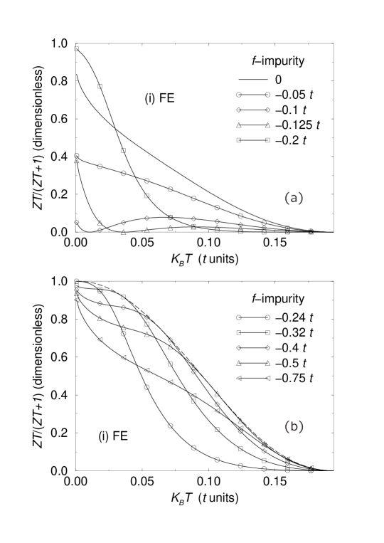
To study the behavior of as the -impurity varies, we take a series of “snapshots” depicting vs for different values of in Fig. 7. Figure 7(a) focuses on , in a range between 0 and -0.2. We see that, as is lowered from its zero value, conspicuously decreases: in this range changes sign. At -0.1 and -0.125 a temperature exists at which : these temperatures correspond to the zero of in Fig. 6 (left panel). At -0.2, however, begins to rise. In Fig. 7(b) we analyze the “high-value region” of . At -0.24 the curve is quite depressed around 0.1 (room temperature with the usual numerical parameters), but it acquires giant values around , close to the theoretical upper bound 1. Moreover, the shape of the curve is very different from the typical pattern of the -impurity layer: in this latter case the curve is convex around , while in the present situation is concave, i.e. if one slightly departs from will still be very high. This approximate flatness of the curve suggests that a stable low-temperature working point should exist for a junction-based device. As is furtherly decreased, shows a concave “shoulder” which is shifted towards higher temperatures. This feature implies that, once we fix a temperature, it is possible to find an optimal value of maximizing the figure of merit. This locus of optimal working points is manifestly given by the envelope curve for the “shoulders” (dashed line). The behavior of as rises from zero () is similar, but the sequence is inverted with respect to the case we have just examined: this time first dramatically increases, and then rapidly drops to low values.
Figure 8 shows the maximum values of vs that can be reached with a suitable -impurity energy . Up (down) triangles indicate positive (negative) optimal energies . Analogous results for NB (dot-dashed lines) are shown. The curves correspond to the loci of the - space like the envelope curve of Fig. 7(b). From Fig. 8 we can derive the absolute maxima of . Our results are that, at room temperature ( 0.1, with the usual numerical parameters) 1 for FE and 1.6 for NB, at 150 K is 6 in both cases, at 100 K is 13, and at 40 K is 100.
These extremly high values suggest the possibility of engineering a periodic lattice of -layers made of metal and strongly correlated semiconductor to create an efficient thermoelectric device. Borrowing an intuition of Refs. thermionic, and moyzhes, , the bias applied to the superlattice should be such that the electronic transport occurs perpendicular to interfaces. The thickness of each layer should be comparable to the electronic mean free path, and large enough to prohibit electrons from tunnelling. In this regime the electronic motion within each layer is ballistic, and the interfaces can be considered as the only scattering mechanisms. Mahan and Woodsthermionic call thermionic a similar device with an ordinary semiconductor replacing the strongly correlated one, because the electronic motion is ballistic and the expression for the current is the Richardson’s equation. However, here the situation is different, because the transmission coefficient has such a sharp variation with energy that the current has a more complex form than the Richardson’s expression and it requires a full analysis of the role of the interface in transport. The idea here is to grow a -atom overlayer at with optimal -level energy depending on the working temperature of the device. In addition, we find that the magnitude of thermal conductance changes only slightly with . The -layer of rare-earth atoms could also act like an additional source of strong scattering for phonons, thus lowering the lattice thermal conductance.physicstoday Therefore the junction is a promising candidate as a thermoelectric device.
IV.4 Effects of the surface on the lattice structure
We briefly comment on the influence which the interface has on the ideal lattice structure. We consider the narrow band semiconductor NB. If the effect of the surface at is to locally shorten the lattice constant , this will certainly change the hybridization parameter between the -site at and the -site at . Presumably will be increased. Modifying nothing but with respect to the clean interface case, we find that is only slightly affected by this relaxation effect. In particular, to change up to 10% almost rigidly shifts over the whole temperature range by approximately 10 – 15 %. From a check of the transmission coefficient, we find that this surface effect represents only a minor perturbation to the electronic transport across the junction.
V Conclusions
We have made a qualitative theoretical study of the possibility that a junction of metal and FE or NB (as opposed to bulk materials or to a junction metal/SC) produces high thermopower. This is possible if a -layer of suitable rare-earth impurity atoms substitutes the original layer at the interface. The localized character of the impurity -orbital has a strong effect on the transmission of carriers across the junction. The figure of merit attained is very high, especially at low temperatures. A realistic device is proposed which exploits the thermoelectric potentialities of the junction.
Acknowledgements.
This work is supported by the NSF contract DMR 0099572, MIUR-FIRB “Quantum phases of ultra-low electron density semiconductor heterostructures”, and MIUR Progetto Giovani Ricercatori. The authors thank Professors D. Chemla, M. L. Cohen and S. G. Louie for the hospitality of University of California Berkeley, where this work was initiated. M. R. is grateful to Professors Franca Manghi and Elisa Molinari for all the help given. L. J. S. thanks J. E. Hirsch for helpful discussions and the Miller Institute for support. Con il contributo del Ministero degli Affari Esteri, Direzione Generale per la Promozione e la Cooperazione Culturale.Appendix A Current operator
In this appendix we derive the form of the density current operator for the effective Hamiltonian of Eq. (18) (or ). This is a key quantity in computing the transport properties of the junction.
One way to find is to exploit the gauge invariance of the hamiltonian (18). In the presence of an oscillating, uniform electric field along ( is the time and is the frequency), one must add to a term representing the coupling to the applied field. One thus introduces the vector potential such that , where is the speed of light. The gauge transformation
| (94) |
removes the coupling to the vector potential preserving the gauge invariance of ; if we apply the transformation (94) to we obtain a new Hamiltonian which must be given, expanding to first order in , by
| (95) |
Equation (95) permits to identify , whose expression is
| (96) |
| (97) |
| (98) | |||||
| (99) |
Here is the electric current operator at atomic site (in one dimension the current coincides with its density). If the transport across the junction is stationary, at each site the current must be conserved; thus, to identify the density current associated with each quasi-particle excitation, we can calculate the operator at some suitable atomic site where its expression is simpler: this is used in Sec. III. For is a simple tight-binding Hamiltonian, and the formula for becomes, replacing and operators in (97) with operators:
| (100) |
It turns out that the constant third term on the right-hand side of Eq. (100) is always zero, hence it is easy to identify the electric current and associated with each electron or hole excitation, respectively:
| (101) | |||||
| (102) |
| (103) | |||||
The particle current density for electrons is given by
| (104) |
and for holes by
| (105) |
The picture consistent with these results is that [or ] represents the two-component electron (hole) wavefunction of the elementary excitation, and () is its probability current density. Indeed, equations (102-103) can be derived also from the continuity equation of wavefunctions, if one associates the electron amplitude with the charge , and the hole amplitude with . To obtain the continuity equation, one has to multiply the time-dependent BdG equation (46) [(47)] by [], and the complex conjugate of (46) [(47)] by [], and finally subtract one term from the other.
In an analogous way we can also write the expression of the current for . If and are real, one obtains:
| (106) |
| (107) |
References
- (1) Gerald Mahan, Brian Sales and Jeff Sharp, Phys. Today 50 (3), 42 (1997). For a review see G. D. Mahan, “Good Thermoelectrics”, in Solid State Physics 51, ed. H. Ehrenreich and F. Spaepen, Academic Press, (1998), p. 81.
- (2) A value of at room temperature has been recently reported for -type Bi2Te3/Sb2Te3 superlattice devices, see R. Venkatasubramanian, E. Siivola, T. Colpitts, and B. O’Quinn, Nature (London) 413, 597 (2001).
- (3) A preliminary report of the results of this work was given in Massimo Rontani and L. J. Sham, Appl. Phys. Lett. 77, 3033 (2000).
- (4) See B. C. Sales, D. Mandrus, and R. K. Williams, Science 272, 1325 (1996), and references therein.
- (5) G. D. Mahan and J. O. Sofo, Proc. Natl. Acad. Sci. USA, 93, 7436 (1996).
- (6) G. D. Mahan, J. Appl. Phys. 65, 1578 (1989); J. O. Sofo and G. D. Mahan, Phys. Rev. B 49, 4565 (1994).
- (7) Wenjin Mao and Kevin S. Bedell, Phys. Rev. B 59, R15590 (1999).
- (8) L. D. Hicks and M. S. Dresselhaus, Phys. Rev. B 47, 12727 (1993); L. D. Hicks, T. C. Harman, and M. S. Dresselhaus, Appl. Phys. Lett. 63, 3230 (1993).
- (9) J. O. Sofo and G. D. Mahan, Appl. Phys. Lett. 65, 2690 (1994).
- (10) L. D. Hicks, T. C. Harman, X. Sun, and M. S. Dresselhaus, Phys. Rev. B 53, R10493 (1996); T. C. Harman, D. L. Spears, and M. P. Walsh, J. Electronic Materials, 28, L1 (1999).
- (11) T. Yao, Appl. Phys. Lett. 51, 1798 (1987); S. M. Lee, D. G. Cahill, and R. Ventakasubramanian, Appl. Phys. Lett. 70, 2957 (1997); G. Chen and M. Neagu, Appl. Phys. Lett. 71, 2761 (1997); P. Hyldgaard and G. D. Mahan, Phys. Rev. B 56, 10754 (1997); G. Chen, Phys. Rev. B 57, 14958 (1998); M. V. Simkin and G. D. Mahan, Phys. Rev. Lett. 84, 927 (2000).
- (12) M. Nahum, T. M. Eiles, and John M. Martinis, Appl. Phys. Lett. 65, 3123 (1994).
- (13) H. L. Edwards, Q. Niu, G. A. Georgakis, and A. L. de Lozanne, Phys. Rev. B 52, 5714 (1995).
- (14) G. D. Mahan and L. M. Woods, Phys. Rev. Lett. 80, 4016 (1998); G. D. Mahan, J. O. Sofo, and M. Bartkowiak, J. Appl. Phys. 83, 4683 (1998).
- (15) B. Moyzhes and V. Nemchinsky, Appl. Phys. Lett. 73, 1895 (1998).
- (16) Gao Min and D. M. Rowe, J. Phys. D: Appl. Phys. 32, L1, L26 (1999).
- (17) F. J. Blatt, P. A. Schroeder, C. L. Foiles, and D. Greig, Thermoelectric Power of Metals, Plenum, New York, (1976); G. D. Mahan, IEEE Proceedings of the 16th International Conference on Thermoelectrics, 21 (1997), and references therein; Phys. Rev. B 56, 11833 (1997).
- (18) G. Aeppli and Z. Fisk, Comments Cond. Mat. Phys. 16, 155 (1992).
- (19) Piers Coleman, Phys. Rev. B 29, 3035 (1984); A. J. Millis and P. A. Lee, Phys. Rev. B 35, 3394 (1987).
- (20) Ji-Min Duan, Daniel P. Arovas, and L. J. Sham, Phys. Rev. Lett. 79, 2097 (1997).
- (21) B. C. Sales, E. C. Jones, B. C. Chakoumakos, J. A. Fernandez-Baca, H. E. Harmon, J. W. Sharp, and E. H. Volckmann, Phys. Rev. B 50, 8207 (1994).
- (22) C. D. W. Jones, K. A. Regan, and F. J. DiSalvo, Phys. Rev. B 58, 16057 (1998).
- (23) T. Portengen, Th. Östreich, and L. J. Sham, Phys. Rev. Lett. 76, 3384 (1996); Phys. Rev. B 54, 17452 (1996).
- (24) L. M. Falicov and J. C. Kimball, Phys. Rev. Lett. 22, 997 (1969); R. Ramirez, L. M. Falicov, and J. C. Kimball, Phys. Rev. B 2, 3383 (1970).
- (25) G. D. Mahan and H. B. Lyon, Jr., J. Appl. Phys. 76, 1899 (1994).
- (26) D. A. Broido and T. L. Reinecke, Appl. Phys. Lett. 67, 100, 1170 (1995); Phys. Rev. B 51, 13797 (1995).
- (27) P. J. Lin-Chung and T. L. Reinecke, Phys. Rev. B 51, 13244 (1995); David J. Bergman and Leonid G. Fel, J. Appl. Phys. 85, 8205 (1999).
- (28) M. M. Leivo, J. P. Pekola, and D. V. Averin, Appl. Phys. Lett. 68, 1996 (1996); A. J. Manninen, M. M. Leivo, and J. P. Pekola, Appl. Phys. Lett. 70, 1885 (1997).
- (29) A. Bardas and D. Averin, Phys. Rev. B 52, 12873 (1995).
- (30) J. E. Hirsch, Phys. Rev. B 58, 8727 (1998).
- (31) P. G. de Gennes, Superconductivity in Metals and Alloys, W. A. Benjamin, New York (1966), chap. 5.
- (32) The possibility of a charge density wave [G. Czycholl, Phys. Rev. B 59, 2642 (1999)] is removed either by introducing the spin degrees of freedom to the electrons and strong on-site interaction to the -electrons or by including the Coulomb energy cost of the charge density wave.
- (33) This is a usual assumption in the literature of the normal metal/superconductor (NS) junction: see e.g. A. F. Andreev, Soviet Physics JETP 19, 1228 (1964) [English transl. from JETP 46, 1823 (1964)], and also J. E. Hirsch, Phys. Rev. B 50, 3165 (1994) for an application within the tight-binding formalism.
- (34) When is exactly zero, the local gauge invariance of the Falicov-Kimball Hamiltonian renders the electron site occupation number classical. See J. K. Freericks and V. ZlatićFreericks and references therein. However, a small breaks the local gauge invariance and the long-range order of FE is possible.ferro The broken local gauge invariance by hopping -electrons is shown beyond mean-field approximation to lead to a rich phase diagram including the FE phase.Batista
- (35) J. K. Freericks and V. Zlatić, Phys. Rev. B 58, 322 (1998).
- (36) C. D. Batista, Phys. Rev. Lett. 89, 166403 (2002).
- (37) J. M. Ziman, Electrons and Phonons, Oxford, London (1960), chap. VII.
- (38) Here should be the total thermal conductivity: however, we compute only the electronic contribution.
- (39) Note that our definition of the thermal conductance differs from the one used by other authors [see e.g. R. J. Stoner and H. J. Maris, Phys. Rev. B 48, 16373 (1993)]. In our case []=W/K, in the former case []=W/(K m2).
- (40) G. E. Blonder, M. Tinkham, and T. M. Klapwijk, Phys. Rev. B 25, 4515 (1982).
- (41) C. Sanchez-Castro, K. S. Bedell, and B. R. Cooper, Phys. Rev. B 47, 6879 (1993).