Andreev reflection and enhanced subgap conductance in NbN/Au/InGaAs-InP junctions
Abstract
We report on the fabrication of highly transparent superconductor/normal metal/two-dimensional electron gas junctions formed by a superconducting NbN electrode, a thin (10nm) Au interlayer, and a two-dimensional electron gas in a InGaAs/InP heterostructure. High junction transparency has been achieved by exploiting of a newly developed process of Au/NbN evaporation and rapid annealing at 400∘C. This allowed us to observe for the first time a decrease in the differential resistance with pronounced double-dip structure within the superconducting energy gap in superconductor-2DEG proximity systems. The effect of a magnetic field perpendicular to the plane of the 2DEG on the differential resistance of the interface was studied. It has been found that the reduced subgap resistance remains in high magnetic fields. Zero-field data are analyzed within the previously established quasiclassical model for the proximity effect.
pacs:
74.80.Fp, 73.23.-bI Introduction
The study of hybrid systems consisting of superconductors (S) in contact with a two-dimensional electron gas (2DEG) has attracted considerable interest in recent years. Various new effects arising due to the Andreev reflection at the S/2DEG interface were studied in such systems, both theoretically and experimentally Neurohr96 ; Takagaki98 ; Asano00 ; Asano00a ; Chtchelkatchev01 ; Hoppe00 ; Zuelicke01 ; Tkachov03 ; Zhou98 ; Moore99 ; Uhlisch00 ; Takayanagi02 . By taking phase-coherent Andreev reflection into account, the oscillations in the conductance of a S/2DEG junction in magnetic field have been predicted which are based on an Aharonov-Bohm-type interference effect Takagaki98 ; Asano00 ; Asano00a ; Chtchelkatchev01 . The current transport across the S/2DEG interface in the quantum Hall effect regime was investigated by Hoppe, Zülicke and Schön Hoppe00 ; Zuelicke01 . They could show that bound states are formed at the S/2DEG interface which are the coherent superposition of electron and hole edge excitations Hoppe00 . Very recently, the magneto-tunneling spectrum and the thermal conductance have been studied in a superconductor/quasi-one-dimensional semiconductor structure Tkachov03 . The transport across a superconductor/semiconductor interface in the Hall geometry was discussed in Takagaki98 ; Zhou98 . In Zhou98 , it is predicted that the Hall voltage is significantly suppressed near the interface compared to its normal metal value.
Experimental observation of these new phenomena is a challenging problem because in most cases the high probability of Andreev reflection at the interface is essential. Since Andreev reflection is a two-particle process Andreev64 , it is strongly affected by the transmissivity at the S/2DEG interface. Therefore, a serious effort has to be made to achieve a high junction transparency in order to access the novel transport regimes of interest. Recently, Takayanagi et al. Takayanagi02 reported the succesful preparation of good ohmic contacts between NbN/AuGeNi electrodes and a 2DEG in an AlGaAs/GaAs heterostructure.
In this work, we report on the fabrication of highly transparent superconductor/2DEG junctions formed by superconducting NbN electrodes and a 2DEG in a InGaAs/InP heterostructure. High junction transparency has been achieved by the use of a thin (10 nm) Au interlayer between NbN and the heterostructure. This achievement allowed us to observe for the first time a decrease in the differential resistance with pronounced double-dip structure within the superconducting energy gap and to measure the dependence of this structure on the magnetic field. Previously, experiments on transparent S/2DEG junctions (in diffusive limit) revealed a peculiar non-monotonic voltage dependence of the differential resistance with a maximum at zero bias, referred to as ”reentrant” resistance Charlat96 ; VolkovAllsopp96 ; GolubovWilhelm97 ; Nazarov96 ; Belzig99 . In diffusive S/2DEG contacts with Schottky barriers, a large and narrow peak in the differential conductance of the junctions around zero bias voltage was observed Kastalsky91 ; Magnee94 ; Quirion02 . The latter effect, known as ”reflectionless tunneling”, has been studied theoretically in Refs. Zaitsev90 ; Lambert91 ; Wees92 ; Takane92 ; Beenakker92 ; VolkovKlapwijk92 ; VolkovZaitsev93 ; Volkov93 ; Hekking93 ; Beenakker94 ; MelsenBeenakker96 ; Lesovik97 ; VolkovTakayanagi97 ; Bezuglyi00 . Below we will argue that the new double-dip structure in the differential resistance detected in our measurements is related to the transport in SN-2DEG contacts in a ballistic regime Neurohr96 . Experimental data for zero magnetic field will be analyzed in our work within the quasiclassical model for the proximity effect developed in Neurohr96 ; Golubov96 .
II Experimental
Our experiments have been performed with strained InGaAs/InP heterostructures fabricated by metal organic vapor phase epitaxy (MOVPE) on a semi-insulating InP substrate. The InGaAs/InP heterostructures consist of a 400 nm thick InP buffer, a 10 nm thick (Si)-InP dopant layer (), a 20 nm thick InP spacer, a 10 nm thick In0.77Ga0.23As layer containing the 2DEG, and a 150 nm thick In0.53Ga0.47As cap. The use of InGaAs/InP heterostructures with a strained In0.77Ga0.23As layer allows one to achieve a high mobility in the 2DEG owing to a low effective electron mass of and a reduced contribution of alloy scattering. Shubnikov-de Haas and Hall effect measurements of our 2DEG structures revealed a carrier concentration of and a mobility of about 250000 cm2/Vs at 0.3 K. From these values a Fermi energy of 37 meV and a transport mean free path of 3.6 m were estimated.
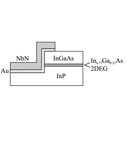
A schematic of the sample layout is shown in Fig. 1. The semiconductor mesa was defined by electron beam lithography and reactive ion etching (RIE) using CH4/H2 gas mixture. We prepared two different types of electrodes to the two-dimensional electron gas in a InGaAs/InP heterostructure. The electrodes of the first type were 100 nm thick NbN layers deposited by dc magnetron sputtering. The NbN electrodes are contacted at the mesa sidewalls to the 2DEG. Directly prior to the deposition of NbN, the semiconductor surface was cleaned by an Ar plasma, in order to remove residual atoms at the surface. At the final processing step, the geometry of the NbN electrodes were defined using a lift-off technique. The electrodes of the second type were prepared by a modified two-step process. First, after the cleaning of the surface of the etched InGaAs/InP heterostructure by Ar-plasma, a thin (10 nm) Au interlayer was deposited in situ by dc magnetron sputtering followed by the deposition of the NbN electrode. Subsequently, we employed a rapid ( 10 sec) annealing step. The temperature of annealing was 400∘C.
For the electrical characterization a three-terminal measurement scheme has been employed where a small ac current is superimposed to a dc bias current. The differential resistance is obtained by detecting the ac voltage by a lock-in amplifier. The ac excitation current was 10 nA. The measurements were performed at temperatures down to 0.3 K in a He-3 cryostat equipped with a superconducting solenoid with a magnetic field up to 10 T.
III Experimental Results
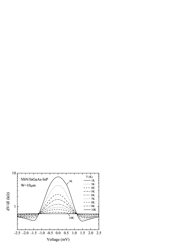
In Fig. 2, the differential resistance as a function of the bias voltage measured at different temperatures is shown for a 10 m wide NbN/2DEG interface. It is seen that at low temperatures, a pronounced resistance peak occurs at zero bias voltage, indicating a strong barrier at the NbN/2DEG interface. Measurements show that the height of the resistance peak does not depend on temperature in the low temperature range K. If the DC bias voltage approaches a value of 1.5 mV, a minimum in the differential resistance is observed. The position of this resistance minimum coincides with the superconducting energy gap determined from the critical temperature of superconductor . At voltages meV a constant differential resistance is found. With increasing the temperature the resistance peak at zero bias as well as the minima at about mV become weaker and disappear completely at temperatures above K. The interface resistances of the NbN/InGaAs-InP interfaces are relatively high due to a high barrier at the interface. In order to improve the contact characteristics, we modified the method of preparation of the S/2DEG interfaces of the structures as was discussed in the previous section. By using a thin gold interlayer, we succeeded to obtain a considerably smaller interface resistance.
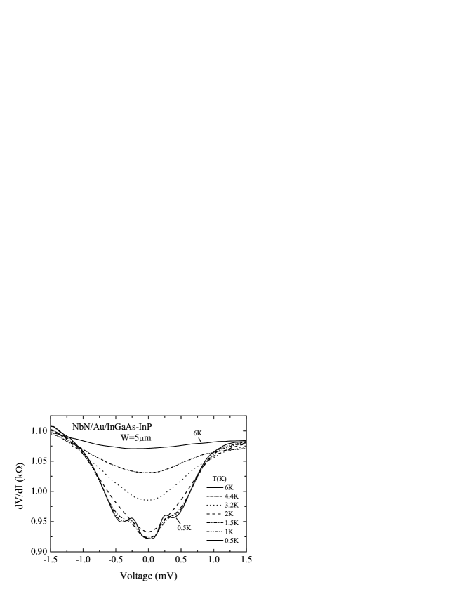
Figure 3 shows the differential resistance of a m wide NbN/Au/2DEG interface as a function of the voltage drop at different temperatures. It is seen that a decrease in the differential resistance is observed within the range of voltages mV at temperatures below 6 K. This result is a characteristic of the transport across a junction with high probability of Andreev reflection, resulting in excess current at low bias Neurohr96 ; Golubov96 . At zero dc bias voltage, the differential resistance exhibits a minimum. At 0.5 K, the zero bias resistance dip reaches a value of about 15 % of the normal state resistance . At low temperatures ( K), in the voltage dependence of the differential resistance, we observed two shoulders, both symmetric in voltage. As the temperature is increased, the double dip structure in the differential resistance progressively disappears. At temperatures higher than 2 K, the feature at small voltages is suppressed and only a broad resistance dip within the range of 1 mV remains. Finally, at temperatures about 6 K almost constant differential resistance is measured. At this temperature the sample is effectively normal conductive, since the temperature is close to .
Fig. 4 demonstrates the effect of a magnetic field perpendicular to the plane of the 2DEG on the differential resistance of the NbN/Au/2DEG interface. The differential resistance is plotted versus dc bias current and is normalized to the resistance value measured at A. The measurements were performed at 0.5 K. It is seen that with increasing magnetic field the reduction of the resistance at zero bias as related to its value at A becomes smaller. The double-dip structure occurs on the scale of about several 100 mT and is still clearly seen at T. At high fields, the features are no longer well resolved, however a reduced zero-bias resistance remains even at magnetic fields of about 3 T. Note that in our samples, the onset of the Shubnikov-de Haas oscillations in the 2DEG is observed at a magnetic field of about 0.25 T. Therefore, our experiments indicate that the subgap conductance enhancement due to Andreev reflection is preserved in the regime of high quantizing magnetic fields.
IV Discussion and Comparison with Theory
Detailed interpretation of the I-V curves in magnetic field requires separate study and will be reported elsewhere. Here we shall discuss the experimental data in zero field, in order to demonstrate that the regime of highly-transparent S/2DEG interfaces was achieved in our junctions.
First we analyze the experimental data using the well-established Blonder, Tinkham, and Klapwijk (BTK) model for the current transport Blonder82 . Although the BTK model does not include effects of disorder and an intermediate non-superconducting layer at the interface Neurohr96 , it is widely applied to both ballistic and diffusive systems, in order to obtain an estimate of the junction transmissivity. In the BTK model, a potential barrier at the interface is approximated by a -function potential. A transmission coefficient in the normal state is given by where is the dimensionless parameter characterizing the potential barrier strength Blonder82 . Following Gao93 , from the drop of the differential resistance at zero bias compared to the large bias case (experimental curve at K, Fig. 3), a barrier strength for the NbN/Au/InGaAs-InP junction is obtained. The normal-state transmission coefficient calculated from -value is 0.8, which is considerably higher than the value of obtained for NbN/InGaAs-InP junctions.
Golubov et al. Neurohr96 ; Golubov96 extended the BTK model by taking into account the presence of a non-superconducting N layer at the interface. The structure therefore may be represented as an SN-2DEG junction. The S and N layers are assumed to be in the dirty limit, while the 2DEG channel is in the clean limit Neurohr96 . The N-2DEG interface is simulated in the model by the BTK -factor.
The equilibrium state of the S and N layers is described by the angle-averaged Green’s functions and , which are obtained from the Usadel equations Belzig99 . By formally introducing a complex angle with and , the Usadel equations are written as Neurohr96 :
| (1) |
where and are the normalized energy and pair potential, and is the critical temperature of the superconductor. The coherence lengths are given by where and are the diffusion coefficients in the superconductor and normal layers, respectively.
The pair potential in the superconductor is determined by the self-consistency equation
| (2) |
where are the normalized Matsubara frequencies. In the normal conductor, the pair potential is assumed to be zero. The quasiparticle density of states (DOS) in terms of the proximity angle is obtained from , where is the Fermi level DOS in the normal state.
In order to calculate the current across a junction, the solution of the Eqs. (1, 2) for the proximity effect in the dirty SN sandwich, including the influence of a clean 2DEG, has to be found. Eqs. (1, 2) must be supplemented with the two sets of boundary conditions: at the SN interface and at the 2DEG-N interface. For the SN interface the boundary conditions are given by
| (3) | |||||
| (4) |
where is a parameter characterizing the strength of the proximity effect between S and N layers and describes the effect of the SN interface transparency, is the SN interface resistance, and are the normal state resistivities. In the bulk of the superconductor, is given by where is the bulk value of the pair potential. For the N-2DEG interface, which separates the disordered N layer (of thickness ) and the clean 2DEG, the material-dependent parameters for the boundary conditions, similar to Eqs. (3, 4), are found from the estimates Neurohr96 : and , where and are the Fermi wave-vectors in the 2DEG and in the N layer, is the mean free path in the N layer, and is the barrier strength in the BTK model. The estimations show that for our NbN/Au/2DEG junctions one may set .
The complete self-consistent problem requires numerical simulations. The self-consistent solution is then used to determine the Andreev and normal reflection coefficients at the 2DEG-N interface and the current across a junction Neurohr96 ; Golubov96
| (5) | |||||
| (6) | |||||
| (7) |
where is the Fermi distribution function, is the voltage drop in the junction and is the contact width. In Eqs. (5, 6), the function is taken in the N region near the N-2DEG interface.
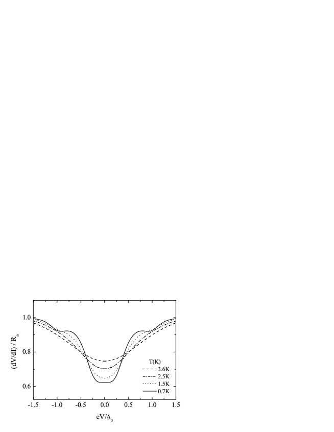
An essential feature of the model Neurohr96 ; Golubov96 is the existence of a gap in the density of states of the N layer which is in proximity to a superconductor. This leads to the characteristic two-gap structures in the energy dependence of Andreev and normal reflection coefficients and thus in the voltage dependence of the resistance Merkt97 . Fig. 5 shows the corresponding calculated curves for NbN/Au/2DEG junctions. The parameters for the calculated curves were chosen within a realistic range given by the characteristic material constants Plathner96 ; Gousev94 ; Pambianchi94 ; Nunoz00 ; Dikin02 ; Schaepers03 . As can be seen from Fig. 5 and Fig. 3, the calculated and measured curves show a rather good qualitative agreement. However, we could not find a good quantitative fit to the experimental curves. The main discrepancies are in the detailed shape and in the amplitude of variations of the differential resistance. A weaker dip in the experimental curve than calculated within the model Neurohr96 can possibly be explained by smearing due to the inhomogeneity of the junction (i.e. variation of the interface quality over the width of the junction).
We have also considered the model of diffusive contact when a disordered 2DEG channel exists between the clean 2DEG and SN electrode and a potential drop is distributed between the SN-2DEG interface and the disordered region in the 2DEG. Properties of disordered contacts have been first studied theoretically by Artemenko, Volkov, and Zaitsev Artemenko79 and later in Refs. VolkovAllsopp96 ; GolubovWilhelm97 ; Nazarov96 ; Belzig99 ; Zaitsev90 ; Lambert91 ; Wees92 ; Takane92 ; Beenakker92 ; VolkovKlapwijk92 ; VolkovZaitsev93 ; Volkov93 ; Hekking93 ; Beenakker94 ; MelsenBeenakker96 ; Lesovik97 ; VolkovTakayanagi97 ; Bezuglyi00 . The transport measurements on the S/N structures in the diffusive limit have been carried out in Kastalsky91 ; Magnee94 ; Quirion02 and have revealed a conductance peak around zero bias voltage which arises due to an interplay between Andreev scattering and disorder-induced scattering in the normal electrode. The fitting parameters we obtained within the model of diffusive contact (in particular, large thickness of the disordered 2DEG channel ) appeared to be unrealistic. Therefore, it is less likely that the diffusive model can be applied in our case when the 2DEG is in the extreme clean limit. We believe that the observation of the two-gap like structure in the differential resistance is related to the transport between the NS bilayer and clean 2DEG through the clean constriction (the situation which was considered in Neurohr96 ; Golubov96 ).
In conclusion, we fabricated highly transparent superconductor/normal metal/two-dimensional electron gas junctions formed by a superconducting NbN electrode, a thin (10nm) Au interlayer, and a 2DEG in a InGaAs/InP heterostructure. High junction transparency has been achieved by exploiting of a newly developed process of Au/NbN evaporation and rapid annealing at 400∘C. A decrease in the differential resistance with pronounced double dip structure was observed within the superconducting energy gap in junctions investigated and its magnetic field dependence was measured. It has been found that the reduced subgap resistance remains in high magnetic fields. Experimental data in zero field are analyzed within a model based on the quasiclassical Green-function approach. The present results suggest that our novel preparation method is not only advantageous for the fabrication of highly transparent S/2DEG interfaces but it might also have important implications for S/2DEG/S Josephson junction based devices.
The authors thank U. Zülicke for fruitful discussions, A. van der Hart for performing electron beam lithography on our samples and H. Kertz for his excellent assistance during the measurements. This work was supported by the Deutsche Forschungsgemeinschaft (DFG).
References
- (1) K. Neurohr, A. A. Golubov, Th. Klocke, J. Kaufmann, Th. Schäpers, J. Appenzeller, D. Uhlisch, A. V. Ustinov, M. Hollfelder, H. Lüth, and A. I. Braginski, Phys. Rev. B 54, 17018 (1996).
- (2) Y. Takagaki, Phys. Rev. B 57, 4009 (1998).
- (3) Y. Asano, Phys. Rev. B 61, 1732 (2000).
- (4) Y. Asano and T. Yuito, Phys. Rev. B 62, 7477 (2000).
- (5) N. M. Chtchelkatchev Pis. Zh. Eksp. Teor. Fiz. 73, 100 (2001) [JETP Lett. 73, 94 (2001)].
- (6) H. Hoppe, U. Zülicke, and G. Schön, Phys. Rev. Lett. 84, 1804 (2000).
- (7) U. Zülicke, H. Hoppe, and G. Schön, Physica B 298, 453-456 (2001).
- (8) G. Tkachov and V. I. Fal’ko, Phys. Rev. B 69, 092503 (2004).
- (9) F. Zhou and B. Spivak, Phys. Rev. Lett. 80, 3847 (1998).
- (10) T. D. Moore and D. A Williams, Phys. Rev. B 59, 7308 (1999).
- (11) D. Uhlisch, S. G. Lachenmann, Th. Schäpers, A. I. Braginski, H. Lüth, J. Appenzeller, A. A. Golubov, and A. V. Ustinov, Phys. Rev. B 61, 12463 (2000).
- (12) H. Takayanagi, T. Akazaki, M. Kawamura, Y. Harada, J. Nitta, Physica E 12, 922 (2002).
- (13) A. F. Andreev, Sov. Phys. JETP 19, 1228 (1964).
- (14) The reentrance effect first demonstrated in [P. Charlat, H. Courtois, Ph. Gandit, D. Mailly, A. F. Volkov, and B. Pannetier, Phys. Rev. Lett. 77, 4950 (1996)] is observed in a variety of diffusive S-N systems including highly transparent interfaces between a supercoductor and a normal metal [V. T. Petrashov, R. Sh. Shaikhaidarov, P. Delsing, and T. Claeson, JETP Lett. 67, 513 (1998) ; H. Courtois, P. Gandit, B. Pannetier, and D. Mailly, Superlattices and Microstructures 25, 721 (1999)] and transparent S/2DEG interfaces [S. G. Lachenmann, I. Friedrich, A. Förster, D. Uhlisch, and A. A. Golubov, Phys. Rev. B 56, 14108 (1997)].
- (15) A. F. Volkov, N. Allsopp, and C. J. Lambert, J. Phys. Cond. Mat. 8, L45 (1996).
- (16) A. A. Golubov, F. K. Wilhelm and A. D. Zaikin, Phys. Rev. B 55, 1123 (1997).
- (17) Yu. V. Nazarov and T. H. Stoof, Phys. Rev. Lett. 76, 823 (1996).
- (18) W. Belzig, F. K. Wilheln, C. Bruder, G. Schön, and A. D. Zaikin, Superlattices and Microstructures, 25, 1251 (1999).
- (19) A. Kastalsky, A. W. Kleinsasser, L. H. Greene, R. Bhat, F. P. Milliken, and J. P. Harbison, Phys. Rev. Lett. 67, 3026 (1991).
- (20) P. H. C. Magnee, N. van der Post, P. H. M. Kooistra, B. J. van Wees, and T. M. Klapwijk, Phys. Rev. B 50, 4594 (1994).
- (21) D. Quirion, C. Hoffmann, F. Lefloch, and M. Sanquer, Phys. Rev. B 65, 100508 (2002) (and references therein).
- (22) A. V. Zaitsev, Sov. Phys. JETP Lett. 51, 41 (1990).
- (23) C. J. Lambert, J. Phys.: Condens. Matter 3, 6579 (1991).
- (24) B. J. van Wees, P. de Vries, P. Magn e, and T. M. Klapwijk, Phys. Rev. Lett. 69, 510 (1992).
- (25) Y. Takane and H. Ebisawa, J. Phys. Soc. Japan 61, 2858 (1992).
- (26) C. W. J. Beenakker, Phys. Rev. B 46, 12841 (1992).
- (27) A. F. Volkov and T. M. Klapwijk, Phys. Lett. A 168, 217 (1992).
- (28) A. F. Volkov, A. V. Zaitsev, and T. M. Klapwijk, Physica C 210, 21 (1993).
- (29) A. F. Volkov, Phys. Lett. A 174, 144 (1993); Physica B 203, 267 (1994).
- (30) F. W. J. Hekking and Yu. V. Nazarov, Phys. Rev. Lett. 71, 1625 (1993).
- (31) C. W. J. Beenakker, B. Rejaei, and J.A. Melsen, Phys. Rev. Lett. 72, 2470 (1994).
- (32) J. A. Melsen, P. W. Brouwer, K. M. Frahm, and C. W. J. Beenakker, Europhys. Lett. 35, 7 (1996).
- (33) G. B. Lesovik, A. L. Fauchere, and G. Blatter, Phys. Rev. B 55, 3146 (1997)
- (34) A. F. Volkov and H. Takayanagi, Phys. Rev. B 56, 11184 (1997).
- (35) E. V. Bezuglyi, E. N. Bratus’, V. S. Shumeiko, G. Wendin, and H. Takayanagi, Phys. Rev. B 62, 14439 (2000).
- (36) A. A. Golubov and M. Yu. Kupriyanov, Physica C 259, 27 (1996).
- (37) G. E. Blonder, E. M. Tinkham, and T. M. Klapwijk, Phys. Rev. B 25, 4515 (1982).
- (38) J. R. Gao, J. P. Heida, B. J. van Wees, S. Bakker, and T. M. Klapwijk, Appl. Phys. Lett. 63, 334 (1993).
- (39) A proximity-induced energy gap in systems containing 2DEG has been first detected as an additional period of subharmonic gap structure oscillations in experiments on coplanar Nb/InAs/Nb Josephson junctions [A. Chrestin, T. Matsuyama, and U. Merkt, Phys. Rev. B 55, 8457 (1997)] and also in coplanar junctions involving 2DEG in an InAs/AlSb [G. Bastian, E. O. Goebel, A. B. Zorin, H. Schulze, J. Niemeyer, T. Weinmann, M. E. Bennett, and K. E. Singer, Phys. Rev. Lett. 81, 1686 (1998)]
- (40) B. Plathner, M. Schicke, T. Lehnert, K. H. Gundlach, H. Rothermel, M. Aoyagi, and S. Takada, Appl. Phys. Lett. 69, 4102 (1996).
- (41) Yu. P. Gousev, G. N.Goltsman, A. D. Semenov, and E. M. Gershenzon, J. of Appl. Phys. 75, 3695 (1994).
- (42) M. S. Pambianchi, S. M. Anlage, E. S. Hellman, E. H. Hartford, Jr, M. Bruns, and S. Y. Lee, Appl. Phys. Lett. 64, 244 (1994).
- (43) R. C. Munoz, C. Arenas, G. Kremer, and L. Moraga, J. Phys.: Condens. Matter 12, L379 (2000).
- (44) D. A. Dikin, S. Jung, and V. Chandrasekhar, Europhys. Lett. 57, 564 (2002).
- (45) Th. Schäpers, V. A. Guzenko, R. P. Müller, A. A. Golubov, A. Brinkman, G. Crecelius, A. Kaluza, and H. Lüth, Phys. Rev. B 67, 014522 (2003).
- (46) S. N. Artemenko, A. F. Volkov, and A. V. Zaitsev, Solid State Commun. 30, 771 (1979).