Nanometers-thick self-organized Fe stripes: bridging the gap between surfaces and magnetic materials
Abstract
We have fabricated -high Fe(110) stripes by self-organized (SO) growth on a slightly vicinal R(110)/Al203 surface, with R=Mo, W. Remanence, coercivity and domain patterns were observed at room temperature (RT). This contrasts with conventional SO epitaxial systems, that are superparamagnetic or even non-magnetic at RT due to their flatness. Our process should help to overcome superparamagnetism without compromise on the lateral size if SO systems are ever to be used in applications.
Arrays of epitaxial nanometer-sized (1-50 nm) magnetic structures can be grown by self-organization (SO). However such structures are superparamagnetic or even non-magnetic at room temperature (RT)Padovani et al. (1999); Hauschild et al. (1998); Gambardella et al. (2002). Indeed the energy barrier opposing spontaneous magnetization flipping roughly scales with , with the magnetic anisotropy per unit volume, and the system’s volume. 3D clusters of similar lateral size can overcome superparamagnetism at RT by increasing Sun et al. (2000). This seems not sufficient in epitaxial SOGambardella et al. (2002); Ohresser et al. (2001); Gambardella et al. (2003) because SO deposits are generally very flat, implying a very small . Therefore, beating superparamagnetism in SO deposits without compromising on the lateral density seems to imply increasing their thickness .
One way to force SO deposits to grow vertically and overcome superparamagnetism at RT is sequential depositionFruchart et al. (1999a); O.Fruchart et al. (2002). We proposed a second route, that consists in annealing a thin continuous film deposited on a vicinal surface to form an array of several atomic layers (AL)-thick stripesO.Fruchart et al. (2002); Jubert et al. (2002). In the early reports, concerning Fe/Mo(110) stripes, a stable thickness () was observed above 1-2 ALs of wetting. Yet this was not thick enough to observe static coercivity at RT, which could be obtained only for multidisperse assemblies of islands and stripes, thicker on the average. In this Letter we report the growth of thicker stripes, in the case of Fe/W(110): (). Such stripes display at RT functional features of magnetic materials: coercivity, remanence and domains, unlike conventional SO systems. The microscopic origin of the self-organization process is also unravelled.
The samples are epitaxially grown by pulsed laser deposition in a multi-chamber ultra-high vacuum setup (base pressure ), with in situ STM, RHEED and Auger spectroscopyJubert et al. (2003). Commercial sapphire wafers with a residual miscut angle are buffered with refractory metal films (Mo or W, -thick), whose surface consists of an array of atomically-flat terraces of width , separated by mono-atomic stepsJubert et al. (2002). Fe is then deposited at and annealed at , covered with 1 nm Mo for controlling the magnetic anisotropy, and finally capped by Al as a protection against oxidation. AFM (PSI Autoprobe CP) and hysteresis loops (QD MPMS-XL) were performed ex situ. Samples were then dc-demagnetized ex situ with the field applied perpendicular to the stripes. Magnetic and chemical imaging was performed under zero external field using the Spectroscopic Photo Emission- and Low Energy Electron Microscope (SPELEEM), operational at the Nanospectroscopy beamline, at the Elettra synchrotron radiation facility in Trieste, ItalyLocatelli et al. (2003). Element-selective magnetic contrast was obtained by combining energy filtered PEEM with X-ray Magnetic circular dichroism (XMCD). The circularly-polarized X-ray beam was shone on the sample at an angle of incidence of 16 ∘ and parallel to the in-plane of the sample, i.e. roughly perpendicular to the stripes. The photon energy was tuned to the Fe edge. The magnetic contrast , or XMCD asymmetry, is proportional to the projection of the magnetization along the X-ray beam direction, where for each pixel and are the intensity acquired with opposite helicity of the photon beam. The chemical contrast is given by .
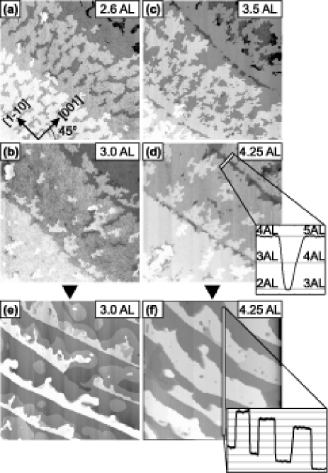
In conventional step decoration processes, the stripes have a height comparable to that of mono-atomic stepsShen et al. (1997); Hauschild et al. (1998); Gambardella et al. (2002). Figure 1 reveals the microscopic mechanism allowing the array of mono-atomic steps to serve as a template for the self-organization of stripes much thicker than the steps themselves. The frontier between the low-temperature growth mode with increasing kinetic roughnessAlbrecht et al. (1993) and the high-temperature Stranski-Krastanov growth mode with dots formationJubert et al. (2001) is . At this temperature the growth of Fe proceeds layer-by-layer on terraces, but grooves with a depth increasing with nominal Fe thickness are observed in register with the initial array of atomic steps (Figure 1b), probably resulting from stress effectsMüller et al. (2001) and the connection of interface dislocation arrays across stepsMurphy et al. (2002). Annealing Fe/W(110) films is known to yield stripes aligned along Sander et al. (1998). Here the grooves drive nucleation, yielding a self-organized array of stripes roughly aligned along for this wafer (see FIG.1a). The straighter side of the stripes is the one lying along the steps of the buffer layer (Figure 1e-f). As grooves along buried steps have been observed in other systemsCherifi et al. (2001), the self-organization process described here is expected to be of broader validity than solely for Fe/bcc(110).
In the case of Fe/W(110)/Al203 (Figure 2a, sample called Fe/W in the following) the stripes display a sharp distribution function of height, centered around independent of nominal Fe thickness, a value that is much higher than for Fe/Mo(110) (, see above). For a second sample a -thick pseudomorphic W film was deposited onto a Mo(110) buffer layer; the absence of Mo segregation towards the surface was checked with a quantitative Auger analysis. For this composite buffer layer, Fe stripes with a monodisperse thickness , again independent of nominal Fe thickness, are observed (Figure 2c, sample called Fe/W/Mo). This suggests that both the lattice parameter of the buffer layer and the interfacial energy influence the stripe thickness. The origin of this metastable thickness is under investigation. For both samples the miscut angle is , yielding a terrace width of .
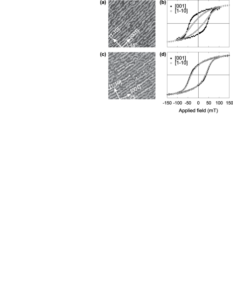
Figure 2b shows RT hysteresis loops of sample Fe/W along two in-plane directions. is a hard magnetic axis and is an easy axis, with significant remanence and a coercivity of . The coercivity at is only slightly increased to , confirming the weak effect of temperature that results from the large activation volume expected in thick stripes. This contrasts with the superparamagnetic behavior of conventional SO systems. Figure 2d shows RT hysteresis loops of sample Fe/W/Mo. This time both in-plane axes are magnetically similar, with again significant remanence and a mean coercive field of (we do not discuss the origin of anisotropy in these samples, which is a complex balance between bulk, magneto-elastic, interfaceGradmann (1993); Osgood III et al. (1995); Fruchart et al. (1999b) and shape anisotropies).
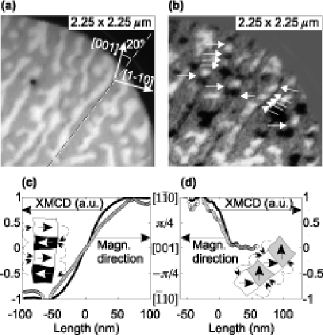
Figure 3 shows PEEM images of sample Fe/W/Mo, with a nominal thickness slightly smaller than in Figure 2c, yielding narrower and more irregular stripes (see chemical contrast on Figure 3a). In Figure 3b) light (resp. dark) areas correspond to magnetic domains pointing along (resp.) (Figure 2c), i.e. roughly perpendicular to the stripes. Grey areas correspond to domains along , i.e. roughly parallel to the stripes, or to the non-magnetic material between the stripes . These domain patterns are similar to those observed at the macroscopic scaleHubert and Schäfer (1999). They arise to satisfy both stray field flux-closure and charge-free domain walls. Depending on the local orientation of the stripes with respect to the crystallographic directions, and domain walls are observed (Figure 3c-d). We follow the usual definition of the width of a wall as the width of the linear asymptote to the plot of magnetization angle versus length. We found (Figure 3c-d) and , respectively, satisfying as expected. Note that the numerical value of is however close to the expected lateral resolution of the microscope (a few tens of nm in PEEM mode).
To conclude we have unravelled a microscopic mechanism that allows a vicinal surface to serve as a template for the self-organized growth of stripes displaying a monodisperse thickness of up to . This growth process allows one to overcome superparamagnetism without compromising on the lateral density. Thus for the first time self-organized magnetic nanostructures were observed to display at room temperature usual features of bulk materials: remanence, coercivity and domain patterns.
Acknowledgements.
We are grateful to Ph. David and V. Santonacci for their technical support, and J. Camarero, F. Scheurer and Y. Samson for preliminary magnetic measurements. This work was partly funded by Région Rhône-Alpes (Project Emergence 2001) and the French ministry of Research (ACI Nanostructures 2000).References
- Padovani et al. (1999) S. Padovani, I. Chado, F. Scheurer, and J.-P. Bucher, Phys. Rev. B. 59, 11887 (1999).
- Hauschild et al. (1998) J. Hauschild, U. Gradmann, and H. J. Elmers, Phys. Rev. B 57, R677 (1998).
- Gambardella et al. (2002) P. Gambardella, A. Dallmeyer, K. Maiti, M. C. Malagoli, W. Eberhardt, K. Kern, and C. Carbone, Nature 416, 301 (2002).
- Sun et al. (2000) S. Sun, C. B. Murray, D. Weller, L. Folks, and A. Moser, Science 287, 1989 (2000).
- Ohresser et al. (2001) P. Ohresser, N. B. Brookes, S. Padovani, F. Scheurer, and H. Bulou, Phys. Rev. B 64, 104429 (2001).
- Gambardella et al. (2003) P. Gambardella, S. Rusponi, M. Veronese, S. S. Dhesi, C. Grazioli, A. Dallmeyer, I. Cabria, R. Zeller, P. H. Dederichs, K. Kern, C. Carbone, and H. Brune, Science 300, 1130 (2003).
- Fruchart et al. (1999a) O. Fruchart, M. Klaua, J. Barthel, and J. Kirschner, Phys. Rev. Lett. 83, 2769 (1999a).
- O.Fruchart et al. (2002) O.Fruchart, P.-O. Jubert, C. Meyer, M. Klaua, J. Barthel, and J. Kirschner, J. Magn. Magn. Mater. 239, 224 (2002).
- Jubert et al. (2002) P.-O. Jubert, O. Fruchart, and C. Meyer, J. Magn. Magn. Mater. 242-245, 565 (2002).
- Jubert et al. (2003) P. O. Jubert, O. Fruchart, and C. Meyer, Surf. Sci. 522, 8 (2003).
- Locatelli et al. (2003) A. Locatelli, A. Bianco, D. Cocco, S. Cherifi, S. Heun, M. Marsi, M. Pasqualetto, and E. Bauer, J. Phys. IV-proceedings 104, 99 (2003).
- Shen et al. (1997) J. Shen, M. Klaua, P. Ohresser, H. Jenniches, J. Barthel, C. V. Mohan, and J. Kirschner, Phys. Rev. B56, 11134 (1997).
- Albrecht et al. (1993) M. Albrecht, H. Fritzsche, and U. Gradmann, Surf. Sci. 294, 1 (1993).
- Jubert et al. (2001) P.-O. Jubert, O. Fruchart, and C. Meyer, Phys. Rev. B 64, 115419 (2001).
- Müller et al. (2001) P. Müller, P. Turban, L. Lapena, and S. Andrieu, Surf. Sci. 488, 52 (2001).
- Murphy et al. (2002) S. Murphy, D. Mac Mathúna, G. Mariotto, and I. V. Shvets, Phys. Rev. B 66, 195417 (2002).
- Sander et al. (1998) D. Sander, A. Enders, C. Schmidthals, D. Reuter, and J. Kirschner, Surf. Sci. 402-404, 351 (1998).
- Cherifi et al. (2001) S. Cherifi, C. Boeglin, S. Stanescu, J. P. Deville, C. Mocuta, H. Magnan, P. Le Fèvre, P. Ohresser, and N. B. Brookes, Phys. Rev. B 64, 184405 (2001).
- Gradmann (1993) U. Gradmann, in Handbook of magnetic materials, edited by K. H. J. Buschow (Elsevier Science Publishers B. V., North Holland, 1993), vol. 7, chap. 1, pp. 1–96.
- Osgood III et al. (1995) R. M. Osgood III, R. L. White, and B. M. Clemens, Mat. Res. Soc. Symp. Proc. 384 (1995).
- Fruchart et al. (1999b) O. Fruchart, J.-P. Nozières, and D. Givord, J. Magn. Magn. Mater. 207, 158 (1999b).
- Hubert and Schäfer (1999) A. Hubert and R. Schäfer, Magnetic domains. The analysis of magnetic microstructures (Springer, Berlin, 1999).