Enhancement of the Curie temperature in GaMnAs/InGaMnAs superlattices
Abstract
We report on an enhancement of the Curie temperature in GaMnAs/InGaMnAs superlattices grown by low-temperature molecular beam epitaxy, which is due to thin InGaMnAs or InGaAs films embedded into the GaMnAs layers. The pronounced increase of the Curie temperature is strongly correlated to the In concentration in the embedded layers. Curie temperatures up to 110 K are observed in such structures compared to 60 K in GaMnAs single layers grown under the same conditions. A further increase in TC up to 130 K can be achieved using post-growth annealing at temperatures near the growth temperature. Pronounced thickness fringes in the high resolution X-ray diffraction spectra indicate good crystalline quality and sharp interfaces in the structures.
pacs:
75.50.Pp; 71.55.Eq; 81.15.Hi; 75.70.Cn; 73.21.CdDeveloping ferromagnetic semiconductors with Curie temperatures near room temperature or beyond is of major interest for future spintronic devices. One material under intense investigation in recent years is the diluted magnetic semiconductor Ga1-xMnxAs which can be made ferromagnetic at present with Curie temperatures up to 110 KMatsukuratransport in as-grown samples and up to 150 KKuannealing in annealed samples. GaMnAs is fabricated by low-temperature (LT) molecular beam epitaxy (MBE) with growth temperatures of around 250∘C, and therefore, a lot of defects are incorporated into the lattice. Different defect species like As antisites, AsGa, or As interstitials, AsI, as well as Mn interstitials, MnI, are discussed in the literature,Potashnik -Blinowski_interstitials having one aspect in common: They are all acting as donors and are therefore compensating the Mn acceptors in GaMnAs. Hence, the defect structure influences strongly the electrical and, consequently, the magnetic properties of this material system, since the ferromagnetic coupling in GaMnAs is suggested to be due to an indirect exchange interaction between the magnetic moments of Mn++-ions mediated by holes.DietlScience287zenermodell So, one possible way to increase the Curie temperature TC in GaMnAs is to increase the hole concentration, e.g., by reducing the defect density in the material by post-growth annealing at temperatures near or even below the growth temperature.Kuannealing ,Foxon Another possibility to change the magnetic properties is to control the defect structure of the material even during growth.Tanaka_epitaxial -Campion_epitaxial
Here, we report on the increase of TC of GaMnAs due to strained (InyGa1-y)1-xMnxAs or InyGa1-yAs layers embedded into the magnetically active GaMnAs layers.
All samples studied were grown on epiready semi-insulating GaAs(001) substrates in a Riber 32 MBE system. To provide As4, an As cracker cell was used in the non-cracking mode. To supply Ga and In fluxes, conventional Knudsen cells were used, whereas a Hot-Lip cell was used for Mn. The growth procedure of the GaMnAs/InGaMnAs superlattices was as follows: First, a 100 nm thick GaAs buffer layer was grown at a substrate temperature of TS = 585∘C (standard GaAs growth conditions). Then the sample was cooled down during a growth break to the growth temperature of TS = 230∘C. The growth was continued by a 20 nm thick Ga1-xMnxAs layer followed by a 3-6 nm thick (InyGa1-y)1-xMnxAs layer. This LT procedure was repeated 15 times. Finally, the structure was capped by an additional 20 nm thick Ga1-xMnxAs layer. The In content in the InGaMnAs films was varied from sample to sample between zero and 50%. Mn-flux was kept constant during the whole LT-growth and corresponded to a Mn content of = 0.058 in the Ga1-xMnxAs layers. In the (InyGa1-y)1-xMnxAs layers it was somewhat less, depending on the In content in the sample. The same growth procedure was used to grow the GaMnAs/InyGa1-yAs superlattices except the missing Mn in the embedded layers. The growth was monitored in situ by reflection high energy electron diffraction (RHEED). The RHEED pattern showed (1 2) reconstruction during the growth of the whole LT part of the structure and no evidence of a second phase on the surface (i.e. MnAs-clusters) was observed. Details of the growth of GaMnAs single layers is also described elsewhere.Koeder_gradient Annealing experiments were performed in air using a LINKAM THMS 600 heating chamber. The annealing temperature was chosen to be 250∘C, and the annealing time was 30 min. Details of the annealing experiments are described elsewhere.wolfgang_annealing
For all superlattices we performed high resolution X-ray diffraction (HRXRD) measurements. As seen for example in Fig. 1, the --scans indicate good crystalline quality and sharp interfaces between the GaMnAs and the InGaMnAs or InGaAs layers. Up to ten superlattice peaks can clearly be resolved, and even between the peaks pronounced thickness fringes are observed (see inset Fig. 1). From the superlattice fringes, the period of the superlattices can be caluclated. In the particular example, the 23.6 nm derived from HRXRD are in good agreement to what we expect from the growth rates. Finally, the sharp symmetrical peaks indicate a fully strained structure.

superlattice. The inset shows pronounced thickness fringes between the zero order peak and the second order peak.
A series of samples containing GaMnAs/InGaMnAs superlattices were grown with varying In content from 0% In (single layer) up to 50% In. To extract the Curie temperature of the samples superconducting quantum interference device (SQUID) magnetization measurements were performed as a function of temperature (accuracy 5 K) in a small in-plane applied magnetic field (50 Oe (110)). As can be seen in Fig 2, TC is continously increasing with increasing In content (filled squares) from 60 K in the GaMnAs single layer up to 110 K in the as-grown structure containing 50% In.
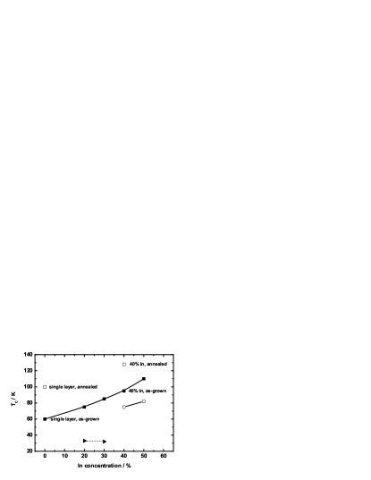
Curie temperature as a function of In-content in GaMnAs/InGaMnAs superlattices. Filled squares: as-grown GaMnAs/InGaMnAs, open squares: annealed GaMnAs/InGaMnAs, open circles: as-grown GaMnAs/InGaAs, filled triangles: as-grown LT-GaAs/InGaMnAs. The lines are to guide the eye.
In order to further analyze this effect, several reference samples were grown under the same growth conditions: First, two LT-GaAs/InGaMnAs superlattices containing 20 and 30% In, in order to clarify whether the higher Curie temperature stems from the GaMnAs or the InGaMnAs layers. These two samples, in Fig. 2 marked by filled triangles, show much lower Curie temperatures of around 30K. Therefore, the InGaMnAs films alone cannot be responsible for the high Curie temperatures in the superlattices. Second, two GaMnAs/InGaAs superlattices containing 40 and 50% In (open circles in Fig. 2). These two samples show enhanced Curie temperatures of 70 and 80 K, respectively, even though there is no Mn in the InGaAs. The reason for the differences in TC, measured for the superlattices with and without Mn in the InGaMnAs layer, is not yet known.
Obviously, the high Curie temperatures of the superlattices are due to an enhancement of TC in the GaMnAs layers by incorporating strained In-containing layers.
A further increase in TC was observed upon annealing the samples 30 min at 250∘C, which is near the growth temperature. Finally, a Curie temperature of 100 K was observed for the annealed GaMnAs single layer and 130 K for the annealed superlattice containing 40% In (open squares in Fig. 2).
The hole concentrations of heavily doped GaMnAs layers can be estimated by a careful inspection of the coupled plasmon-LO-phonon modes, observed in Raman spectroscopy. Details of this method are described elsewhere.LimmerRaman In Fig. 3, the Raman spectra recorded from the GaMnAs single layer (sample B313) and from the GaMnAs/InGaMnAs superlattice with 40% In (sample B315) before and after annealing are depicted for comparison. All four spectra exhibit a broad Raman line, located near the frequency of the GaAs TO phonon, which arises from the coupled mode. With increasing hole concentration this line is known to shift from the frequency of the LO phonon to that of the TO phonon. Therefore, the Raman spectra reveal two features: First, an increase of the hole concentration upon annealing in both samples, and second, a significant enhancement of the hole concentration in the GaMnAs region of the superlattices compared to the GaMnAs single layer.

Raman spectra recorded from a GaMnAs single layer (B313)and a GaMnAs/InGaMnAs superlattice with 40% In (B315) before and after annealing.
This agrees very well with the observed increase in TC. Figure 4 shows the SQUID magnetization curves of the superlattice in Fig. 3 (sample B315) before and after annealing. The increase in Curie temperature and also in saturation magnetization due to annealing can clearly be seen.
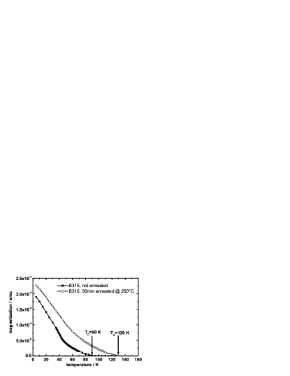
SQUID magnetization curves of a superlattice containing 40% In in the embedded layer before and after annealing at 250∘C.
At present, the underlying mechanism of the drastic enhancement of TC in the GaMnAs/InGaMnAs heterostrucures is still unclear. However, we suggest that the incorporation of strained InGaMnAs or InGaAs films into GaMnAs leads to a reduction of the density of compensating defects, resulting in a higher hole density, and thus, in a higher Curie temperature than in GaMnAs single layers. This assumption is in agreement with the Raman data which revealed an increase of the hole density in the GaMnAs barrier layers of the superlattices compared to the GaMnAs single layer. From recent publicationsYuinterstitials ,Blinowski_interstitials it is known, that the defects, which are most likely responsible for carrier compensation in GaMnAs, are the Mn atoms on interstitial sites, and LT-annealing can reduce their density. Edmonds et al.Edmonds_annealing_interstitials demonstrated that out-diffusion of MnI towards the surface takes place during annealing of GaMnAs single layers. In GaMnAs/InGaMnAs superlattices, the In-containing layers and/or interfaces can act as sinks for point defects like MnI and AsI during the growth. Most likely diffusion of MnI towards the heterointerfaces is responsible for the increase in carrier density and, consequently, TC. Since in our superlattices a further enhancement of TC can be achieved by post-growth annealing, too, a considerable amount of MnI ions seems to be still present in the as-grown superlattices. In contrast to GaAs/GaMnAs interfaces, which have been shown to prevent removal of MnI during annealing,Kuannealing the embedded InGaMnAs layers obviously do not have any adverse effect on the annealing process.
In summary we have shown that the Curie temperature of epitaxially grown GaMnAs layers can be increased by embedding strained InGaMnAs or InGaAs layers into the magnetically active GaMnAs. We suggest that this is due to the influence of strain on the diffusion of defects like Mn and As interstitials into the In containing embedded layers, or to the reduction of their concentration during growth as compared to GaMnAs single films. The Curie temperature can be controlled by varying the In content in the embedded layers.
The authors acknowledge the financial support by the Deutsche Forschungsgemeinschaft, DFG Wa 860/4-1.
References
- (1) F. Matsukura, H. Ohno, A. Shen, and Y. Sugawara, Phys. Rev. B 57, R2037 (1998)
- (2) K. C. Ku, S. J. Potashnik, R. F. Wang, M. J. Seong, E. Johnston-Halperin, R. C. Meyers, S. H. Chun, A. Mascarenhas, A. C. Gossard, D. D. Awschalom, P. Schiffer, and N. Samarth, Appl. Phys. Lett. 82, 2302 (2003).
- (3) S.J. Potashnik, K.C. Ku, S.H. Chun, J.J. Berry, N. Samarth, and P. Schiffer, Appl. Phys. Lett. 79, 1495 (2001).
- (4) K.M. Yu, W. Walukiewicz, T. Wojtowicz, I. Kuryliszyn, X. Liu, Y. Sasaki, and J.K. Furdyna, Phys. Rev. B 65, 201303(R) (2002).
- (5) J. Blinowski and P. Kacman, Phys. Rev. B 67, 121204 (R) (2003)
- (6) T. Dietl, H. Ohno, F. Matsukura, J. Cibert, and D. Ferrand, Science 287, 1019 (2000).
- (7) K.W. Edmonds, K.Y. Wang, R.P. Campion, A.C. Neumann, N.R.S. Farley, B.L. Gallagher, and C.T. Foxon, Appl. Phys. Lett. 81, 4991 (2002).
- (8) M. Tanaka, J. Vac. Sci. Technol. B 16(4), 2264 (1998)
- (9) A. Shen, F. Matsukura, S.P. Guo, Y. Sugawara, H. Ohno, M. Tani, H. Abe, and H.C. Liu, Journal of Crystal Growth 201/202, 679 (1999)
- (10) R. P. Campion, K. W. Edmonds, L. X. Zhao, K. Y. Wang, C. T. Foxon, B. L. Gallagher, and C. R. Staddon, Journal of Crystal Growth 247, 42 (2003)
- (11) A. Koeder, S. Frank, W. Schoch, V. Avrutin, W. Limmer, K. Thonke, R. Sauer, M. Krieger, K. Zuern, P. Ziemann, S. Brotzmann, H. Bracht, and A. Waag, Appl. Phys. Lett. 82, 3278 (2003)
- (12) W. Limmer, A. Koeder, S. Frank, M. Glunk, W. Schoch, V. Avrutin, K. Zuern, R. Sauer, and A. Waag, cond-mat 0307102, to be published in Physica E
- (13) W. Limmer, M. Glunk, S. Mascheck, A. Koeder, D. Klarer, W. Schoch, K. Thonke, R. Sauer, and A. Waag, Phys. Rev. B 66, 205209 (2002).
- (14) K.W. Edmonds, P. Boguslawski, K.Y. Wang, R.P. Campion, N.R.S. Farley, B.L. Gallagher, C.T. Foxon, M. Sawicki, T. Dietl, M.B. Nardelli, and J. Bernholc, cond-mat 0307140, (2003)