Interaction Effects at Crossings of Spin-Polarised One-Dimensional Subbands
Interaction Effects at Crossings of Spin-Polarised One-Dimensional Subbands
Abstract
We report conductance measurements of ballistic one-dimensional (1D) wires defined in GaAs/AlGaAs heterostructures in an in-plane magnetic field, . When the Zeeman energy is equal to the 1D subband energy spacing, the spin-split subband intersects , where is the index of the spin-degenerate 1D subband. At the crossing of and subbands, there is a spontaneous splitting giving rise to an additional conductance structure evolving from the plateau. With further increase in , the structure develops into a plateau and lowers to . With increasing temperature and magnetic field the structure shows characteristics of the 0.7 structure. Our results suggest that at low densities a spontaneous spin splitting occurs whenever two 1D subbands of opposite spins cross.
pacs:
71.70.-d, 72.25.Dc, 73.21.Hb, 73.23.AdStudies of ballistic transport in one dimension (1D) have shown that a spontaneous spin splitting may occur at zero magnetic field, as indicated by a conductance structure at , which drops to in an in-plane magnetic fieldThomas et al. (1996). This so-called 0.7 structure is widely reported in various types of ballistic 1D wires defined in GaAsThomas et al. (1996); Kristensen et al. (1998); Reilly et al. (2001); Cronenwett et al. (2002)and Si heterostructuresBagraev et al. (2002). In some cases, at very low electron densities a structure has been observed at at zero magnetic field which strengthened with in-plane magnetic fieldThomas et al. (2000), indicating a complete spin polarisationGold and Calmels (1996); Wang and Berggren (1996).
By studying Zeeman splitting of 1D subbands, it was shown that the 0.7 structure is accompanied by an enhancement of the Lande -value as the 1D subbands are depopulated, and the energy difference between the spin-split 1D subbands tends to a finite value at zero magnetic fieldThomas et al. (1996). The conductance plateau at , either observed in zero magnetic field or induced by Zeeman effect, rises to with increasing temperatureThomas et al. (2002). None of these characteristics can be explained within a single particle model. As the situation is dynamic, for short ballistic 1D wires, zero-field spin splitting may not be in conflict with the theorem of Lieb and MattisLieb and Mattis (1962).
The discovery of the 0.7 structure in ballistic 1D wires has stimulated much theoretical work in one-dimension, some of which focused on zero-field spin polarisationSpivak and Zhou (2000); Bruus et al. (2001); Starikov et al. (2003), spin density wave formationReimann et al. (1999), pairing of electronsFlambaum and Kuchiev (2000), singlet-triplet formationRejec et al. (2000), Kondo-like interactionsLindelof (2001); Cronenwett et al. (2002); Meir et al. (2002), and electron-phonon effectsSeelig and Matveev (2002). Experimental studiesThomas et al. (1996); Kristensen et al. (1998); Reilly et al. (2001) of the 0.7 structure have, in general, indicated that due to a spin splitting at zero magnetic field, a complex many-body state may exist in a ballistic 1D constriction. In order to further study the role of spin, a strong magnetic field is applied parallel to a quantum wire to produce large Zeeman splitting and induce crossings between spin-split 1D subbandsDaneshvar et al. (1997). In this work, we show that at the crossing of Zeeman-split 1D subbands of opposite spins and different spatial wavefunctions, a spontaneous splitting sets in, giving rise to new conductance structures exhibiting characteristics of the 0.7 structure; we call this new structure a 0.7 analogue. We have observed such 0.7 analogues in eight samples, with magnetic field applied in both in-plane directions.

Split-gate devices were defined by electron beam lithography on a Hall bar etched from a high mobility GaAs/AlxGa1-xAs heterostructure. Samples A and B used in this work have a length 0.4 m and widths 0.6 m and 0.5 m. The two-dimensional electron gas (2DEG) formed nm below the surface has a mobility of cm2/Vs and a carrier density of cm-2. Conductance measurements were performed in a dilution refrigerator using an excitation voltage of 10 V at 77 Hz. The samples were mounted with the magnetic field, , parallel to the current direction. By monitoring the Hall voltage, the out-of-plane misalignment was measured to be less than .
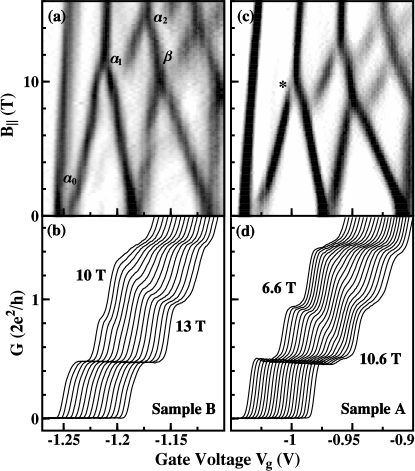
Figure 1 shows differential conductance traces, measured as a function of split-gate voltage at fixed magnetic fields, . The inset shows a schematic illustration of linear Zeeman splitting of 1D energy subbands for a parabolic potential confinement. The left trace of the main figure shows conductance plateaus quantised at and the 0.7 structure at =0. As is incremented to 15.6 T (right trace), the overall conductance characteristics undergo three major changes. These correspond to P, Q and R in Fig. 1 inset. Firstly, each spin-degenerate 1D subband splits into two, and (see P in the inset), and new conductance plateaus appear at half-integer values of . Secondly, with further increase of , the half-integer plateaus strengthen and integer plateaus weaken. When the Zeeman energy, , is equal to the subband energy spacing, , integer plateaus disappear. This happens when the split levels, for example, and converge and pass through a crossing point (see Q in the inset). Finally, with further increase of , half-integer plateaus weaken and integer plateaus reappear as the and diverge again after the crossing (see R in the inset). For example, the plateau at weakens and the plateau reappears for T. However, this is accompanied by the evolution of a weak structure from the edge of the plateau, which gradually lowers to and develops into a plateau. This resembles the evolution of the 0.7 structure to with increasing . For this reason, we call the structure at the crossing a 0.7 analogue. It may be noted that the reappearing plateau now carries the opposite spin to that before crossing. The lowest subband 1, however, does not encounter a crossing; therefore the plateau at is intact, and does not change its spin.
The evolution of conductance characteristics with the splitting of 1D subbands in can be clearly represented in a grey-scale plot of the transconductance , obtained by numerical differentiation of characteristics. Figure 2(a) shows plots of sample B as a function of and . White regions represent low transconductance (plateaus in ) and the dark thick lines correspond to high transconductance (transitions between plateaus). Each dark line splits into two as increases. This can be interpreted as the splitting of each 1D subband into two subbands of opposite spins as shown by P in the Fig. 1 inset. On the left of Fig. 2(a), for , there are two distinct dark lines at . The white region between these two dark lines represents the 0.7 structure, marked by . As the gap between the and widens with , the 0.7 structure evolves into a plateau at and the white region () in Fig.2(a) broadens. At T, dark lines corresponding to and subbands cross. After the crossing, the line shows a discontinuous shift of mV from the crossing point, marked by . This discontinuity in the dark line corresponds to the appearance of the 0.7 analogue. Figure 2(b) shows traces horizontally) in the vicinity of from a different cool-down of the sample, highlighting the evolution of the 0.7 analogue from the edge of plateau to with increasing . It is observed that the plateau, though weakening, remains visible when the 0.7 analogue evolves.
The discontinuous evolution of the right-moving dark lines (-spin subbands) can also be observed at the crossing of with lines marked by , and at the second crossing of with line, marked by . Figure 2(c) and (d) show results of sample A in a different cool-down from that of Fig.1. In addition to the splittings at the crossing of peaks as observed in sample B, in this case there is also a splitting just before the crossing of and peaks, marked by an asterisk in Fig.2(c). In one of the cool-downs, sample B also showed a weak splitting before the crossing. It is not clear whether this splitting marked by asterisk is related to , the 0.7 analogue. It may be observed that this corresponds to a slower rate of suppression of the plateau (1-subband) in sample A with as shown in Fig. 2(d), compared to sample B in Fig. 2(b).
In the following, we suggest that the main features of our observations arise from strong electron-electron interactions. To clarify this, we first describe the expected behaviour in the case of non-interacting electrons. In particular, we show that the diamagnetic shifts of the subband energies in an in-plane magnetic field have only a very limited influence on the most important features of our observations.
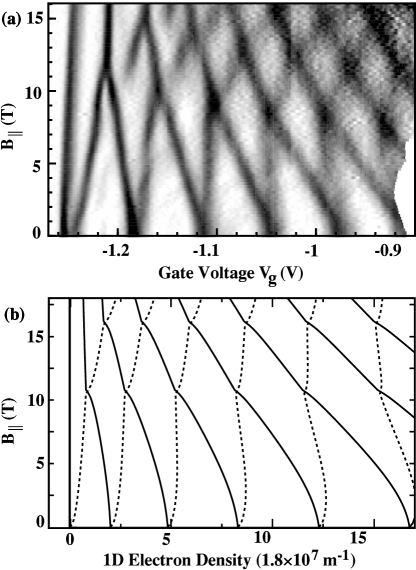
Figure 3(a) shows a greyscale plot of sample B with many occupied 1D subbands, part of which is shown in Fig. 2(a). Figure. 3(b) shows the positions of the calculated transconductance peaks as a function of electron density and for a model of non-interacting electrons in an infinite 1D wire. This model includes the diamagnetic effects with , assuming parabolic confinement in the transverse and vertical (quantum well) directions with subband spacings of 1.85 meV and 15 meV Ando (1982) respectively. A -value of 1.9 is used in this model in accordance with the value measured at low in our samples.
If one assumes that the electron density in the wire is linearly related to , then Figs. 3(a) and (b) can be compared directly. Clearly the model of non-interacting electrons accounts well for the general trends in the evolution of the transconductance peaks with and . However, the model cannot capture the appearance of discontinuities in the positions of the transconducance peaks at the crossings, , , and in Fig. 2. As we have described above, these are the regions where the conductance displays the 0.7 analogues.

Figure 4 shows the temperature dependence of the 0.7 analogue at the first crossing of 1 and 2 subbands. A defining characteristic of the 0.7 structure is its unusual temperature dependence. In addition, at low temperatures, the 0.7 structure becomes well-defined only at low electron densitiesThomas et al. (2000). For a higher 1D density, a higher temperature (typically, K in GaAs split-gate devicesThomas et al. (1996)) is required to induce the 0.7 structureKristensen et al. (1998). At high , it is well-known that the 0.7 structure develops into a plateau at ; however with an increase in , the plateau rises to Thomas et al. (2002). These trends in the temperature dependence of the 0.7 structure and plateau are also observed in the new 0.7 analogue structure at T and plateau at T. Figure 4 shows that, at T, the 0.7 analogue present just below (shown by a down-arrow) drops as rises; but at T, the plateau at (shown by an up-arrow) rises with increasing . In the inset of Fig. 4, conductance of the 0.7 analogue is plotted as a function of for a range of temperatures. This data compares well to the temperature dependence of the 0.7 structure Thomas et al. (2002), showing the crossover of as a function of at a characteristic .
Non-quantised conductance structures can be due to a change in the transmission probability caused by scattering or a many-body effect in the 1D channel. We have observed 0.7 analogues in eight samples, and they are independent of cool-downs, and occur only at the crossing of spin-split subbands of opposite spins. Due to the high reproducibility of the 0.7 analogues, a disorder-induced scattering effect can be discounted.
When two energy levels are brought together, an anticrossing may occur. However, this depends on the symmetry of the two wavefunctions. In our case, the two 1D levels that cross in have different spins and subband indices; therefore such anticrossings should be very weak. Experimentally, we do not observe anticrossings of 1D subbands, rather a gap forms abruptly after the crossing. As in the case of the 0.7 structure, we believe that the new 0.7 analogue is a consequence of strong exchange interactions. In the former case, there is a lifting of the zero-field spin-degeneracy, whereas in the latter case, the degeneracy at the crossing point is lifted. We can quantify the strength of the exchange interactions by measuring the gate voltage splitting at . From dc source-drain bias calibrationPatel et al. (1991), is measured to be 0.5 meV, which is a third of the subband spacing ( meV) at zero magnetic field.
Given the strong similarity between the 0.7 analogue and the 0.7 structure, we consider whether theories for the 0.7 structure could apply to our results. A recently proposed electron-phonon scattering mechanism for the 0.7 structureSeelig and Matveev (2002) cannot account for the observed 0.7 analogue. Consider Fig. 2(b): if the strong 0.7 analogue in these traces were the result of a conductance suppression caused by electron-phonon scattering, then one should expect at least as strong a suppression below the spin-polarised plateau; there is no such indication.
The behaviour of the 0.7 analogue does not seem to be consistent with the most simple extension of a proposed “Kondo model” for the 0.7 structureMeir et al. (2002) to the present situation – in which a Kondo impurity forms from quasibound states of the 1 and 2 levels which become degenerate at some non-zero . In this model, one would expect the 0.7 analogue feature to fall onto the plateau as is increased or decreased away from the point of degeneracy in either direction. In contrast, the 0.7 analogue evolves asymmetrically about the midpoint of the crossing. A detailed analysis within the Kondo model will be considered in a later publication.
To conclude, we have observed the crossings of spin-split 1D subbands of different spins and spatial wavefunctions in a 1D electron gas. At crossings, there is a spontaneous splitting giving rise to new conductance structures. There are no indications of anticrossings, but an energy splitting may occur whenever two 1D subbands of opposite spin are nearly degenerate. The magnetic field and temperature dependences show that the new structures strongly resemble the zero-field 0.7 structure. We believe that these 0.7 analogue structures may provide the key to a fuller understanding of the role of electron-electron interactions in ballistic 1D wires.
We thank J. T. Nicholls, D. Khmelnitskii, V. Tripathi, and C. J. B. Ford for useful discussions. This work was supported by EPSRC, UK. KJT acknowledges support from the Royal Society.
∗Current address: University of New South Wales, School of Physics, Sydney, NSW 2052, Australia.
References
- Thomas et al. (1996) K. J. Thomas, J. T. Nicholls, M. Y. Simmons, M. Pepper, D. R. Mace, and D. A. Ritchie, Phys. Rev. Lett. 77, 135 (1996).
- Kristensen et al. (1998) A. Kristensen, P. E. Lindelof, J. B. Jensen, M. Zaffalon, J. Hollingbery, S. W. Pedersen, J. Nygard, H. Bruus, S. M. Reimann, C. B. Sörenson, et al., Physica B 251, 180 (1998).
- Reilly et al. (2001) D. J. Reilly, G. R. Facer, A. S. Dzurak, B. E. Kane, R. G. Clark, P. J. Stiles, R. G. Clark, A. R. Hamilton, J. L. O’Brien, N. E. Lumpkin, et al., Phys. Rev. B 63, 121311 (2001).
- Cronenwett et al. (2002) S. M. Cronenwett, H. J. Lynch, D. Goldhaber-Gordon, L. P. Kouwenhoven, C. M. Marcus, K. Hirose, N. S. Wingreen, and V. Umansky, Phys. Rev. Lett. 88, 226805 (2002).
- Bagraev et al. (2002) N. T. Bagraev, A. D. Buravlev, L. E. Klyachkin, A. M. Malyarenko, W. Gehlhoff, V. K. Ivanov, and I. A. Shelykh, Semiconductors 36, 439 (2002).
- Thomas et al. (2000) K. J. Thomas, J. T. Nicholls, M. Pepper, W. R. Tribe, M. Y. Simmons, and D. A. Ritchie, Phys. Rev. B 61, 13365 (2000).
- Wang and Berggren (1996) C.-K. Wang and K.-F. Berggren, Phys. Rev. B 54, 14257 (1996).
- Gold and Calmels (1996) A. Gold and L. Calmels, Phil. Mag. Lett. 74, 33 (1996).
- Thomas et al. (2002) K. J. Thomas, J. T. Nicholls, M. Pepper, M. Y. Simmons, D. R. Mace, and D. A. Ritchie, Physica E 12, 708 (2002).
- Lieb and Mattis (1962) E. Lieb and D. Mattis, Phys. Rev. 125, 164 (1962).
- Spivak and Zhou (2000) B. Spivak and F. Zhou, Phys. Rev. B 61, 16730 (2000).
- Bruus et al. (2001) H. Bruus, V. V. Cheianov, and K. Flensberg, Physica E 10, 97 (2001).
- Starikov et al. (2003) A. A. Starikov, I. I. Yakimenko and K.-F. Berggren, Phys. Rev. B 67, 235319 (2003).
- Reimann et al. (1999) S. M. Reimann, M. Koskinen, and M. Manninen, Phys. Rev. B 59, 1613 (1999).
- Flambaum and Kuchiev (2000) V. V. Flambaum and M. Y. Kuchiev, Phys. Rev. B 61, 7869 (2000).
- Rejec et al. (2000) T. Rejec, A. Ramsak, and J. H. Jefferson, Phys. Rev. B 62, 12985 (2000).
- Meir et al. (2002) Y. Meir, K. Hirose, and N. S. Wingreen, Phys. Rev. Lett. 89, 196802 (2002).
- Lindelof (2001) P. E. Lindelof, Proc. SPIE 4415, 12 (2001).
- Seelig and Matveev (2002) G. Seelig and K. A. Matveev, Phys. Rev. Lett. 90, 176804(2003).
- Daneshvar et al. (1997) A. J. Daneshvar, C. J. B. Ford, A. R. Hamilton, M. Y. Simmons, M. Pepper, and D. A. Ritchie, Phys. Rev. B 55, 13409 (1997).
- Ando (1982) T. Ando, J. Phys. Soc. Jpn. 51, 3893 (1982).
- Patel et al. (1991) N. K. Patel, J. T. Nicholls, L. Martín-Moreno, M. Pepper, J. E. F. Frost, D. A. Ritchie, and G. A. C. Jones, Phys. Rev. B 44, 13549 (1991).