Fano effect of strongly interacting quantum dot in contact with superconductor
Abstract
The physics of a system consisting of an Aharonov Bohm (AB) interferometer with a single level interacting quantum dot (QD) on one of its arms, and attached to normal (N) and superconducting (S) leads is elucidated. Here the focus is directed mainly on N-AB-S junctions but the theory is capable of studying S-AB-S junctions as well. The interesting physics emerges under the conditions that both the Kondo effect in the QD and the the Fano effect are equally important. As the Fano effect becomes more dominant, the conductance of the junction is suppressed.
pacs:
PACS numbers: 74.70.Kn, 72.15.Gd, 71.10.Hf, 74.20.MnMotivation: Transport through a mesoscopic Aharonov-Bohm (AB) ring (with an interacting quantum dot (QD) situated on one of its arms) weakly attached to normal (N) metallic leads is the subject of recent intensive experimental yacoby ; weil ; Kobayashi and theoretical oreg ; gefen ; hof ; bulka ; david ; aha studies. To the above class of experiments one may also add STM measurements on a single magnetic atom adsorbed on a gold surface Madhavan . The main result of the theoretical analysis hof ; bulka indicates that in such N-AB-N junctions there is an interplay between two fundamental physical phenomena, namely, the Fano and the Kondo effects. The Fano effect is related to an interference between two electron waves one passing through the quantum dot (with a discrete level) and one travelling along the direct ’reference’ channel characterized by its continuous spectrum. It results in an asymmetric shape of the conductance as function of the applied bias (or gate) voltage. The Kondo effect is one of the simplest manifestations of many-body physics exhibiting strong correlations. It plays an important role in electron transport through quantum dots, where the role of a magnetic impurity is played here by the presence of localized electrons glazman88 ; ournca . The interplay between these two effects causes the suppression of Kondo plateau with increasing transmission through the direct channel.
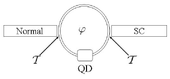
An analysis of the conductance of an AB interferometer
when one of the leads
is a normal metal and the other one is a
superconductor (S) is the subject of the present research. The
geometry of such N-AB-S junction is schematically displayed in
Fig.1.
We derive a general formula for the conductance of N-AB-S and S-AB-S
junctions.
As for the motivation, there is indeed a growing interest in these types of superconducting junctions, especially in the light of recent experiments which involve carbon nanotubes as weak linksbu ; Kas ; lin . They are characterized by relatively high Kondo temperature which helps the formation of Kondo plateau in conductance experiments. The Kondo finger-prints in such junctions is expected to survive even for cases where the superconducting gap approaches the Kondo temperature from below, that is, (see Refs.ambe ; raimondi ; us1 ).
Model Hamiltonian and the current: In the system under consideration (see Fig. 1), transport of an electron between the two-dimensional electrodes (N on the left and S on the right) is possible via two paths, either through the QD, or else through the other ’direct’ channel. The dynamics of the system is governed by the Hamiltonian
| (1) |
in which , () are the Hamiltonians of the electrons in the electrodes which depend on the electron field operators where and is the spin index,
| (2) |
Here is the BCS coupling constant and with being the chemical potential at temperature . The dot is represented by a single level Anderson impurity with energy and Hubbard repulsion . Later on we will concentrate on the Kondo regime by setting and assuming that exceeds any other energy scale except . The Nambu representation for all fermion operators ( for the lead electrons and for the QD electrons) is employed below (for example ). The dot Hamiltonian then reads,
| (3) |
where and the Pauli matrix acts in Nambu space. Assuming a symmetric junction, the tunnelling Hamiltonian from the leads to the dot is,
| (4) |
where is the tunnelling amplitude. The occurrence of direct transport channel is represented by the term between left and right leads. The gauge is chosen such that the AB flux appears only in this direct term,
| (5) |
where is the AB phase factor. Note that unlike the case of N-AB-N junctions, the phase factor is non-Abelian.
In the mean field slave boson approximation (MFA) which is employed below to handle the Kondo problem (in the limit ), the tunnelling amplitude is modified by replacing the (slave) boson operators by their mean-field values, () and the Hubbard repulsion term is dropped. This procedure imposes a constraint on the number of bosons and fermions and the Hamiltonian must now include a term which prevents double occupancy in the limit ,
| (6) |
where is the renormalized new level position which has the role of a Lagrange multiplier.
Formula for the current at one lead, say the right (supreconducting), is derived from the basic relation . It is convenient to display the result of the commutation relation in terms of Keldysh Green’s functions (GF) , namely,
| (7) |
where is the density of states in the leads (assumed to be the same in both), and the trace operation acts in Nambu and energy spaces (). Other notations are (similarly for ), where and .
Employing equation of motion method for all Keldysh GF it is possible to express the current in terms of the dot GF. We single out the current through the direct channel by writing , with,
| (8) | |||||
| (9) |
Here stands for tunneling rate through the dot, , is the dot GF, are generally nonequilibrium GF of the leads (left,right). The other two GFs include multiple scattering events and have the form,
| (10) |
Each GF (, and ) has a standard Keldysh matrix structure with elements , , , . The superscript stands for Keldysh component of the matrix product occurring in the square brackets of Eq.(7-9). The set of equations (7-10) together with the expression (7) for the current formally complete our task . They give an expression for the current through a closed AB interferometer in terms of the GF of the (strongly interacting) QD. The above formalism has been tested for the case of linear conductance with normal leads on both sides (N-AB-N junction) and the result agrees with pertinent calculations hof .
These rather general expressions are now employed for elucidating a particular case of interest, namely, the zero temperature limit of the linear conductance in N-AB-S junctions. Specifically, as in Fig. (1) the left lead is a normal metal biased with an external voltage V whose GFs are, , ; . On the other hand, the right lead is an unbiased (s-wave) superconductor with gap whose equilibrium GFs have a standard formus1 .
Mean Field Approximation and Conductance: Within the MFA the algorithm starts with calculations pertaining to a geometrically identical system albeit with noninteracting QD . Then, at the end, the replacement is executed in the conductance formula. These two quantities (the Kondo temperature and the effective renormalized position of the level) are evaluated by solving two mean field equations similar to those derived in Refs. raimondi ; us1 . At zero bias one is free to adopt the Matsubara form of these equations. The first one, , follows from the extremum requirement of the effective action over . The second one, , reflects the single occupation condition. Here
| (11) | |||
| (12) |
where . Expressions (11,12) for the dot Matsubara GF were obtained from the effective action derived from the Hamiltonian of the N-AB-S system. The self-consistence equations were solved for different values of the direct transmission parameter while the level positions are scanned over the wide range (-0.4,0.1). The parameters are tuned such that the carbon nanotubes in Kondo regime considered in reference bu can be satisfactorily regarded as an Anderson impurity. The half width of the normal electrode density of states is served as an energy unit and the tunnelling rate through the dot is fixed at . The superconducting gap is set at a value . For the majority of level positions the and thus the MFA is hence justified.
To obtain the zero bias differential conductance for the noninteracting dot, expressions for the GF are found for this case and are then directly substituted into equations (7-9). It is important to note that any element in these GF which is related to the superconductor electrode must be evaluated at energies (this is not the case for the self consistence equations). For a dot modelled by a simple resonance energy level, the formulae for the GF is(compare Eq.(11)),
Its retarded component reads then,
| (13) |
where , the coefficients of the Pauli matrices are , and . On the Fermi surface the relations , hold. Inserting these GF into equations (7-9) for the current one arrives at an expression for the zero bias conductance. After lengthy calculations the conductance is obtained and checked to be an even function of the flux, as is dictated by Onsager relations (although it is not immediately apparent, as asymmetric terms cancel).
| (14) |
Here is the background (direct) NS transmission. Introducing the quantity which is the analogous quantity (direct transmission) for the N-AB-N junctionhof then This is precisely the relation between transmission coefficients for N-BB-N and N-BB-S junctions (here BB is a “black-box” representing any non-interacting scatterer) suggested in Ref.been , using Landauer scattering matrix approach. The coefficients and in equation (14) do not depend on flux. Note, however, that the normalization factor is an even function of the flux,
The last two coefficients are and . Here the result of calculations of conductance as function of gate voltage (14) (with and zero AB phase) is shown on Fig.2. A typical Fano asymmetry form in the case is easily detected.

As was noted above, in the MFA, and appearing in the above equations should respectively be replaced by and , which, in turn, are obtained through the solutions of the self-consistence equations. The conductance of an N-AB-S junction as function of the level position is displayed in figure 3 and as a function of the flux in figure 4.


Discussion: If direct tunnelling is completely suppressed the electron trajectory passes solely through the quantum dot. This is a single channel Coulomb blockade situation for an N-QD-S junction. For level energies which satisfy pure Kondo limit, one expects Kondo behavior and Kondo plateau in the differential conductance at zero biasraimondi . We performed calculations for this range of and found such a dependence of the linear conductance. If the above inequality is less pronounced (as is typical for carbon nanotubes), the Kondo effect is not completely destroyed: The linear conductance approaches the unitary limit as grows. In figure 3, depicting the conductance as function of the level position at zero AB flux and different background transmissions , or clearly shows this behavior. In case there is a clear suppression of the Kondo effect and the attenuation of the conductance at its plateau step is evident although, in this region of energies, the Kondo effect survives. This also follows from solution of the mean field equations (for ) yielding an effective Kondo temperature which is somewhat smaller than in the case . The situation here is reminiscent of the Fano Kondo effect in normal junctions hof ; bulka . Such behavior of the conductance may serve as an indication of Kondo correlations in the dot.
The crossover to the Kondo regime reveals itself more clearly in Fig.4. It manifests a remarkable behavior of the conductance as function of the magnetic field (the AB flux) for three different values of the dot level position. For the two lower energies there is a maximum very close to the Unitary limit which is pinned near . This property characterizes solely the Kondo physics. It has also been proved by performing the calculations in the strict Kondo limit . For the higher energy in Fig.4, the QD is in the mixed valence regime and the conductance maximum is not pinned at .
Acknowledgements.
This research is partly supported by grants from the Israeli Science Foundation (ISF) and the American Israeli Binational Science foundation (BSF). We would like to thank Moshe Shechter and B. Bulka for very helpful discussions.References
- (1) A.Yacoby, M. Heiblum, D. Mahalu, and H. Shtricman, Phys. Rev. Lett. 74, 4047 (1995); Y. Ji,et al. Science 290, 779 (2000).
- (2) W. G. van der Wiel et al., Science 289, 2105 (2000).
- (3) K. Kobayashi, H. Aikawa, S. Katsumoto and Y. Iye, Phys. Rev. Lett. 88 256806 (2002).
- (4) U. Gerland et al. , Phys. Rev. Lett. 84, 3710 (2000).
- (5) J. König and Y. Gefen , Phys. Rev. Lett. 86, 3855 (2001).
- (6) W. Hofstetter, J. König, and H. Schoeller , Phys. Rev. Lett. 87, 156803 (2001).
- (7) B. R. Bulka and P. Stefanski, Phys. Rev. Lett. 86, 5128 (2001).
- (8) M. A. Davidovich et al., Phys. Rev. B 55, R7335 (1997).
- (9) O. Entin-Wohlman et al., Phys. Rev. Lett. 88, 166801 (2002).
- (10) V. Madhavan et al. Science 240, 567 (1998).
- (11) L. I. Glazman and M. E. Raikh, Pis’ma Zh. Eksp. Teor. Fiz. 47, 378 (1988) [JETP Lett. 47 452 (1988)]; T. K. Ng and P. A. Lee, Phys. Rev. Lett. 61, 1768 (1988).
- (12) Y. Meir, N. S. Wingreen, and P. A. Lee, Phys. Rev. Lett. 70, 2601 (1993).
- (13) M.R. Buitelaar , N. Nussbaumer, and C. Schönenberger Phys. Rev. Lett. 89, 256801 (2002).
- (14) A. Yu. Kasumov et al., Science 284, 1508 (1999).
- (15) J. Nygard, D. H. Cobben, and D. E. Lindelof, Nature 408, 342 (2000).
- (16) A. A. Clerk, V. Ambegaokar, and S. Hershfield, Phys. Rev. B 61, 3555 (2000).
- (17) P. Schwab and R. Raimondi, Phys. Rev. B 59, 1637 (1999); R. Fazio and R. Raimondi, Phys. Rev. Lett. 80, 2913 (1998); 82, 4950 (E)(1999).
- (18) Y. Avishai, A. Golub, and A. D. Zaikin, cond-mat/0111442 Phys. Rev. B67(RC), 041301 (2003).
- (19) C. W. J. Beenakker Phys. Rev. B 43, 134515 (1991).