Reflection of electrons from a domain wall in magnetic nanojunctions
Abstract
Electronic transport through thin and laterally constrained domain walls in ferromagnetic nanojunctions is analyzed theoretically. The description is formulated in the basis of scattering states. The resistance of the domain wall is calculated in the regime of strong electron reflection from the wall. It is shown that the corresponding magnetoresistance can be large, which is in a qualitative agreement with recent experimental observations. We also calculate the spin current flowing through the wall and the spin polarization of electron gas due to reflections from the domain wall.
pacs:
75.60.Ch,75.70.Cn,75.70.PaI Introduction
There is a growing interest in the resistance and magnetoresistance associated with domain walls (DWs) in metallic ferromagnets.kent01 Owing to recent progress in nanotechnology, it became possible now to extract a single DW contribution to electrical resistance.kent01 ; hong98 ; rudiger98 ; kent99 Surprisingly, it turned out that the resistance of a system with DWs in some cases was smaller than in the absence of DWs,hong98 ; rudiger98 whereas in other cases it was larger.gregg96 ; garcia99 ; ebels00 This intriguing observation led to considerable theoretical interest in electronic transport through DWs.tatara97 ; levy97 ; gorkom99 ; jonkers99 ; tatara01 The interest is additionally stimulated by possible applications of the associated magnetoresistance in magnetoelectronics devices.
In a series of experiments the magnetoresistance associated with DWs was found to be very large.gregg96 ; garcia99 ; ebels00 ; danneau02 Moreover, recent experiments on Ni microjunctions showed that constrained DWs at the contact between ferromagnetic wires produce an unexpectedly large contribution to electrical resistivity, and consequently lead to a huge negative magnetoresistance.chopra02 It was shown theoreticallybruno99 that DWs in magnetic microjunctions can be very sharp, with the characteristic width being of atomic scale. This is much less than typical DW width in bulk materials or thin films.
Theoretical descriptions of the transport properties of DWs are mainly restricted to very smooth DW, levy97 ; gorkom99 ; cabrera74 ; brataas99 ; simanek01 ; dugaev02 which is more appropriate for bulk ferromagnets. Electron scattering from DWs is then rather small and the spin of an electron propagating across the wall follows the magnetization direction almost adiabatically. The additional resistance calculated in the semiclassical approximation can be either positive or negative (depending on material parameters) and rather small. The validity condition for the semiclassical approximation is , where and are the Fermi wavevectors for the majority and minority electrons, respectively.
For sharp DWs, however, scattering of electrons from the wall is significant and the semiclassical approximation is no longer applicable. Some numerical calculations of the magnetoresistance in magnetic nanojunctions have been presented in Ref. [imamura00, ] in the context of the conductance quantization in microjunctions due to lateral confinement. The problem of large magnetoresistance in magnetic junctions was also analyzed recently by Tagirov et al,tagirov where DW was approximated by a potential barrier independent of the electron spin orientation. The ballistic regime of electron transport through the domain wall has been also considered using some numerical simulationshoof99 and ab initio calculations.kudrnovsky00 ; kudrnovsky01 ; yavorsky02
In this paper we consider the case of a thin DW, when the condition is fulfilled (the semiclassical approximation is not applicable). In the limit of , we formulate the problem as a transmission of electrons through a potential barrier. Such a formulation can be treated analytically. In addition, we restrict our considerations to the case of DWs with very small lateral dimensions, when only a single quantum channel takes part in electronic transport. We show, that the magnetoresistance associated with DWs can be rather large - up to 70%, depending on the polarization of electrons.
In section 2 we describe the model and introduce the basis of scattering states. Conductance of a domain wall is calculated in Section 3. Spin current flowing through DW and spin polarization of the electron gas due to reflections from the wall are calculated in Sections 4 and 5, respectively. Summary and final remarks are in Section 6.
II Model and scattering states
Let us consider conduction electrons described by a parabolic band, which propagate in a spatially nonuniform magnetization . The system is then described by the following Hamiltonian:
| (1) |
where is the exchange integral and are the Pauli matrices. For a domain wall with its center localized at we assume , where varies from zero to for changing from to . Let the characteristic length scale of this change be (refereed to in the following as the DW width).
When DW is laterally constrained, the number of quantum transport channels can be reduced to a small number. In the extreme case only a single conduction channel is active. In such a case, one can restrict considerations to the corresponding one-dimensional model, and rewrite the Hamiltonian (1) as
| (2) |
Although this model describes only a one-channel quantum wire, it is sufficient to account qualitatively for some of the recent observations. Apart from this, it can be rather easily generalized to the case of a wire with a few conduction channels.
In the following description we use the basis of scattering states. The asymptotic form of such states (taken sufficiently far from DW) can be written as
| (10) |
where , with and denoting the electron energy. The scattering state (3) describes the electron wave in the spin majority channel incident from , which is partially reflected into the spin-majority and spin-minority channels, and also partially transmitted into these two channels. The coefficients and are the transmission amplitudes without and with spin reversal, respectively, whereas and are the relevant reflection amplitudes. It is worth to note that transmission from the spin-majority channel at to the spin-majority channel at requires spin reversal. The scattering states corresponding to the electron wave incident from in the spin-minority channel have a similar form. Also similar form have the scattering states describing electron waves incident from the right to left.
In a general case the transmission and reflection coefficients are calculated numerically, as described in the next section. When , then the coefficients can be calculated analytically. Upon integrating the Schrödinger equation (with the Hamiltonian given by Eq. (2)) from to , and assuming , one obtains
| (11) |
for each of the scattering states (for clarity of notation the index of the scattering states is omitted here), where
| (12) |
Equation (4) has the form of a spin-dependent condition for electron transmission through a -like potential barrier located at . To obtain this equation we also used the condition , which is opposite to the condition used in the semiclassical approximation. The magnitude of the parameter in Eq. (5) can be estimated as .
Using the full set of scattering states and the condition (4), together with the wave function continuity condition, one finds the transmission amplitudes
| (13) |
where denotes the electron velocity in the spin-majority (spin-minority) channel.
According to Eq. (6), the magnitude of spin-flip transmission coefficient can be estimated as (for simplicity we omit here the state indices)
| (14) |
where and . For one finds . Thus, taking , one obtains
| (15) |
Accordingly, a sharp domain wall can be considered as an effective barrier for the spin-flip transmission. On the other hand, the probability of spin conserving transmission is much larger, . This means that electron spin does not follow adiabatically the magnetization direction when it propagates through the wall, but its orientation is rather fixed.
It is worth to note, that the conservation of flow in the spin-dependent case considered here has the following form
| (16) |
and also analogous equations for the other scattering states.
III Resistance of the domain wall
To calculate conductance of the system under consideration, let us start with the current operator
| (17) |
where is the velocity operator, whereas and are the electron field operators taken in the spinor form. Accordingly, the form of Eq. (10) implies summation over spin components. Using the expansion of over the scattering states (3) and carrying out the quantum-mechanical averaging, one obtains the following formula for the current
| (18) |
where is the index of scattering states (, and ) and . The matrix elements of the velocity operator in the basis of scattering states have the form
| (19) |
Finally, the retarded Green function in Eq. (11) is diagonal in the basis of scattering states.
When the transmission of electrons through the barrier is small, one can assume that the chemical potential drops at the wall and is constant elsewhere, for and for . This corresponds to the voltage drop across the domain wall, whereas the resistance of the wire parts outside the wall can be neglected. The Green function acquires then the following simple form
| (20) |
where . The other components of the Green function have a similar form.
After integrating over in Eq. (11) we obtain
| (21) |
Since the current does not depend on due to the charge conservation law, it can be calculated at arbitrary point, say at . Apart from this, the contribution from the states with vanishes and only the states in the energy range from to contribute to the current.
Using Eqs. (3) and (12) to (14), one obtains the conductance G as a linear response to small perturbation (),
| (22) |
where all the velocities and transmission coefficients are taken at the Fermi level.
When , then taking into account Eq. (6), one can write the conductance in the form
| (23) |
In the limit of and , we obtain the conductance of a one-channel spin-degenerate wire, . In the regime of ballistic transport is also the conductance of the investigated system without DW.
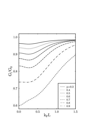
Variation of the conductance with the wall width (Fig.1) was calculated from Eq. (15), with the transmission coefficients determined numerically. Thus, the results shown in Fig. 1, are valid for arbitrary value of . The numerical modeling has been done by direct calculation of the spinor wave function using Eq. (2), starting at in a form of two transmitted spin up and down waves with arbitrary numerical coefficients. Then we restored the function in the region and, by numerical projecting the obtained spin components on the right- and left-moving waves (in accordance with Eq. (3)), we found the amplitudes of incident and reflected waves.
In the limit , the results shown in Fig.1 should coincide with those obtained from the formula (16). Comparison of the results obtained from direct numerical calculations and those obtained from Eq.(16) is shown in Fig. 2. Indeed the results coincide for , whereas at larger values of the deviations are large and grow with increasing .
The conductance in the presence of a domain wall is substantially smaller than in the absence of the wall. Accordingly, the associated magnetoresistance can be large. For example, for =0.9 in Fig.1 the magnetoresistance is equal to about 70% (which corresponds to ).

It should be noted that in a real magnetoresistance experiment on magnetic semiconductor nanowires, for which the inequality can be easily fulfilled, one can have more than one domain walls. Accordingly, the magnetoresistance effect can be significantly enhanced.
It is also worth to note that the resistance of an abrupt domain wall can be smaller than the resistance of a domain wall with finite (nonzero) thickness. This follows directly from the weak minimum in some of the curves in Fig. 1 (see also Fig. 2). The existence of this minimum is related to the sign of the second derivative of the function in Eq. (16), calculated at (the first derivative vanishes there). In our simple model, the corresponding sign is negative for (or, equivalently, ), and positive for (i.e., ). When increases from , the conductance decreases in the former case and increases in the latter one. On the other hand, we know that for thick domain walls the conductance increases with increasing wall thickness. Thus, the minimum should occur for the curves corresponding to . In the case of strong polarization, , the main contribution to the conductance is associated with the spin-flip transmission through the domain wall, and the conductance increases monotonously with the width of the domain wall, in accordance with Eq. (8).
IV Spin current
When the electric current is spin polarized and when there is some asymmetry between the two spin channels, the flow of charge is accompanied by a flow of spin (angular momentum). The -component of the spin current can be calculated from the following definition of the corresponding spin-current operator
| (24) |
which leads to the following average value
| (25) |
After carrying out the calculations similar to those described in the preceding section, one arrives in the linear response regime (limit of small bias voltage ) at the following formulas for the spin current :
| (26) |
| (27) |
Using Eqs. (6) we find
| (28) |
and . The magnetic torque due to spin transfer to the magnetic system within the domain wall is determined by the non-conserved spin current
| (29) |
It should be noted that spin-flip scattering due to DW does not allow to separate spin channels like it was in the case for homogeneous ferromagnets. If we define now the spin conductance as , then one can write for
| (30) |
Thus, is negative for and positive for .
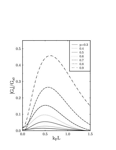
In a nonmagnetic case we have and therefore . In the case considered here, when there is no DW. Let us introduce the spin conductance for one (spin-up) channel only, . The relative spin conductance in the presence of DW, , calculated using Eq. (19) and with numerically found transmission coefficients, is shown in Fig. 3 as a function of the DW width and for the indicated values of the parameter . It corresponds to the spin current outside the region of the domain wall. The spin current inside the wall is not conserved because of the spin-flip transitions.
In accordance with Eqs. (19), (20) and (6), the nonzero spin current in a one-channel wire with domain wall is due to a difference in spin-flip transmissions for spin-up and spin-down channels: the corresponding transmission coefficient turns out to be larger for faster (majority) electrons.
V Spin polarization due to domain wall
Spin dependent reflections from the wall lead to additional spin polarization of the system near the wall. The distribution of spin density created by the wall can be calculated using the basis of scattering states. The -component of the spin density in the equilibrium situation () is
| (31) |
The above formula contains a constant part corresponding to the spin density in the absence of DW, as well as the -dependent part created by the wall,
| (32) |
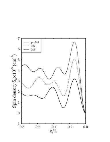
The dependence of the spin density on the distance from the wall is shown in Fig. 4. The spin dependent reflections from the wall create spatial oscillations of the electron spin density. These oscillations are similar to the Friedel oscillations of charge in a nonmagnetic metal. However, one should point out here that in addition to the above calculated spin polarization, there is also a nonequilibrium spin polarization due to flowing current.ebels00
VI Summary and concluding remarks
We have presented in this paper a theoretical description of the resistance of a magnetic microjunction with a constrained domain wall at the contact. In the limit of , the electron transport across the wall was treated effectively as electron tunneling through a spin-dependent potential barrier. For such narrow and constrained domain walls the electron spin does not follow adiabatically the magnetization direction, but its orientation is rather fixed. However, the domain wall produces some mixing of the spin channels.
The calculations carried out in the paper were restricted to a limiting case of a single quantum transport channel. Accordingly, the system was described by a one-dimensional model. However, such a simple model turned out to describe qualitatively rather well the basic physics related to electronic transport through constrained domain walls, although the magnetoresistance obtained is still smaller than in some experiments. In realistic situations one should use a more general model. When the domain wall does not cause transition between different channels, then the description presented here can be applied directly to the multichannel case by simply adding contributions from different channels.
A domain wall leads to spin dependent scattering of conduction electrons. Therefore, it also leads to a net spin polarization at the wall, which oscillates with the distance from the wall, similarly to Friedel oscillations of charge density near a nonmagnetic defect in a nonmagnetic metal. We have calculated the equilibrium component of this spin polarization.
It should be also pointed out that our description neglects electron-electron interaction. Such an interaction is known to be important in one-dimensional systems, particularly in the limit of zero bias. The interaction may lead to some modifications of the results in a very small vicinity of , but we believe that the main features of the magnetoresistance will not be drastically changed.
Acknowledgements.
We thank P. Bruno for very useful discussions. This work is partly supported by Polish State Committee for Scientific Research through the Grant No. PBZ/KBN/044/P03/2001 and INTAS Grant No. 2000-0476.References
- (1) A. D. Kent, J. Yu, U. Rüdiger, and S. S. P. Parkin, J. Phys. Cond. Matter 13, R461 (2001).
- (2) K. Hong and N. Giordano, J. Phys. Condens. Matter 13, L401 (1998).
- (3) U. Rüdiger, J. Yu, S. Zhang, A. D. Kent, and S. S. P. Parkin, Phys. Rev. Lett. 80, 5639 (1998).
- (4) A. D. Kent, U. Rüdiger, J. Yu, L. Thomas, and S. S. P. Parkin, J. Appl. Phys. 85, 5243 (1999).
- (5) J. F. Gregg, W. Allen, K. Ounadjela, M. Viret, M. Hehn, S. M. Thompson, and J. M. D. Coey, Phys. Rev. Lett. 77, 1580 (1996).
- (6) N. Garcia, M. Muoz, and Y.-W. Zhao, Phys. Rev. Lett. 82, 2923 (1999).
- (7) U. Ebels, A. Radulescu, Y. Henry, L. Piraux, and K. Ounadjela, Phys. Rev. Lett. 84, 983 (2000).
- (8) G. Tatara and H. Fukuyama, Phys. Rev. Lett. 78, 3773 (1997).
- (9) P. M. Levy and S. Zhang, Phys. Rev. Lett. 79, 5110 (1997).
- (10) R. P. van Gorkom, A. Brataas, and G. E. W. Bauer, Phys. Rev. Lett. 83, 4401 (1999).
- (11) P. A. E. Jonkers, S. J. Pickering, H. De Raedt, and G. Tatara, Phys. Rev. B 60, 15970 (1999).
- (12) G. Tatara, Int. J. Mod. Phys. B 15, 321 (2001).
- (13) R. Danneau, P. Warin, J.P. Attané, I. Petej, C. Beigné, C. Fermon, O. Klein, A. Marty, F. Ott, Y. Samson, and M. Viret, Phys. Rev. Lett. 88, 157201 (2002).
- (14) H. D. Chopra and S. Z. Hua, Phys. Rev. B 66, 020403(R) (2002).
- (15) P. Bruno, Phys. Rev. Lett. 83, 2425 (1999).
- (16) G. G. Cabrera and L. M. Falicov, Phys. Status Solidi B 61, 539 (1974); 62, 217 (1974).
- (17) A. Brataas, G. Tatara, and G. E. W. Bauer, Phys. Rev. B 60, 3406 (1999).
- (18) E. Simanek, Phys. Rev. B 63, 224412 (2001).
- (19) V. K. Dugaev, J. Barnaś, A. Łusakowski, and Ł. A. Turski, Phys. Rev. B 65, 224419 (2002).
- (20) H. Imamura, N. Kobayashi, S. Takahashi, and S. Maekawa, Phys. Rev. Lett. 84, 1003 (2000).
- (21) L. R. Tagirov, B. P. Vodopyanov, and K. B. Efetov, Phys. Rev. B 65, 214419 (2002); Phys. Rev. B 63, 104428 (2001); L. R. Tagirov, B. P. Vodopyanov, and B. M. Garipov, J. Magn. Magn. Mater. 258-259, 61 (2003).
- (22) J. B. A. N. van Hoof, K. M. Schep, A. Brataas, G. E. W. Bauer, and P. J. Kelly, Phys. Rev. B 59, 138 (1999).
- (23) J. Kudrnovsky, V. Drchal, C. Blaas, P. Weinberger, I. Turek, and P. Bruno, Phys. Rev. B 62, 15084 (2000).
- (24) J. Kudrnovsky, V. Drchal, I. Turek, P. Streda, and P. Bruno, Surf. Sci. 482-485, 1107 (2001).
- (25) B. Yu. Yavorsky, I. Mertig, A. Ya. Perlov, A. N. Yaresko, and V. N. Antonov, Phys. Rev. B 66, 174422 (2002).