Transfer of magnetization by spin injection between both interfaces of a Ni nanowire
Abstract
Magnetization switching provoked by spin-injection is studied in Ni nanowires of various size and morphology. The response of the magnetization to the spin-injection is studied as a function of the amplitude of the current, the temperature, and the symmetry of the interfaces. The amplitude of the response of the magnetization to spin-injection is a decreasing function of the temperature, does not depend on the current sign, and occurs only in the case of asymmetric interfaces. It is shown that the spin-injection does not act on small magnetic inhomogeneities inside the layer. Some consequences in terms of longitudinal spin-transfer are discussed.
pacs:
75.40.Gb, 75.60.Jk,75.60.LrThe possibility of driving magnetization states without the need of a magnetic field was predicted some years ago by Berger Berger and independently by J. Slonczewski Sloncz . This effect is observed today, especially with giant magnetoresistance (GMR) in nanopillar structures Albert , and is interpreted in terms of spin-transfer. However, current induced magnetization switching (CIMS) effects are also measured in homogeneous and nanowires EPL ; SPIE , and in domain wall systems Klaui where no GMR can be measured. Is the mechanism responsible for CIMS different in these cases? Previous studies tend to show that both effects may be identical SPIE .
The aim of this letter is to investigate further CIMS in a single magnetic layer by measuring the amplitude of the effect as a function of the temperature, of the amplitude and sign of the injected current, of the symmetry of both interfaces, and by studying the effect of the current on small magnetic inhomogeneities inside the wire. In order to modify the symmetry of the interface with respect to the spin-injection, two kinds of samples have been measured. Samples of kind are (200 nm)/(6 m / ) and samples of kind B are (200 nm)/(X m)/(6-X m / ) obtained by electrodeposition in nanoprous polycarbonate membrane templates Meier . The membrane thickness is six micrometers, and the diameter of the pores is about 60 nanometers. The electrodeposited is composed of small nanocrystallites, so that the system is quasi amorphous with respect to the magnetic properties. The anisotropy is then reduced to the shape anisotropy, defined by the aspect ration of the nanowires PRL . This is the reason why these experiments are performed with , and not with nanowires where CIMS are also observed.
In samples of kind , is electrodeposited up to the top of the membrane, where a second thin layer (45 nm) was deposited previously. The top layer do not close the pores and its function is to measure the potential between the top and the bottom of the membrane during the electrodeposition, in order to obtained a single wire contact. The contact is formed by a mushroom of a few hundreds of nm to one micrometer Travis . On the other hand, in the sample of kind electrodeposition is stopped after a calibrated time inside the pores, and the rest of the deposition, including the contact, is performed with . Note that and the are identical with respect to the spin injection (zero spin polarization of the current). As a consequence, in samples of kind , the spin injection on the top interface is performed with a geometry close to the current in plane of the ferromagnetic layer (CIP), and with the geometry current perpendicular to the plane (CPP) on the bottom interface. In contrast, the samples of kind have current injection with CPP geometry for both interfaces, and are symmetric to that respect.
The hysteresis loop is measured with the anisotropic magnetoresistance with a field applied at about from the wire axis (Fig. 1). This angle is chosen because the signal due to the irreversible magnetization reversal reaches its maximum amplitude PRL . The resistance of the sample is 148 at 150K, in agreement with the resistivity of and the wire diameter of 60 nanometers. Both half-hysteresis loops (for decreasing fields and for increasing fields) are symmetric, and are composed by a reversible part (equilibrium states of the magnetization), and a single irreversible jump, which occurs at the switching field . The sample is chosen in such a way that all equilibrium states are uniform magnetization states within about two percent of the total magnetization. This can be checked by fitting the envelope of the curve with the uniform reversal model, and applying the curve obtained for different angles of the external field. The irreversible jump occurs at a critical angle , related to a critical field (spinodal limit). Detailed studies of the magnetic states are reported elsewhere PRL . The magnetic configurations are uniform for all temperatures, but the anisotropy of the nanowire increases dramatically when the temperature is decreased from room temperature down to Helium temperature, as observed in previous studies Meier . Beyond the change in magnetic anisotropy, the AMR decreases from 1.5 % at 200 K down to 1% at 4.5K in contrast to the measured bulk AMR Potter : this is due to the finite size effect as predicted and quantified in reference Rijks .
The effect of the current is studied by injecting a pulsed current of one microsecond duration (about 100 ns rising time) at a given magnetization state. The magnetization state is described equivalently by its angle EPL or by the distance to the switching field (Fig. 1). This distance is a measure of the barrier hight to be overcome by the magnetization switch SPIE , due to current injection, from one equilibrium state to the other (two states system). Consequently, the maximum distance where the magnetization reversal can still be observed gives the amplitude of the effect of the current on the magnetization.
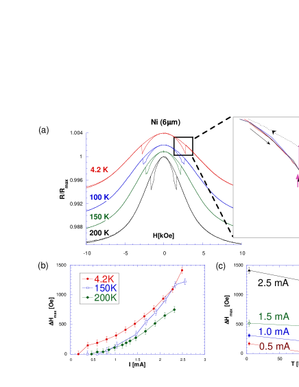
The parameter is plotted as a function of the current amplitude (Fig. 1(b)) for different temperatures. The curves are reproducible, and do not depend on the sign of the current! The amplitude of the effect is of the order of 1 kOe (0.1 Tesla) for 2 mA injection, while the maximum induced field (Oersted field produced radialy by the current) is below 100 Oe (0.01 Tesla) and has a radial symmetry. The effect of the induced field as been ruled-out in previous works EPL ; SPIE . The slope is about 500 Oe/ mA (or about 25 mT/(10-7 A/cm2)) which is typical in such samples EPL , and is of the same order of magnitude as what has been measured in pillar structures ( in the same units : 20, 20, 16 reported in Albert ). The temperature dependence (Fig. 1(c)) varies from a factor 1.5 between 200 K and 4.2K. This temperature dependence has not been reported so far in nanowires, and is opposite to that measured in pillar samples Albert . This observation seems to indicate that CIMS is directly related to the spin diffusion length.
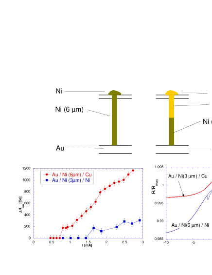
The comparison between samples of kind and samples of kind (resistance R=112 at 150 K) shows that there is a qualitative difference (Fig 2(a)) of the response of the magnetization to the current excitation. The hysteresis loops show the variation in terms of AMR (the reduction in sample is due to the fact that the active part of the device is reduced by a factor 2, with approximately constant total resistance), and in terms of anisotropy due to the reduction of the aspect ratio of the nanowire. A statistical ensemble of samples of both kinds have been measured, with varying the parameters of the deposition, like the pH and the concentration of the solution. A series of samples of kind have been measured with varying the size of the layer. The result is always similar to that presented in Fig. 2(a). The response of the magnetization to the current injection is negligible in the case of the samples of kind , and this result is independent of the anisotropy, and more generally independent of the energy barrier of the magnetic layer (proportional to the volume of the layer). In all cases, the curves are reproducible, and do not depend on the current direction.
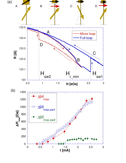
In order to investigate further the role of the contact on the top of the membrane, we focalized our attention to the presence of a small inhomogeneity in the wire (Fig. 3). The envelop of the hysteresis loop is identical to the usual ones, but a zoom of the irreversible part of the hysteresis shows the nucleation of an inhomogeneity, which should be a pinned vortex or any constrained domain wall in the top of the membrane (the position of the inhomegeneity has not been directly measured, but wires with Cu contacts do not exhibit such structures). The deviation to the uniform rotation of the magnetization shows that the inhomogeneity inside the wire is of the order of 2 % of the total magnetization, i. e. about 100 nm (the magnetization of the contact is not measured since the current density is negligible). A minor loop can be obtained if the external field is swept back after the creation of the inhomogeneity (field ), but before its annihilation at higher field. The minor hysteresis loop describes then the different magnetization states with the inhomogeneity (sketched in Fig. 3(a)). (A) the magnetization of the contact makes an angle close to that of the nanowire, there is no significant inhomogeneity. (B) The magnetization of the contact is in the direction of the applied field. Exchange coupling induced an inhomogenoeity inside the wire (point B). The annihilation of the inhomogeneity occurs at higher fields because the angle of the magnetization of the nanowire is close to the external field. If the external field is swept back before the annihilation field, the inhomogeneity is maintained (and compressed) from point B to point D, at which the homogeneous state is restored.
The response of the whole magnetization to the current injection is not significantly affected by the inhomogeneity. If is the amplitude of the effect after following the minor loop (i.e. with the presence of the inhomogeneity) and is the direct loop (no inhomogeneity in the region AB), we have (Fig. 3(b)). Furthermore, the current injection does not act on the annihilation (D) of the inhomogeneity : the jump is not significantly affected by the current injection (and the variation Oe can be attributed to the field induced by the current).
In conclusion, we have to deal with the three following observations : (1) the sign of the current does not play any role (in contrast to CIMS in GMR pillar structures), (2) the presence of the asymmetry is necessary for CIMS, (3) the current acts on the whole structure composed by the wire and both interfaces, and not locally. All occurs as if CIMS effects were due to an imbalance of the spin-injection between both interfaces of the layer. In this picture, a spin transfer occurs at the first normal/ferromagnet interface, which should be compensated at the second ferromagnetic/normal interface. If an imbalance exists between both interfaces due to an asymmetry with respect to spin injection, a longitudinal spin transfer can be expected from the current to the magnetic layer. This hypothesis is corroborated by the fact that in the GMR pillars (in contrast to homogeneous nanowires) the change in the direction of the current leads to a change in the response of the magnetization as much as changing the magnetic configuration from parallel to antiparallel SPIE . Indeed, as described by Berger Beger, the asymmetry between the two interfaces (in terms of spin-polarization) is not only due to the spin injection Berger ; wegrowe but also to the spin accumulation where the sign depends on the sign of the current. It is then expected that, in contrast to the homogeneous wires, the imbalance due to the asymmetry is reversed by changing the sign of the current.
References
- (1) L. Berger, J. Appl. Phys., 55, 1954 (1984), L. Berger, Phys. Rev. B 54, 9353 (1996) and L. Berger J. Appl. Phys. 93, 7693 (2003).
- (2) J. C. Slonczewski, J. Magn. Magn. Mat. 159 L1 (1996).
- (3) F. J. Albert, J. A. Katine, R. A. Buhrman, D. C. Ralph, Appl. Phys. Lett. 77 3809 (2000), J. Grollier, V. Cros, A. Hamzic, J.M. George, H. Jaffes, A. Fert, G. Faini, J. Ben Youssef, H. Le Gall, Appl. Phys. Lett. 78, 3663 (2001), J. Z. Sun, D. J. Monsma, D. W. Abraham, M. J. Rooks and R. H. Koch, Appl. Phys. Lett. 81, 2202 (2002), J.-E. Wegrowe, A. Fabian, X. Hoffer, Ph. Guittienne, D. Kelly, E. Olive, J.-Ph. Ansermet Appl. Phys. Lett. 91, 6806 (2002), S. Urazhdin, H. Kurt, W. P. Pratt, and J. Bass, Appl. Phys. Lett. 83 114 (2003), S. Urazhdin et al. cond-mat/03031492.
- (4) J-E Wegrowe, D. Kelly, Y. Jaccard, Ph. Guittienne, J-Ph Ansermet, Europhys. Lett. 45, 626 (1999), J-E Wegrowe et al. Europhys. Lett. 56, 748 (2001) and D. Kelly et al. accepted for publication in PRB.
- (5) J.-E. Wegrowe cond-mat/0306103.
- (6) M. Klaüi et al. Appl. phys. Lett. 83 (2003), 105, J. Grollier et al. Appl. Phys. Lett. 83 (2003).
- (7) J. Meier, B. Doudin, and J.-Ph. Ansermet, J. Appl. Phys. 79, 6010 (1996).
- (8) J.-E. Wegrowe, D. Kelly, A. Franck, S.E. Gilbert, J.-Ph. Ansermet, Phys. Rev. Lett. 82 3681(1999) and Y. Jaccard et al. Phys. Rev B 62, 1141 (2000).
- (9) Ch. Schönenberger et al., J. Phys. Chem. B, 101 (1997), 5497.
- (10) T. R. McGuire and R. I. Potter, IEEE Trans. Mag.-11 (1975), 1018.
- (11) Th. G. S. M. Rijks, R. Coehoorn, M. J. M. de Jong, W. J. M. de Jonge, Phys. Rev. B, 51 (1995), 283.
- (12) J.-E. Wegrowe, Phys. Rev. B 62, 1067 (2000).