Theoretical study on novel electronic properties
in nanographite materials
Kikuo Harigaya1,2,111Corresponding author; FAX: +81-29-861-5375; E-mail: k.harigaya@aist.go.jp, Atsushi Yamashiro1, Yukihiro Shimoi1,2, Katsunori Wakabayashi3, Yousuke Kobayashi4, Naoki Kawatsu4, Kazuyuki Takai4, Hirohiko Sato5,
Jérôme Ravier4, Toshiaki Enoki4, and Morinobu Endo6
1Nanotechnology Research Institute, AIST,
Tsukuba 305-8568, Japan
2Synthetic Nano-Function Materials Project,
AIST, Tsukuba 305-8568, Japan
3Dept. of Quantum Matter Science,
Hiroshima University, Higashi-Hiroshima 739-8530, Japan
4Department of Chemistry,
Tokyo Institute of Technology, Meguro-ku 152-8551, Japan
5Department of Physics, Chuo University,
Bunkyo-ku 112-8551, Japan
6Faculty of Engineering, Shinshu University,
Nagano-shi 380-8553, Japan
Abstract
Antiferromagnetism in stacked nanographite is investigated with
using the Hubbard-type model. We find that the open shell
electronic structure can be an origin of the decreasing magnetic
moment with the decrease of the inter-layer distance, as
experiments on adsorption of molecules suggest. Next, possible
charge-separated states are considered using the extended
Hubbard model with nearest-neighbor repulsive interactions. The
charge-polarized state could appear, when a static electric field
is present in the graphene plane for example. Finally,
superperiodic patterns with a long distance in a nanographene
sheet observed by STM are discussed in terms of the interference
of electronic wave functions with a static linear potential
theoretically. In the analysis by the model, the oscillation
period decreases spatially in agreement with experiments.
Keywords: A. inorganic compounds, A. magnetic materials, C. scanning tunnelling microscopy (STM), D. magnetic properties, D. electronic structure
1. Introduction
Nanographite systems, where graphene sheets of the orders of the nanometer size are stacked, show novel magnetic properties, such as, spin-glass like behaviors [1], and the change of ESR line widths while gas adsorptions [2]. It has been found [3, 4] that magnetic moments decrease with the decrease of the interlayer distance while water molecules are attached physically. Such the phenomena indicate the tunable magnetism in nanometer size systems. Recently, unique magnetisms in carbon-based materials have been observed [5, 6], and thus theoretical investigations are urged in order to resolve the mechanisms.
This paper reviews recent theoretical works on electronic properties in nanographite materials, and is organized as follows. (1) Antiferromagnetism in the stacked nanographite is investigated with using the Hubbard-type model taking into account of the hopping interactions of -electrons and the strong onsite repulsions at carbon atoms [7, 8]. We point out the importance of the open shell electronic structure as an origin of the decreasing magnetic moment with the decrease of the inter-layer distance [3, 4]. (2) Possible charge-separated states in nanographite ribbons are discussed in terms of the extended Hubbard model with nearest-neighbor interactions [9]. Such the charge-polarized state could be observed, when a static electric field is applied in the direction parallel with the graphene plane for example. (3) Superperiodic patterns with a long distance in a nanographene sheet observed by STM are discussed in terms of the interference of electronic wave functions. The period and the amplitude of the oscillations decrease spatially in one direction. We explain the superperiodic patterns with a static linear potential in the model [10].
2. Tuning magnetism in stacked nanographite
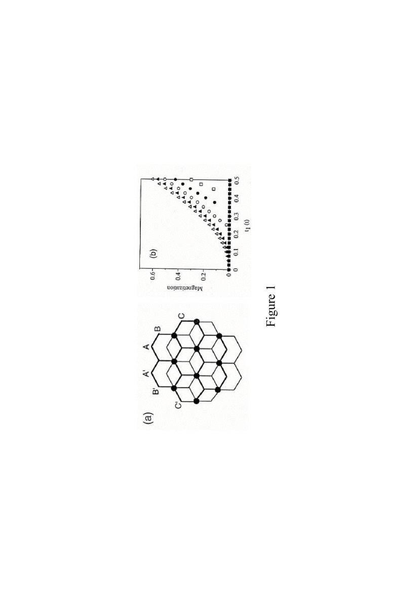
First, we report magnetic properties for the A-B stacked hexagonal nanographite shown in Fig. 1 (a) [7]. The first and second layers are displayed by the thick and thin lines, respectively. In each layer, the nearest neighbor hopping is considered. Each layer has closed shell electron systems when the layers do not interact mutually, because the number of electrons is even and equal to the number of sites. The interlayer hopping is assigned at the sites with closed circles. The model is solved with the unrestricted Hartree-Fock approximation, and antiferromagnetic solutions are obtained. Figure 1 (b) shows the absolute value of the total magnetic moment per layer as functions of and . As increasing , the magnitude of the magnetization increases. The magnetic moment is zero at the smaller region for (open squares), (closed circles), and (open circles). The magnetic moment is zero only at for (closed triangles) and (open triangles). We can understand the parabolic curves as a change due to the Heisenberg coupling proportional to .
Next, we consider systems with open shell electronic structures when a nanographene layer is isolated [8]. One case is the effects of additional charges coming from functional side groups with introducing a site potential at edge sites. We take , and one additional electron per layer is taken account. Figure 2 displays the absolute values of total magnetic moment per layer. In Fig. 2 (a), the site potentials locate at the site A in the first layer [Fig. 1 (a)], and at its symmetrically equivalent site in the second layer. In Fig. 2 (b), the site potential exists at the site B. The total magnetization is a decreasing function of in both figures. The decrease is faster in Fig. 2 (b) than in Fig. 2 (a). The site B is neighboring to the site with the interaction , and thus the localized character of the magnetic moment can be affected easily in this case. The decease of observed magnetization by the magnitude % with the water molecule attachment [3, 4] may correspond to the case of Fig. 2 (b). The other origin, i.e., the geometrical effects can give rise to the decrease of the magnetic moment with increasing interlayer hopping interactions, too. Therefore, we conclude that the open shell nature of electronic states in a single graphene layer plays an important role in controlling the magnetism in nanographite materials.
3. Charge- and spin-separated states in nanographite ribbons
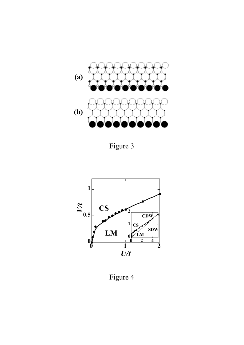
In section 2, we have discussed the magnetic properties with using the onsite interactions only. In this section, we will report a possible charge-separated state in nanographite ribbons with zigzag edges by introducing the nearest-neighbor Coulomb repulsion term as well as [9]. The model is solved with a mean field method with the finite space geometry shown in Fig. 3. Charge- and spin-polarized solutions are obtained depending on the interaction strengths. For example, Fig. 3 (a) shows the charge density distribution of the ferroelectric charge separated (CS) state with and . This state appears and becomes stable when the effects of overcom those of . On the other hand, Fig. 3 (b) shows the spin density profile of the localized magnetic (LM) state for and . This state is stable when is weak. The CS (LM) state has no spin (charge) density at every site. In the CS state, the upper (lower) zigzag edge is charged positively (negatively). This distribution pattern is quite similar to that in the LM state. Such the static charge polarization (magnetization) is explained by the interplay of the Fermi instability of the flat bands due to () and the localized edge states. The signs of the charge (spin) densities at neighboring sites are opposite, reflecting the bipartite nature.
Figure 4 shows the phase diagram in the parameters and , representing the stability between the CS and LM states. We use the geometry with carbon atoms. Above the phase boundary, the CS state has the lower energy, and the LM state becomes stable below the boundary. The phase boundary indicates the first order phase transition. At , the phase boundary rises up with the infinite gradient. This is a signature of the localized edge states, differently from the graphite sheet. The inset shows the phase diagram in reduced scales. In the strong correlation limit, the phase boundary approaches to an analytical phase boundary line between the CDW and SDW states, which is obtained by equalizing their Coulomb energies. Here, is the number of zigzag lines of the ribbon. The CDW and SDW solutions are crossovered from those of CS and LM for the weak interactions. Such the charge-separated states could be observed when static electric field is applied in the nanographene plane for example, and the presence of the state will give effects on dielectric properties.
4. Electronic wave interference patterns
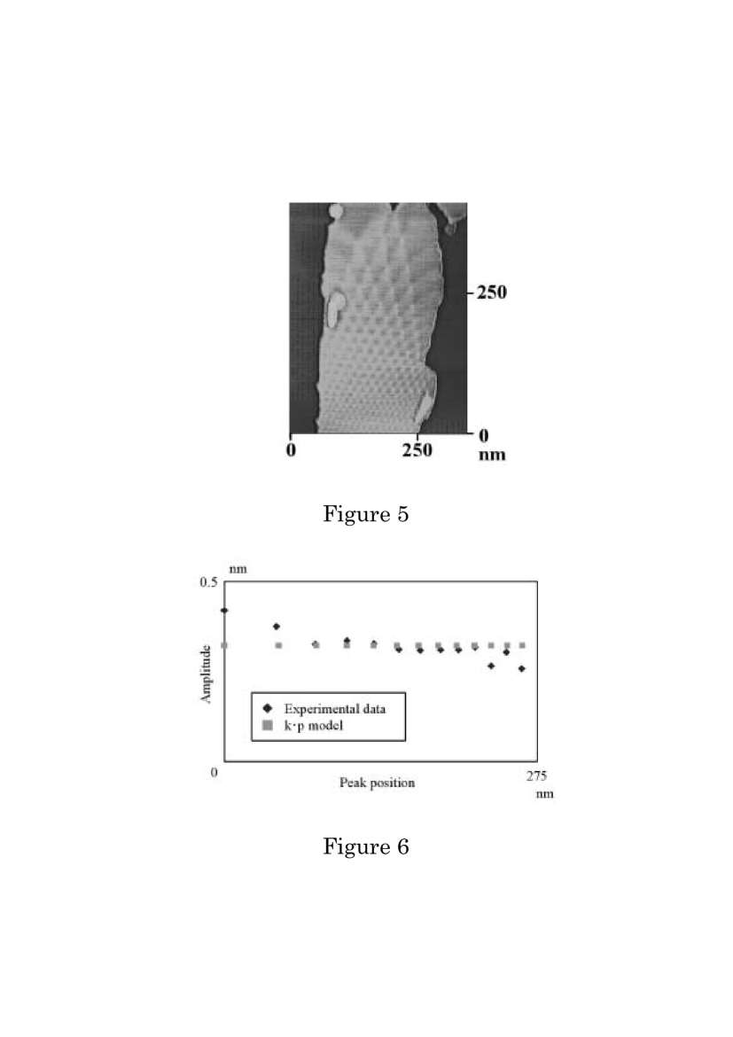
In Fig. 5, an STM image of the graphene sheet with a necktie shape is shown [10]. The observation has been done with the following condition: bias voltage mV and current nA. The distance between the graphene necktie and the substrate is over 0.8 nm, suggesting that it consists of a stacking of two graphene layers, which interact weekly with the HOPG substrate. Interestingly, the period and the amplitude of the oscillations decrease from the top to the bottom along the graphene necktie. The oscillation period is one order of magnitude larger than that of the Moiré pattern due to stacking, which has been reported elsewhere, and therefore this possibility may be weak. We can assume effects of long-distance periodic-structural deformations in the graphene surface or interference effects of electronic wave functions. We have also observed that the oscillation period becomes longer by placing a nanographene flake on the graphene necktie. The oscillations period seems to be double in the upper region of the necktie after addition of one flake. The oscillation below the flake seems to be only slightly modified by the flake. Such effect on the oscillations cannot be explained by some structural modulations. Therefore, the oscillation patterns could be the effect of interference of the electronic wave functions in the graphene surface.
In order to analyze the interference patterns, we give comparison with the calculation of the model for the graphene plane. Here, we use the continuum model [10]. The electron density is calculated with including a static potential which has a functional form of the linear decrease from top to the bottom along the surface of the graphene necktie. The peak positions of the electron density in the long direction of the graphene necktie of Fig. 5 are plotted in Fig. 6, and comparison with the theoretical results is given. The decrease of the oscillation period fairly agrees with the experiments. However, the slight decrease of the experimental corrugation cannot be reproduced by the theoretical result because of neglecting an effect of a tip-apex shape of STM on the observed corrugatrion amplitude. The fitting gives the parameter of the potential gradient eV/nm. The total potential variation over the distance 200 nm becomes 1.3 eV. Such magnitude of the potential change would survive under thermal lattice fluctuations and can really exist in experiments. The present result by no means implies that the wave functions observed with superperiodic amplitudes are of the electrons which have energy levels of the graphene plane.
5. Summary
First, antiferromagnetism in the stacked nanographite has been investigated with the Hubbard-type model. The A-B stacking is favorable for the hexagonal nanographite with zigzag edges, in order that magnetism appears. We have also found that the open shell electronic structures can be origins of the decreasing magnetic moment with adsorption of molecules.
Next, possible charge-separated states have been considered using the extended Hubbard model with nearest-neighbor interactions. The charge-polarized state could appear, when a static electric field is applied in the graphene plane for example.
Finally, we have characterized theoretically the superperiodic patterns in a nanographene sheet observed by STM. We have adopted the model for the description of the electronic structures of the graphite. The calculated electron density has the property that the oscillation period decreases spatially while the amplitude remains constant. The magnitude of the static potential seems reasonable. It turned out that the long distance oscillations come from electrons with the band structures of the two dimensional graphene sheet.
Bibliography
- [1] Y. Shibayama et al, Phys. Rev. Lett. 84, 1744 (2000).
- [2] N. Kobayashi et al, J. Chem. Phys. 109, 1983 (1998).
- [3] T. Enoki et al, Polyhedron 20, 1311 (2001).
- [4] H. Sato et al, Solid State Commun. 125, 641 (2003).
- [5] T. L. Makarova et al, Nature 413, 716 (2001).
- [6] J. M. D. Coey et al, Nature 420, 156 (2002).
- [7] K. Harigaya, J. Phys.: Condens. Matter 13, 1295 (2001).
- [8] K. Harigaya and T. Enoki, Chem. Phys. Lett. 351, 128 (2002).
- [9] A. Yamashiro, Y. Shimoi, K. Harigaya, and K. Wakabayashi, (preprint).
- [10] K. Harigaya et al, J. Phys.: Condens. Matter 14, L605 (2002).
Figure Captions
Fig. 1. (a) A-B stacked hexagonal nanographite with zigzag edges. (b) The absolute magnitude of the total magnetic moment per layer as a function of . The onsite interaction is varied within (closed squares) (open triangles). The interval of between the series of the plots is .
Fig. 2. The absolute magnitude of the total magnetic moment per layer as a function of for the system with a site potential , (a) at the site A and (b) at the site B. The site positions are displayed in Fig. 1 (a). In (a), the onsite interaction is varied within (closed squares) (closed triangles) with the interval . In (b), it is varied within (closed squares) (closed triangles) with the interval .
Fig. 3. (a) Charge density distribution of the charge-separated (CS) state, and (b) the spin density distribution of the localized magnetic (LM) state on a zigzag ribbon with carbon atoms, where means positive charge (spin) densities, and indicates negative charge (spin) densities. The radius of each circle denotes the magnitude of the density.
Fig. 4. The phase diagram in the parameter space of and for a zigzag ribbon with carbon atoms. The solid curve is the boundary between the CS and LM states, interpolating the numerical data (). The inset shows the phase diagram in reduced scales. The dashed line denotes the phase boundary in the strong correlation limit.
Fig. 5. STM image of the superperiodic pattern observed on a necktie shaped graphene plate on HOPG substrate.
Fig. 6. Comparison for the electron wave patterns by STM and the model. Experimental peak positions along the perpendicular direction of Fig. 5 are plotted by diamonds. The results of the fitting by the long distance envelope functional form derived from the model are shown by squares.