Enhanced shot noise in resonant tunnelling via interacting localised states
Abstract
In a variety of mesoscopic systems shot noise is seen to be suppressed in comparison with its Poisson value. In this work we observe a considerable enhancement of shot noise in the case of resonant tunnelling via localised states. We present a model of correlated transport through two localised states which provides both a qualitative and quantitative description of this effect.
pacs:
73.20.Hb, 73.40.Gk, 72.70.+mUnderstanding the role of electron coherence and Coulomb interaction in electron transport is one of the main directions of contemporary research in mesoscopic physics. Recently, shot noise measurements have proved to be a useful tool for these studies, since they provide information which is not available from standard conductance measurements Blanter!Buttiker!Review . Shot noise, i.e. fluctuations of the current in time due to the discrete nature of electrons, is a measure of temporal correlations between individual electron transfers through a mesoscopic system. Uncorrelated transfers result in the Poisson shot noise with the noise power ( is the electron charge, and is the average current). The effects on noise of the Pauli exclusion principle Les and the Coulomb repulsion Korotkov turn out to be similar in most mesoscopic systems. Both were predicted to impose a time delay between two consecutive electron transfers, which results in negative correlations between them and, therefore, suppression of shot noise. This idea has been intensively explored in studies of the shot noise properties in ballistic and diffusive systems QPC ; One!Third .
Electron transport via localised states in a potential barrier between two contacts has been a subject of intensive investigations. If the size of a mesoscopic barrier is small, resonant tunnelling (RT) through a single localised state (impurity) becomes responsible for conduction across the barrier Fowler . When the resonant level () coincides with either of the Fermi levels in the contacts, , a peak in the conductance appears. The amplitude of the peak is determined by the ratio of the leak rates from the resonant impurity to the contacts, where are the distances between the impurity and the left or right contacts, and is the localisation radius of the state, Fig.1a. The current is given by the relation . It has been predicted in Ting ; Nazarov that for RT via a localised state shot noise is suppressed by the Fano factor . The Fano factor then ranges from 0.5 (for equal rates) to 1 (for significantly different rates) dependent on the position of the resonant impurity inside the barrier. Suppression of shot noise in accordance with this relation has been first observed in a resonant tunnelling structure Old . Similar suppression of shot noise in the Coulomb blockade regime has been seen in a quantum dot Schonenberger . In electron hopping (sequential tunnelling) through equivalent barriers the Fano factor is also expected to be suppressed, , if one assumes that the Poisson noise is generated across a single barrier Kuznetsov!Hopp .
In this work we present a study of time-dependent fluctuations of the RT current through a short (0.2 m) tunnel barrier. Surprisingly, we observe a significant enhancement of shot noise with respect to the Poisson value. We explain this effect by correlated resonant tunnelling involving two interacting localised states.
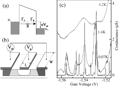
The experiment has been carried out on a n-GaAs MESFET consisting of a GaAs layer of m (donor concentration cm-3) grown on an undoped GaAs substrate. On the top of the structure an Au gate is deposited with dimensions m in the direction of the current and m across it, Fig.1b. By applying a negative gate voltage, , a lateral potential barrier is formed between the ohmic contacts (source and drain). Its height is varied by changing . When a source-drain voltage is applied, fluctuations of the current between the ohmic contacts are measured by two low-noise amplifiers. The cross-correlation spectrum in the frequency range kHz is detected by a spectrum analyzer Roshko . This technique removes noise generated by the amplifiers and leads.
Fig.1c shows an example of conductance peaks as a function of in the studied sample at and different temperatures down to K. One can see that with lowering temperature the background conduction (due to electron hopping) decreases and the amplitude of the conductance peaks increases. This increase is a typical feature of resonant tunnelling through an impurity Fowler .

The box in Fig.2a indicates the range of where shot noise has been studied at 1.85 K K. In Fig.2b (inset) an example of the excess noise spectrum is shown at a gate voltage near the RT peak in Fig.2a. (In this spectrum thermal noise has been subtracted and the effect of the stray capacitance has been taken into account according to Roshko .) Shot noise is determined from the flat region of the spectrum above 40 kHz. In this region one can neglect the contribution of noise () which is shown in Fig.2b (inset) by a solid line.
Fig.2b shows the dependence of the shot noise power on at two temperatures. At small biases ( mV) a pronounced peak in noise is observed with an unexpectedly large Fano factor . This is seen by plotting the dependences with different using the phenomenological expression for excess noise in the case of RT through a single impurity (cf. Eq.(62) in Blanter!Buttiker!Review and Eq.(11) in Nazarov ):
| (1) |
(The expression describes the evolution of excess noise into shot noise at ; is the ohmic conductance of the sample) At large biases ( mV), however, shot noise decreases to a conventional sub-Poisson value, .
We have established that the increase of shot noise exists only in a specific range of . It is worth noting that there is no negative differential conductance in the region of - where the peak in the noise appears, and, therefore, we cannot link this enhancement to some sort of instability Blanter!Buttiker!NDC . Instead, we will show that in this region of - the resonant current is carried by two interacting impurities and this leads to the increase of shot noise.
We will first show that interaction between two states can considerably increase shot noise. Let us start with a simple illustrative model and consider two spatially close impurity levels, and , separated in the energy scale by . If impurity is charged, the energy level of is shifted upwards by the Coulomb energy , where is the separation between the impurities and is the dielectric constant, Fig.3 (diagram 1). Thus, dependent on the occupancy of , impurity can be in two states: or . Further we assume that is small enough so that state is above the Fermi level in the left contact, Fig.3 (diagram 2). Then electrons are transferred via with the rates if is empty, and cannot be transferred if is charged. It is assumed that impurity changes its states independently of the state of impurity : from empty to charged state with the rate and from charged to empty state with the rate . If changes its occupancy at a slow rate, i.e. , its contribution to the current is negligible and we will call a modulator since it modulates the current through impurity . This current jumps randomly between two values: zero, when is occupied, and when is empty, Fig.3 (inset). If the bias is increased, the upper state is shifted down into the conducting energy strip and the modulation of the current via impurity vanishes, Fig.3 (diagram 3).
In the modulation regime, the average current through impurity and the corresponding zero-frequency Fano factor can be written, respectively, as
| (2) |
and
| (3) |
The first term in Eq.(3) describes the suppression of the Fano factor below unity Nazarov , whereas the second term gives a positive contribution. To illustrate the origin of the second term, one can think of the modulated current as random telegraph noise (RTN), i.e. spontaneous jumps between zero and . The second term can then be obtained from the spectrum of RTN Kirton!Uren with characteristic times of the upper and lower states - and , respectively. If , a substantial enhancement of shot noise, , is expected from Eq.(3). Another way to illustrate the origin of this effect is to assume that is close to the left contact. As a result, impurity spends more time in its charged state, i.e. and the current through is transferred in bunches, with the average duration of a bunch . The noise due to the ‘chopping’ of the current can then be estimated as , where is the average charge transferred in one bunch. This charge is equal to , and this again gives the second term in Eq.(3).
This model of a slow modulator which changes its state independently of impurity may look too simplistic. However, its generalisation (for any relation between and ) is straightforward and provides a consistent quantitative description of the observed effect. Our theoretical model is based on the master equation formalism Nazarov ; Glazman!Matveev . It is applicable when - the condition satisfied in our experiment. Then the system of two interacting impurities and can be in four possible states. The transition rates between these states are determined by tunnelling between the contacts and impurities and depend on temperature and the level positions with respect to the Fermi levels . The resulting transport problem is reduced to numerical diagonalisation of a matrix. As a result, the current and the Fano factor are obtained as a function of the energy positions of the two impurities, which are linearly dependent on and . It is important that in our calculations the effect of temperature, which suppresses the enhanced Fano factor in Eq.(3), is taken into account. (In a similar master equation approach an increase of shot noise for two interacting quantum dots was also obtained in Eto , however at .)
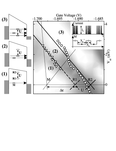
By measuring the differential conductance as a function of and we have been able to show directly that the increase of shot noise occurs in the region of - where two interacting impurities carry the current in a correlated way. Fig.3 presents the grey scale of the differential conductance plotted versus and . When a source-drain bias is applied, a single resonant impurity would give rise to two peaks in , which occur when the resonant level aligns with the Fermi levels . On the grey scale these peaks lie on two lines crossing at . Consider, for example, point in Fig.3. The central area between the lines corresponds to the impurity level between and , that is when the impurity is in its conducting state. Outside this region the impurity does not conduct, as it is either empty (on the left of the central region) or filled (on the right of it).
Experimentally, at small we see such a cross-like feature near point , with the left line being more pronounced. The exact positions of the maxima of the conductance peaks of this line are indicated by circles. It is seen that with increasing , a new parallel line appears at V and mV, shifted to the left by mV. The maxima of the conductance peaks of this line are shown by triangles.
In Fig.3 the modulator cross is plotted according to the analysis below - experimentally we cannot observe these lines because the modulator conductance peaks are too small, due to low leak rates and . The -line occurs in the inner region of the modulator cross, i.e. where the modulator occupancy changes in time. Therefore, lines and reflect the Coulomb shift of level : the former corresponds to the empty modulator and the latter - to the occupied one. The modulation of the current should then occur in region (2), Fig.3: the central part of cross between lines and , corresponding to diagram (2). As discussed before, in region (3) there is no modulation as both states and can conduct, and in region (1) there is no current as the low state is still above .
In Fig.4 current noise and the Fano factor are presented as functions of for different . It shows that indeed the increase of noise occurs only in region (2) in Fig.3. Namely, the increase of noise appears only between V and V, that is, in the central region of cross . In addition, when is swept at fixed , one can see that the hump in the Fano factor appears only between lines and .
In order to quantitatively compare the model with the experiment we have to take into account that in our experiment resonant tunnelling via state exists in parallel with the background hopping. Then the total Fano factor has to be expressed as , where , and , are the Fano factors and currents for RT and hopping, respectively. In order to get information about the background hopping we have measured noise at V, i.e. away from the RT peak under study in Fig.3. It has been estimated as . This value of the Fano factor is expected for shot noise in hopping through potential barriers (1-2 impurities in series) Roshko ; Korotkov!Likharev1D ). The bias dependence of the background current at this is also consistent with hopping current via two impurities: Glazman!Matveev .
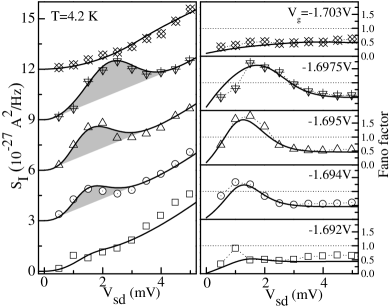
Assuming that the background current is approximately the same for all studied gate voltages, we have added up the contributions to the Fano factor from RT via two interacting impurities, and , and the background hopping. The numerical results have been fitted to the experimental and , Fig.4. The fitting parameters are the leak rates of and ( eV, eV, and eV, eV ), the energy difference between and ( meV), and the Fano factor for the background hopping (). The coefficients in the linear relation between the energy levels , and , have also been found to match both the experimental data in Fig.4 and the position of lines and in Fig.3. One can see that the model gives good agreement with the experiment. The Coulomb shift ( meV) found from Fig.3 agrees with the estimation for the Coulomb interaction between two impurities not screened by the metallic gate: meV, where Å is the distance between the gate and the conducting channel.
It is interesting to note that the hopping background effectively hampers the manifestation of the enhanced Fano factor , i.e. without the background the Fano factor enhancement would be much stronger. The largest experimental value of in Fig.4 (at V) is approximately , while a numerical value for RT at this is .
In conclusion, we have observed enhanced shot noise in resonant tunnelling via localised states in a short-barrier structure. We have demonstrated that this effect originates from Coulomb interaction between two localised states which imposes correlations between electron transfers. A simple model is shown to provide a quantitative description of the observed enhancement.
We are grateful to E.V. Sukhorukov for stimulating discussions, FOM, EPSRC and ORS fund for financial support.
References
- (1) Y.M. Blanter and M. Büttiker, Phys. Rep. 336, 2 (2000).
- (2) G.B. Lesovik, JETP Lett. 49 592 (1989); M. Büttiker, Phys. Rev. Lett. 65, 2901 (1990).
- (3) A.N. Korotkov, Phys. Rev. B 49,10381 (1994).
- (4) M. Reznikov et. al., Phys. Rev. Lett. 75, 3340 (1995); A. Kumar et. al., Phys. Rev. Lett. 76, 2778 (1996).
- (5) F. Liefrink et. al., Phys. Rev. B 49, 14 066 (1994); A.H. Steinbach, J.M. Martinis, and M.H. Devoret, Phys. Rev. Lett. 76, 3806 (1996); M. Henny et. al., Phys. Rev. B 59, 2871 (1999).
- (6) A.B. Fowler, G.L. Timp, J.J. Wainer, and R.A. Webb, Phys. Rev. Lett. 57, 138 (1986); T.E. Kopley, P.L. McEuen, and R.G. Wheeler, Phys. Rev. Lett. 61, 1654 (1988).
- (7) L.Y. Chen and C.S. Ting, Phys. Rev. B 46, 4714 (1992).
- (8) Y.V. Nazarov and J.J.R. Struben, Phys. Rev. B 53, 15466 (1996).
- (9) Y.P. Li et. al., Phys. Rev. B 41, 8388 (1990).
- (10) H. Birk et. al., Phys. Rev. Lett. 75, 1610 (1995).
- (11) V.V. Kuznetsov et. al., Phys. Rev. Lett. 85, 397 (2000)
- (12) S.H. Roshko et. al., Physica E 12, 861 (2001).
- (13) G. Iannaccone et. al., Phys. Rev. Lett. 80, 1054 (1998); Ya. M. Blanter and M. Buttiker, Phys. Rev. B 59, 10217 (1999).
- (14) M. J. Kirton and M. J. Uren, Adv. Phys. 38, 367 (1989).
- (15) A.N. Korotkov and K.K. Likharev, Phys. Rev. B 61, 15975 (2000).
- (16) L.I. Glazman and K.A. Matveev, Zh. Eksp. Teor. Fiz. 94, 332 (1988) [Sov. Phys. JETP 67, 1276 (1988)].
- (17) M. Eto, Jpn. J. Appl. Phys. 36, 4004 (1997).