Self-consistent Coulomb effects and charge distribution of quantum dot arrays
Abstract
This paper considers the self-consistent Coulomb interaction within arrays of self-assembled InAs quantum dots (QDs) which are embedded in a pn structure. Strong emphasis is being put on the statistical occupation of the electronic QD states which has to be solved self-consistently with the actual three-dimensional potential distribution. A model which is based on a Green’s function formalism including screening effects is used to calculate the interaction of QD carriers within an array of QDs, where screening due to the inhomogeneous bulk charge distribution is taken into acount. We apply our model to simulate capacitance-voltage (CV) characteristics of a pn structure with embedded QDs. Different size distributions of QDs and ensembles of spatially perodic and randomly distributed arrays of QDs are investigated.
pacs:
73.63.KvI Introduction
The strong localization of few electrons in three dimensions is one of the key features of quantum dots bim99 (QDs). This results in a variety of properties making them potential candidates for new semiconductor applications such as laser and memory devices gru00 ; fin98 ; yus97 . One of those properties is the singular density of states, which relies on the alignment of the energy levels in the whole QD ensemble. On the one hand this requires a fairly homogeneous QD size distribution, on the other hand the statistical occupation of electronic QD levels gru97 changes the energy of levels of the same dot and all neighboring QDs due to Coulomb interaction.
The amount of Coulomb repulsion between QD electrons, especially at different QDs, is expected to depend on the details of the complicated bulk charge distributions of the QD device. Additionally, the microscopic charging and discharging processes of the QDs depend on the energy differences between the QD levels and the non-equilibrium quasi-Fermi level, resulting in a very complicated self-consistent problem. The microscopic charge distribution in the QD array is never stationary due to the statistical character of microscopic processes, but for large ensembles of QDs or in a long time average a stationary mean QD sheet charge density is attained. Standard approaches use quasi one-dimensional models where the charge in the QDs is approximated by a homogeneous sheet charge bro98b ; bru99 . This is suitable to obtain the QD energy levels by a fit to experimental capacitance-voltage (CV) data wet00 , where a Gaussian distribution of QD energy levels was assumed. Nevertheless the interpretation of the fitted broadenings remains controversial, since they may result both from size fluctuations and inhomogeneous charging effects of the single QDs.
The model used in this work calculates self-consistently the charge distribution in an array of QDs, with respect to the three-dimensional potential distribution under bias conditions. From an ensemble average of many QD charge configurations, the mean stationary QD sheet charge is calculated, to obtain macroscopic quantities like the depletion capacitance and the CV characteristics. The use of the electrostatic Green’s function method makes this expensive self-consistent problem solvable and charging effects in the QD array can be investigated separately from structural fluctuations.
II Theory
Since only a small but essential part of the structure is not translationally invariant in the lateral (,) directions, but most of the device is inhomogeneous only in the growth direction () the problem of solving the three-dimensional non-linear Poisson’s equation is divided up into calculating two one-dimensional potentials and and a suitable 3D Green’s function. The potential is introduced as the self-consistent solution of the non-linear one-dimensional Poisson’s equation
| (1) |
and the current equations neglecting generation and recombination in the active region
| (2) |
where the QD charge is treated as a sheet charge (per unit area) averaged over the lateral directions. The bulk charge density is a function of the local potential , and the electron and hole quasi-Fermi levels and . The electron current and the hole current are calculated within a drift-diffusion model. Ohmic contacts are used to obtain boundary conditions for , and . For further details see Ref. wet00 . Here, and denote the absolute and relative permittivities of the semiconductor material, and is the characteristic function
| (3) | |||||
where is the height of the QDs, accounting for the localization in direction.
is the potential which is felt by a single QD charge, originating from the bulk charge if the QD charges would not exist. , where is the position of the QDs, can be conceived as a background potential for the QDs. is calculated as but without from eqn. (1).
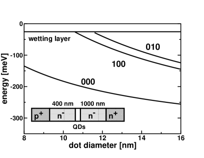
In this paper the intrinsic QD level energy of a state in QD (where , , are the respective quantum numbers) is measured from the conduction band edge. In order to specifically account for the size dependence of the level energies in InAs QDs we use a fit to the results of calculations sti99 as shown in Fig. 1.
The charging energy originating from the Coulomb interaction of the QD electrons is treated as a first order perturbation. Thus the QD electron energy can be expressed as
| (4) |
Here denotes the intrinsic conduction band edge, and is the elementary charge. The Coulomb charging energy can be expressed by the use of the capacitance matrix wha96 as
| (5) |
Here denotes the occupation numbers of the QD state in QD ( if occupied, if not occupied). ensures that an electron does not interact with itself. The charging energies obtained by summing over will be referred to as intradot charging energy, where the sum over is referred to as interdot charging energy in this paper. The elements of the inverse of the capacitance matrix can be expressed by the use of the Green’s function war98 :
| (6) |
Here and symbolize the QD electron wavefunctions. Assuming that the QD electrons are distributed homogeneously within cylinder shaped QDs with height and a diameter , neglecting the details of the QD wave functions leads to
| (7) |
where and denote the volumes of two QDs and . In our model the charging energies are the same for all states within a particular QD. A Green’s function including the static screening effects by free bulk charges can be found by defining a screening parameter as
| (8) |
Then is calculated as lan91
| (9) | |||
where is the Laplace operator and is the radial distance in the plane. The solution of eqn.(9) has a cylindrical symmetry, since and depend only on . Note that is the potential of a unit point-like charge positioned at , .
The QDs are occupied statistically according to the level energies and the contact quasi-Fermi level with the occupation probability
| (10) |
where is the temperature and denotes Boltzmann’s constant. Note that every change in the occupation numbers changes all QD level energies. The stationary, mean QD sheet charge density used in eqn. (1) is found as a charge configuration average
| (11) |
where denotes simulated realizations of configurations of occupied QD levels, and is the quadratic contact cross section simulated. Periodic boundary conditions are used in the four parallel and four diagonal directions in the QD plane. Since , which takes values from 1 m to 3 m in our simulations, is always larger than the maximum expected screening length for this structure, the influence of boundaries is negligible. In other words, a QD charge does not “see” itself in the periodically continued plane. The stationary depletion layer capacitance is determined as in Ref. wet00 by the electric field in the depletion layer given by .
III Results
The pn structure considered here consists of highly doped and GaAs contact regions, as well as a -doped GaAs region. A layer of self-organized InAs QDs is positioned 400 nm from the pn interface. The structure is displayed in the inset of Fig. 1. Similar pn structures have been investigated experimentally by CV spectroscopy and DLTS measurements kap99 ; kap00a . We simulate arrays of up to by QDs with a QD sheet density of for various temperatures and ensembles of QDs. The average QD diameter is 12 nm. A QD height of 3 nm is used.

III.1 Ideal dot distribution
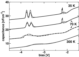
When a reverse bias is applied to the diode, bulk carriers as well as QD states will be successively discharged wet00 . First we simulate the structure at 4 K, 35 K, 70 K, 150 K and 300 K with periodically ordered QDs and with all QDs having the same size. The resulting CV characteristics are shown in Fig. 2. The main drop of the capacitance with increasing reverse bias is due to the increasing bulk depletion region sze81 . On top of this background three peaks can clearly be observed for temperatures less than 150 K. The peak at -2.2 V originates from the discharging of the excited states, which is split since piezoelectric fields break the degeneracy of the states (100) and (010) (see Fig. 1). At -3.6 V the two ground state electrons are discharged successively leading to a double peak. Here, the energy degeneracy is broken by the Coulomb charging effects. The Coulomb splitting has also been observed experimentally for different structures med97 ; med97a ; luy99 . The peak structure is broadened with rising temperature, resulting in a plateau in the CV characteristics at 300 K. Our calculations use a charging energy of about 20 meV. From the ground state peak splitting in the 4 K curve of about 100 mV we can estimate a lever-arm factor of 200 meV/V which, when applied to the width of the ground state peaks, results in an energy broadening of 2.5 meV. This value coincides with the unscreened Coulomb potential (in units of energy) of two electrons at a distance of 100 nm from a QD (2 1.25 meV). This means that the broadening at 4 K originates from the charge fluctuations within the four nearest neighbor QDs, in particular if every second one is charged. At 300 K, where occupation is rather insensitive to the QD level spacing, the full plateau width of about 500 mV corresponds to an energy broadening of 100 meV. This value can be attributed to the broadening in InAs QDs of the Fermi distribution function of about at 300 K of the two ground state levels. Consequently, at large temperatures, the charging energy is given by the averaged, statistically distributed charge stored in the QD array. This is the reason why the CV characteristics shows a flat plateau at 300 K and is hardly distinguishable from that of a quantum well wan96 .
Additionally, the ground state peaks show a shift to lower reverse bias for rising temperatures, where the excited states peaks do not show this feature. This shift can be explained as follows: When the ground states electrons are discharged, interdot charging energies become more important than for the excited states (explained later in detail). The interdot interaction depends on how the free electrons can screen the interdot Coulomb potential. This ability rises with lower temperatures leading to shorter screening lengths. Therefore the charging energies are lower at low temperatures, and a higher reverse bias has to be applied to discharge the ground state electrons.
III.2 Impact of structural fluctuations
Now we investigate the impact of structural fluctuations of the QD ensemble such as position disorder and size fluctuations. At first we distribute the equally sized QDs randomly instead of periodically in the lateral plane leaving the QD sheet density constant. Compared to the characteristics without fluctuations (solid lines in Fig. 3) at 35 K and 70 K the ground state peaks for randomly distributed QDs are only slightly smeared out (dashed lines in Fig. 3). Since the electrons in the excited states can be thermally activated more easily due to fluctuations in the interdot Coulomb interaction, resulting in an inhomogeneous charging of these levels, the respective peaks are more strongly broadened.
Next we simulate an ensemble of periodically ordered QDs with random QD diameters between 10 and 14 nm at 70 K, corresponding to a fluctuation of 17 %. The resulting CV characteristic (see dash-dotted line in Fig. 3) shows a very broad ground state peak. Again, the excited states are more sensitive to the fluctuations, i.e., the respective peak disappears almost completely. The increase of the fluctuations of the diameter to 33 % (8 - 16 nm) leads to a broad ground state plateau in the characteristics (dotted lines in Fig. 3). Such a plateau has been observed experimentally for similar pn structures kap99 ; kap00a , and a comparison with our results indicates that the size fluctuations in self-organized QDs is of this order of magnitude. This size fluctuation corresponds to an energy fluctuation of the ground state of about 100 meV (Fig. 1), which coincides with the typical value for the broadening of the ground state in the photoluminescence signal of InAs QDs kap99 . For room temperature the CV characteristics with 33 % size fluctuation shows almost no deviation from the characteristics without fluctuations. Here, thermal charge fluctuations dominate the behavior.
As already mentioned, the QDs are discharged by applying a reverse bias. In Fig. 4 the mean number of electrons per QD is displayed as a function of bias for 35 K, 70 K and 300 K. At 35 K and 70 K the QDs are charged with three electrons at zero bias and are discharged monotonically in a step-like manner at biases where peaks are observed in the CV characteristics (solid lines). Structural fluctuations lead to a broadening of these curves (dashed, dash-dotted and dotted lines). Additionally, with size fluctuations of 33 % some QDs can store up to four electrons, leading to a higher average QD occupation. For 300 K the QDs are charged with less electrons, because of the lower degree of degeneracy of bulk electrons in the contact region, and consequently the lower lying quasi-Fermi level at higher temperatures.

III.3 Variation of the charging energy
The mean charging energy per QD electron as shown in Fig. 5 shows an interesting, non-monotonic behavior. At 70 K without fluctuations (solid lines) the charging energy is at first constant for -0.5 V and then rises until the excited state electrons are rapidly discharged. Between =-2.2 V and =-3.6 V the charging energy again rises, and then drops to zero when the residual ground state electrons are discharged. The continuous increase of the charging energies can be explained by considering the bulk electrons in the vicinity of the QDs being depleted with reverse bias. This depletion increases the interdot charging energy, and therefore the total QD level energies. Fig. 5 shows that these negative and positive differential charging energies persist even for 33 % size fluctuations at 70 K. Also for 300 K this behavior can be observed, but it vanishes when taking into account additionally 33 % size fluctuations. The mean height of the potential barrier at the QD sheet as obtained from the one-dimensional Poisson’s equation is also displayed in Fig. 5. It shows the big difference of the charging energies between one-dimensional and three-dimensional calculations, especially if the QDs are charged with more than two electrons. But nevertheless, it shows the same differential behavior, which has an inhibitory effect on leakage and recombinations currents in QD devices, and therefore may provide an explanation for the observed bistabilities in similar pn structures kie03 .
To explain the origin of the negative differential charging energies in more detail, the charging energies are plotted in Fig. 6 as a function of bias, assuming that all QDs are charged with one electron at any bias and adding one extra electron into a single QD. We also differentiate between the intradot charging energy (solid line) originating from the second electron in a QD, and the interdot charging energy (dashed line) from the Coulomb repulsion with all neighboring QDs. The ratio of the Green’s function and the unscreened Green’s function () is also displayed in the two insets of Fig. 6 for =-1.5 V and =-4.5 V as a function of the lateral position and the vertical position as contour plots. As shown in Section II, the Green’s function determines the capacitance matrix and therefore the charging energies. As the Green’s function spreads out more and more, especially in the lateral directions, the charging energies due to interdot charging effects become larger. The effect on the intradot charging energy is rather small, since the size of the QDs is small compared to the distance of the free electron gas and the respective screening length. But by depletion of the free electrons with the applied reverse bias, the interdot charging rises. The slope of the interdot charging energy can clearly be identified with the slope of the mean charging energy of Fig. 5 for biases where the QD charge is constant but non-zero.


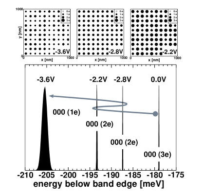
Fig. 7 shows the QD charge distribution within the QD layer for =-2.2 V, =-2.8 V and =-3.6 V and the energy distribution of the ground state (000) at =0.0 V, =-2.2 V, =-2.8 V and =-3.6 V for 70 K and without structural fluctuations. The normalizations of the distributions have been chosen differently for clarity. The QD charge distribution is inhomogeneous when the QDs are discharged at =-2.2 V and =-3.6 V, but it is homogeneous at =-2.8 V. Fig. 7 shows that the initial ground state energy at =0.0 V is lowered due to discharging one electron at -2.2 V. Then the energy rises (up to -2.8 V), due to the rising interdot charging energies as argued above. The discharging of the ground state electron then leads to a lowering of the QD electron energies again. Overall, the QD energy shows a zig-zag behavior when sweeping the bias.
The inhomogeneity of the QD charge leads also to a line broadening of the electron states. For =-2.8 V and =0.0 V the charge distribution is homogeneous, and the broadening vanishes. As shown above the magnitude of the Coulomb interaction between the QDs depends on the bias (Fig. 6). Therefore the line broadening at =-2.2 V is still small even for an inhomogeneous QD charge, since the interdot interaction is close to zero. The broadening becomes larger (about 2 meV) at =-3.6 V, since at this bias the charge distribution again is inhomogeneous, and the interdot interaction is large (see Fig. 6).
IV Conclusion
In conclusion, we have proposed a model to calculate the self-consistent three-dimensional charge distributions and charging energies within a QD device. We have shown that the charging energies depend on the electronic structure, which is determined by doping concentration, bias and temperature. The effects of size fluctuations of the dots and the role of a spatially periodic or random distribution of the dots on the capacitance-voltage characteristics have been investigated. We have found that size fluctuations have a much stronger influence on the broadening of the peak structure of the CV characteristics than the positional disorder of the QDs. Our detailed simulations have shown that the QD energy can be a strongly non-monotonic function of the applied bias.
Acknowledgement
This work was supported by DFG in the framework of Sfb 296. Helpful discussions with C. Kapteyn and R. Heitz are acknowledged.
References
- (1) D. Bimberg, M. Grundmann, and N. Ledentsov, Quantum Dot Heterostructures (John Wiley & Sons Ltd., New York, 1999).
- (2) M. Grundmann, Appl. Phys. Lett. 77, 4265 (2000).
- (3) J. J. Finley, M. Skalitz, M. Arzberger, A. Zrenner, G. Böhm, and G. Abstreiter, Appl. Phys. Lett. 73, 2618 (1998).
- (4) G. Yusa and H. Sakaki, Appl. Phys. Lett. 70, 345 (1997).
- (5) M. Grundmann and D. Bimberg, Phys. Rev. B 55, 9740 (1997).
- (6) P. N. Brounkov, A. Polimeni, S. T. Stoddart, M. Henini, L. Eaves, P. C. Main, A. R. Kovsh, Y. G. Musikhin, and S. G. Konnikov, Appl. Phys. Lett. 73, 1092 (1998).
- (7) P. N. Brunkov, A. R. Kovsh, V. M. Ustinov, Y. G. Musikhin, N. N. Ledentsov, S. G. Konnikov, A. Polimeni, A. Patane, P. C. Main, L. Eaves, and C. M. A. Kapteyn, Journal of Electronic Materials 28, 486 (1999).
- (8) R. Wetzler, C. M. A. Kapteyn, R. Heitz, A. Wacker, E. Schöll, and D. Bimberg, Appl. Phys. Lett. 77, 1671 (2000).
- (9) O. Stier, M. Grundmann, and D. Bimberg, Phys. Rev. B 59, 5688 (1999).
- (10) C. B. Whan, J. White, and T. P. Orlando, Appl. Phys. Lett. 68, 2996 (1996).
- (11) R. J. Warburton, B. T. Miller, C. S. Dürr, C. Bödefeld, K. Karrai, J. P. Kotthaus, G. Medeiros-Ribeiro, P. M. Petroff, and S. Huant, Phys. Rev. B 58, 16221 (1998).
- (12) P. T. Landsberg, Recombination in Semiconductors (Cambridge University Press, Cambridge, 1991).
- (13) C. M. A. Kapteyn, F. Heinrichsdorff, O. Stier, R. Heitz, M. Grundmann, N. D. Zakharov, D. Bimberg, and P. Werner, Phys. Rev. B 60, 14265 (1999).
- (14) C. M. A. Kapteyn, M. Lion, R. Heitz, D. Bimberg, P. Brunkov, B. Volovik, S. Konnikov, A. Kovsh, and V. Ustinov, Appl. Phys. Lett. 76, 1573 (2000).
- (15) S. M. Sze, Physics of Semiconductor Devices (Wiley, New York, 1981).
- (16) G. Medeiros-Ribeiro, F. G. Pikus, P. M. Petroff, and A. L. Efros, Phys. Rev. B 55, 1568 (1997).
- (17) G. Medeiros-Ribeiro, J. M. Garcia, and P. M. Petroff, Phys. Rev. B 56, 3609 (1997).
- (18) R. J. Luyken, A. Lorke, A. O. Govorov, J. P. Kotthaus, G. Medeiros-Ribeiro, and P. M. Petroff, Appl. Phys. Lett. 74, 2486 (1999).
- (19) J. B. Wang, F. Lu, S. K. Zhang, B. Zhang, D. W. Gong, H. H. Sun, and X. Wang, Phys. Rev. B 54, 7979 (1996).
- (20) G. Kießlich, A. Wacker, E. Schöll, S. A. Vitusevich, A. Förster, N. Klein, A. E. Belyaev, L. Eaves, P. Main, M. Henini, and S. V. Danylyuk, submitted to Phys. Rev. B (unpublished).