Institut für Theoretische Physik, Universität Regensburg, D-93040 Regensburg, Germany
Electronic transport in mesoscopic or nanoscale materials Molecular electronic devices Electronic structure of nanoscale materials; nanoscale contacts
Conductance of a molecular junction mediated by unconventional metal-induced gap states
Abstract
The conductance of a molecular junction is commonly determined by either charge-transfer-doping, where alignment of the Fermi energy to the molecular levels is achieved, or tunnelling through the tails of molecular resonances within the highest-occupied and lowest-unoccupied molecular-orbital gap. Here, we present an alternative mechanism where electron transport is dominated by electrode surface states. They give rise to metallization of the molecular bridge and additional, pronounced conductance resonances allowing for substantial tailoring of its electronic properties via, e.g. a gate voltage. This is demonstrated in a field-effect geometry of a fullerene-bridge between two metallic carbon nanotubes.
pacs:
73.63.-bpacs:
85.65.+hpacs:
73.22.-fMolecular electronics has recently received increased attention owing to the realization of active device components based on single-molecule conductors at either low or room temperature. These range from rectifiers, negative-differential-resistance switches and electromechanical amplifiers to single-electron devices, nanomechanical oscillators and field-effect transistors [1]. Such achievements have been complemented by advances in the theory of electron transport across molecular junctions to include both non-trivial quantum mechanical effects at this scale [2] (cf tunnelling and interference) and the electronic structure of the components involved [3, 4, 5, 6, 7, 8, 9]. Although some experimental aspects remain controversial, detailed studies of current-voltage curves (I-Vs) at either the semi-empirical or first-principles level have accumulated evidence of what determines the electronic response of an electrode–molecule–electrode setup. The most important factors include the molecular electronic structure [4], band lineup and potential profile [5], structural conformations [6, 9], charging effects [7], and the electron-phonon coupling in low-conduction molecular wires [8]. Their respective action crucially depends on the realised interface.
In this Letter we discuss an important interfacial effect on the properties of the molecular junction. Namely, we present an unconventional way to metallization of a molecular-bridge, which owes to states localized on the surface of the electrodes rather than to their bulk Bloch states. They introduce prominent conductance resonances within the HOMO-LUMO gap of the isolated molecule in close alignment to EF, in addition to the usual broadening of the molecular levels by the metal-induced gap states (MIGS) [10]. Their tuning by a gate voltage may be used to realize a molecular switch in a field-effect geometry.
Surface resonant states of electrodes are also important to scanning-tunnelling-microscope (STM) images obtained by sharp tips [11], often employed in single-molecule transport measurements [1, 3]. However, such states are commonly missing from conventional models of molecular junctions. These usually involve the atomistic simulation of electrodes with bulk or seamless properties, and the employment of idealised jellium leads [3, 4, 5, 6, 7, 8].
For definitiveness, we study the transport properties of an all-carbon molecular device consisting of a carbon nanotube (CNT)-\chemC_60 hybrid system with closed end CNT surfaces. The implications of our results and experimental realizations are discussed later on. Electron transport across the molecular junction is studied in the Landauer formalism [2] by using numerical Green function techniques combined with a tractable electronic-structure tight-binding approach parametrized by density functional theory (DFT) [12]. The two-terminal conductance as calculated by is a function of the energy of injected electrons from the electrodes. is the transmission function, which within the Landauer picture relates the conductance of the system to an independent-electron scattering problem. The factor two implies spin-degeneracy.
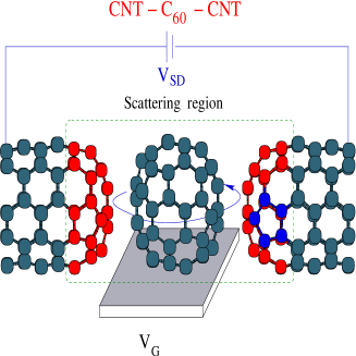
We present the CNT–fullerene device-setup in Fig. 1. We consider a \chemC_60 molecule between two semi-infinite metallic CNTs. The diameters of the considered armchair- CNTs and the fullerene are comparable (nm). In particular, a CNT is terminated by a cap with the shape of half a \chemC_60 molecule positioned so that the nanotube axis crosses vertically a single pentagon at its centre. The CNTs are aligned mirror-symmetrically to a single-axis. The centre of the fullerene is placed at the mid-point between the two pentagons at the cap-edges. Although both the \chemC_60 and the capped CNTs have appreciable stability, we perform additional structural optimization in the depicted scattering region of Fig. 1 to include any conformational changes due to the proximity of the two subsystems. Mainly, the \chemC_60 is compressed along the transport direction taking an ellipsoidal shape. For a device placed on a substrate the optimization details depend on the substrate choice and deserve a systematic study. Our main conclusions remain unaffected, if a rather passive substrate is assumed. For example, the surface van der Waals forces on CNTs deposited on the H-passivated Si(100) modifies their shape and electronic properties only if the diameter exceeds nm [13].
We emphasize three features of our system: (i) it consists purely of carbon atoms, (ii) the lateral dimension of the electrodes is at the nanoscale, and most importantly, (iii) the surface of the electrodes, i.e, the caps, possess unambiguous localised states with energies near the equilibrium Fermi energy. The latter have been predicted in Ref. [14] and after experimental observation [15] thoroughly studied for their field-emission properties. All the above points have important implications for possible applications. In anticipation of our results, the fulfillment of (iii) for an electrode is a necessary condition for the presence of unconventional MIGS in the molecular bridge.
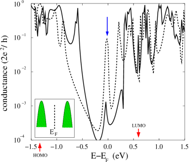
It is instructive to first examine typical spectra of the Landauer conductance for two possible orientations of \chemC_60 with respect to the CNTs. In Fig. 2, the sensitivity of electron transport on the geometry of the CNT electrodes–\chemC_60 interface is shown. Similar to the results of our previous study [9] of the conductance as a function of the relative orientation in an open end CNTs-\chemC_60 hybrid, conductance variations up to two orders of magnitude are found. The strong dependence on orientation derives from the interplay between direct change of the magnitude of tight-binding coupling parameters [16] and more subtle effects reflecting the exact atomic-contact geometry [17]. The latter include interference at the atomic level and are typically enhanced at molecular junctions with mesoscopic electrodes (see point (ii) above).
Detailed underlying effects are better demonstrated in simpler setups by assuming only one molecular site coupled to each electrode [17]. However, a hint is given by writing
| (1) |
is the retarded(advanced) molecular Green function including a self-energy interaction (left, L, and right,R, lead) with the electrodes. The matrices are defined via
| (2) |
| (3) |
with the coupling matrix of \chemC_60 to the CNTs and the retarted Green function of the CNTs. In our basis, contains the DFT parametrised tight-binding matrix elements. Rows of couple molecular sites to more than one CNT-site bringing in interference terms.
However, and in strong contrast to Ref. [9], our central result relates to the marked peak in both curves of Fig. 2. Whereas the peak-height evidently fluctuates strongly, its relatively large width (eV) compared to room temperature and its adjacent position to the Fermi energy prevail for a large number of possible orientations that we have investigated. This suggests an effective means to control the electronic properties of the device (see below). We will now analyse the origin of these states.

If no significant charge transfer occurs between a molecular bridge and the electrodes, which could pin EF to one of the molecular resonances, then electron transport proceeds by tunnelling through the HOMO-LUMO gap as indicated in the inset of Fig. 2. Such band lineup is typical for metal–semiconductor interfaces leading to a Schottky barrier. Otherwise, if charge transfer shifts the position of the molecular resonances, the conductance around EF would look similar to Fig. 2, which would point to resonant tunnelling via a molecular orbital. This would however lead to a misinterpretation of our results. As inferred by the pure-carbon structure (point (i) above), we can safely exclude the possibility of large charge-transfer-doping at equilibrium conditions in the present set-up. This is further supplemented by Mulliken population analysis showing a small accumulation of charge on \chemC_60 (). Note aditionally that by the position of the HOMO and LUMO of the isolated \chemC_60 alone, we cannot conclude to which molecular resonance, if any, the peak at EF corresponds. After contact to the electrodes the broadened molecular levels undergo positional shifts. This effect is enhanced by the multifold degeneracy of the HOMO (5-fold) and LUMO (3-fold). For the above reasons we argue that the observed peak is a manifestation of resonant states of the CNT caps, which lie within the HOMO-LUMO gap.
To further test the nature of the observed conductance resonance in the vicinity of Ef we have examined the local DOS. It is interesting to note that in a simple setup the transmission function reduces to the familiar formula , where is the local DOS at a cap-site [17]. In Fig. 3, we plot the local DOS per site, , where N is the number of atomic sites over which the trace is taken. The overlap matrix reflects the non-orthogonality of our basis. For the depicted in Fig. 1 the average is taken over the scattering region and one CNT unit cell on each side for two possible junctions. One setup is that of Fig. 1. In the other, the \chemC_60 molecular bridge has been removed. The appearance of the peak around the Fermi energy in both curves suggests that the conductance resonance in discussion corresponds to a cap state and not to a molecular orbital. We note that the bulk DOS of a metallic CNT shows a plateau in this spectral window.
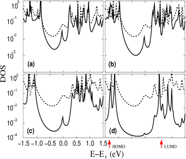
It is evident that even when the conductance is dominated by the cap states, electron transport should be supported by the molecular bridge. Namely, the wavefunction of the cap resonances must have noticeable amplitude on the molecule via evanescent penetration, in a similar fashion to through-bond tunnelling of Bloch states of the electrodes. Hence, the DOS of the fullerene should not only be finite but also show a similar peak. That is indeed the case as shown in Fig. 4. When increasing the distance between the electrodes in the setup of Fig. 1 the DOS of the \chemC_60 resembles that of its slightly perturbed spectrum. Both the small weight of the \chemC_60 DOS-peak at EF and its gradual reduction without any appreciable shift point again to the fact that it cannot be associated to either a HOMO or LUMO.
Having established the origin of the conductance resonance adjacent to EF and the role of the \chemC_60 molecular bridge as a through-bond mediator, one may utilise the latter to efficiently control the conductance of such a molecular device. Rotation of the \chemC_60 as implied by Fig. 2, and previously suggested [9], or other mechanical manipulation such as the demonstrated compression by an STM tip may be applied [3]. However, the resonant position with respect to EF makes the application of a gate potential Vg readily accessible. This probe may be provided by a third CNT [18] or a gated STM tip [19].
An external electric field modifies the charge-density inside the molecular region, and, hence, the electronic coupling across the molecular junction. We apply a crude approximation just to validate its effect on transport properties by rigidly shifting the \chemC_60 spectrum by the gate voltage. In Fig. 5, both the transmission function at EF and the current via for source-drain voltage V are plotted as a function of Vg. Manifestation of effective molecular switching is apparent.

Because of strong coupling between the \chemC_60 and the electrodes, as indicated by the finite molecular spectrum in Fig. 4 at all energies, no Coulomb blockade-related effects are expected. Electron interactions are registered only through the exact charging of the molecule via the electrostatic potential profile determined in a self-consistent manner. As we mentioned, in our system this defines nothing more than the details of electronic response when a gate-voltage is applied, also at moderate source-drain voltages (eV).
The suggested design not only serves as a definite example of unconventional molecular metallisation, but it is also of interest to the search for new-type all-carbon molecular devices. For example, much success has been made in realizing either single-fullerene or CNT devices. But unlike Fig. 1 in most experiments contact is made with common bulk metals. In order to take full advantage of molecular electronics prospects both the active region and the wiring elements should be at the molecular scale. At present this role is reserved for CNTs, also in our setup. Experiments already include I-V measurements of a carbon nanotube ring and a DNA molecule in an STM setup [18]. In those, CNTs are used for STM manipulation and simultaneously provide source/drain reservoirs and a gate terminal. More recently, interconnected CNTs by molecular linkers have been reported [20].
In conclusion, we have employed a novel molecular device to point out the existence of an alternative conduction mechanism in molecular junctions via unconventional metal-induced gap states. The latter owe exclusively to resonant states of the electrode contacting-interface and contrast the adopted view that electron transport across molecular junctions is simply dominated by hybridisation of the molecular orbitals. Such metallization is generic to the appearance of surface resonant states within the HOMO-LUMO gap. Switching behaviour under a gate voltage was demonstrated in this device. Moreover, anchoring groups of the molecular bridge may possess such states. One should further address their exact properties in the environment of a molecular junction together with their fingerprints on transport. Thus, we hope that the possibility to effectively tailor the electronic response of such setups will stimulate experiments and closer ties of molecular electronics to surface science.
Acknowledgements.
This study was supported by the Deutsche Forschungsgemeinschaft through the Forschergruppe “Nanostrukturierte Funktionselemente in makroskopischen Systemen”. GF is grateful to the Alexander von Humboldt foundation.References
- [1] Aviram A., Ratner M. and Mujica V. (Editors), Molecular Electronics II, Ann. N.Y. Acad. Sci. 960 (2002); Joachim C., Gimzewski J. K. and Aviram A., Nature (London), 408 (2000) 541; for a recent account see: Hänggi P., Ratner M. and Yaliraki S. N. (Editors), Special Issue of Chem. Phys. 281 (2002).
- [2] Datta S., Electronic Transport in Mesoscopic Systems (Cambridge University Press, Cambridge, 1995).
- [3] Joachim C., Gimzewski J. K. and Tang H., Phys. Rev. B, 58 (1998) 16407.
- [4] Emberly E. G. and Kirczenow G., Phys. Rev. B , 60 (1999) 6028; Di Ventra M., Pantelides S. T. and Lang N. D., Phys. Rev. Lett., 84 (2000) 979.
- [5] Datta S., Weidong T., Hong S. et al Phys. Rev. Lett., 79 (1997) 2530; Yaliraki S. N., Roitberg A. E., Gonzalez C. et al, J. Chem. Phys., 111 (1999) 6997; Xue Y., Datta S., and Ratner M. A., J. Chem. Phys., 115 (2001) 4292; Nitzan A., Galperin M., Ingold G.-L. and Grabert H., to appear in J. Chem. Phys..
- [6] Samanta M. P., Tian W., Datta S. et al, Phys. Rev. B, 53 (1996) R7626.
- [7] Lang N. D. and Avouris Ph., Phys. Rev. Lett., 84 (2000) 358; Taylor J., Guo H. and Wang J., Phys. Rev. B, 63 (2001) 121104(R); Lehmann J., Ingold G.-L. and Hänggi P., Chem. Phys. 281, (2002) 199.
- [8] Ness H. and Fisher A. J., Phys. Rev. Lett., 83 (1999) 452.
- [9] Gutierrez R., Fagas G., Cuniberti G. et al, Phys. Rev. B, 65 (2002) 113410.
- [10] For MIGS in bulk semiconductors see: Heine V., Phys. Rev., 138 (1965) A1689; Louie S. G. and Cohen M., Phys. Rev. B, 13 (1976) 2461; for MIGS in nanowires see: Landman U., Barnett R. N., Scherbakov A. G., Avouris Ph., Phys. Rev. Lett., 85 (2000) 1958; Tomfohr J. K. and Sankey O. F., Phys. Rev. B, 65 (2002) 245105.
- [11] Vázquez de Parga A. L., Hernán O. S., Miranda R. et al, Phys. Rev. Lett., 80 (1998) 357, and refs therein.
- [12] A DFT parametrization of nonorthogonal linear combination of (valence) atomic orbitals is used, see e.g. Gutierrez R., Grossmann F., Knospe O. and Schmidt R., Phys. Rev. A, 64 (2001) 013202, and refs therein.
- [13] Hertel T., Walkup R. E., and Avouris Ph., Phys. Rev. B 58, (1998) 13870.
- [14] Tamura R. and Tsukada M., Phys. Rev. B, 52 (1995) 6015.
- [15] Carroll D. L., Redlich P., Ajayan P. M. et al, Phys. Rev. Lett., 78 (1997) 2811.
- [16] Kornilovitch P. E. and Bratkovsky A. M., Phys. Rev. B, 64 (2001) 195413.
- [17] Fagas G., Cuniberti G. and Richter K., Phys. Rev. B, 63 (2001) 045416; Cuniberti G., Fagas G. and Richter K., Chem. Phys., 281 (2002) 465; Latgé A., Marcucci D. C. and Tovar Costa M. V., Physica E, 13 (2002) 1264.
- [18] Watanabe H., Manabe C., Shigematsu T. et al, Appl. Phys. Lett., 78 (2001) 2928; 79 (2001) 2462.
- [19] Gurevich L., Canali L. and Kouwenhoven L. P., Appl. Phys. Lett., 76 (2000) 384.
- [20] Chiu P. W., Duesberg G. S., Dettlaff-Weglikowska U. and Roth S., Appl. Phys. Lett., 80 (2002) 3811; there, interesting geometric effects arise [17].