Resistivity of dilute 2D electrons in an undoped GaAs heterostructure
Abstract
We report resistivity measurements from 0.03 K to 10 K in a dilute high mobility 2D electron system. Using an undoped GaAs/AlGaAs heterojunction in a gated field-effect transistor geometry, a wide range of densities, to , are explored. For high densities, the results are quantitatively shown to be due to scattering by acoustic phonons and impurities. In an intermediate range of densities, a peak in the resistivity is observed for temperatures below 1 K. This non-monotonic resistivity can be understood by considering the known scattering mechanisms of phonons, bulk and interface ionized impurities. Still lower densities appear insulating to the lowest temperature measured.
pacs:
71.30.+h, 73.40.-c, 73.50.BkThe resistivity of 2D electrons at zero magnetic field has been used to probe scattering and quantum processes for many years. Interest in the conducting behavior of 2D electrons and holes was further heightened in 1994 when Kravchenko and coworkers discovered an apparent metal-insulator transition of 2D electrons in Si MOSFETsmetal:si . While 2D systems are expected to exhibit insulating behavior (weak or strong localization) at sufficiently low temperatures and/or densities, the metallic side of the metal-insulator transition is more puzzling. A true metal conducts at , however here we use the term “metallic” as referring to at low temperature, where is the resistivity. Metallic behavior has been seen in a number of different material systems, including electrons in Si MOSFETsmetal:si , holes in GaAsmetal:pgaas1 ; metal:pgaas2 ; metal:pgaas3 and electrons in GaAsmetal:ngaas1 ; metal:ngaas2 provided the carrier density is reasonably low (but not so low that the system is in the insulating phase) and the mobility relatively high. While all of these experimental systems exhibit metallic behavior in certain regimes of density () and temperature, the quantitative behavior varies widely. As the temperature is lowered, can decrease by a factor of 10 in Si MOSFETsmetal:si compared to only a few percent for electrons in GaAsmetal:ngaas1 . The drop in resistivity is typically observed when the dimensionless parameter (ratio of Coulomb to kinetic energy, ) is much larger than 1, suggesting that electron-electron interactions may be important. The issue here is understanding the physical mechanisms underlying the metallic behavior and elucidating the roles of disorder and interaction.
In this Letter, we present the temperature dependence of the resistivity of a dilute 2D electron gas (2DEG) in GaAs. Electron-electron interactions can be extremely important in this system at low temperatures due to the low amount of disorder present in GaAs heterostructures. In the sample discussed here, the density can be continuously tuned from cm-2 () to cm-2 (). With the ability to achieve very high in low disorder samples, these resistivity measurements provide a test of the importance of Coulomb interactions in the metallic regime. In particular, the () values of our 2DEGs are very comparable to those in the best Si MOSFETs whereas the effective disorder in our sample (as measured by , is the Fermi wavevector and the mean free path) is more than two orders of magnitude lower. Earlier experimental studies of the metallic behavior in 2D electrons in GaAs systems were restricted to higher densities and lower mobilities, and the drop in resistivity was much weaker than the 20% drop observed here. Finally, the wide range of and reported here allow several scattering regimes to be identified.
We find that our measured temperature dependence of the resistivity can be qualitatively well understood solely within the framework of Fermi liquid theory. At high density, the resistivity is linear with temperature, and the slope agrees both with previous measurementsphonons:exp1 ; phonons:exp2 and established theory for acoustic phonon scatteringphonons:sds . For intermediate densities a low temperature peak in the resistance is observed. The non-monotonic resistivity agrees qualitatively with the predicted temperature dependence of ionized impurity scattering (screening at low and the transition from a degenerate Fermi gas to a classical system at high ).
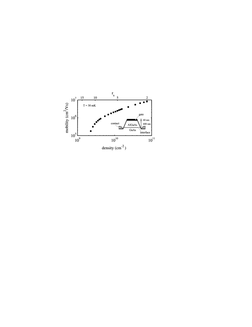
The sample used in this study is a high mobility 2DEG confined at the interface of a GaAs/Al0.3Ga0.7As heterojunction. The interface (see Fig. 1 inset) is separated by undoped AlGaAs from a bulk doped GaAs cap that serves as an integrated top gate. A mm2 square with 16 NiGeAu ohmic contacts is fabricated in a field-effect transistor geometrykane . The ohmic contacts are self-aligned to the top gate, and carriers are drawn into the channel by applying voltage between the gate and contacts. Once present, the density of the 2DEG is linearly proportional to the gate voltage. A calibration of the density is determined using Shubnikov-de Haas oscillations for a number of gate voltages. Although using undoped heterostructures requires complicated processing, an ultra-low density can be achieved without the penalty of a substantial fixed disorder potential arising from remote delta-doping.
The mobility, , is determined at mK where we empirically observe that the resistivity no longer changes with temperature. The mobility is extremely high throughout the entire density range, as is shown in Fig. 1. At the highest density for this sample the mobility is cm2/Vs (). In other devices that operate at higher density, we have measured a mobility of cm2/Vs at a density of cm-2, a value to which the data in Fig. 1 extrapolate. Since the mobility continues to increase at high density, interface roughness scattering is not relevant for data presented hereir_scattering .
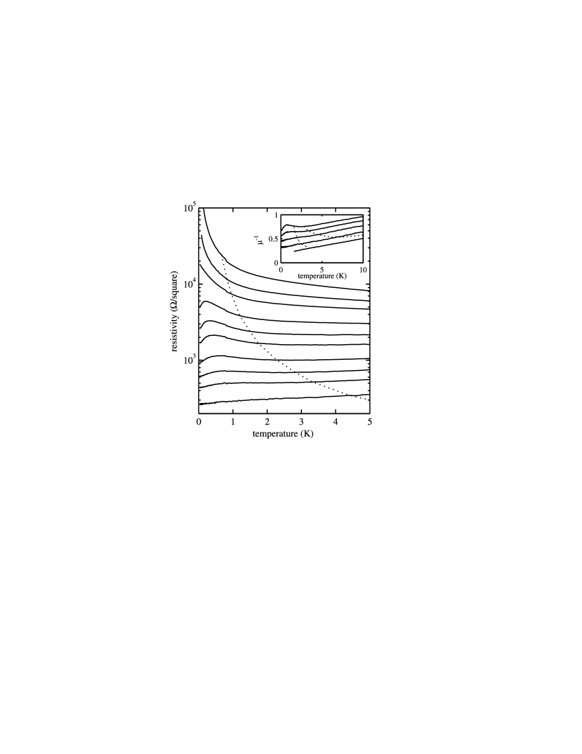
The temperature dependence of the resistivity for a number of different densities is shown in Fig. 2. The locus of Fermi temperatures is indicated with a dotted line. Three regimes can be identified. First, at high density ( cm-2) the resistivity is constant at low temperature and then increases as increases. For intermediate densities ( to ) the resistivity is non-monotonic with temperature. As increases, is initially constant (see Fig. 3), then increases and decreases to form a local maximum below K. The third regime occurs at the lowest densities, with the resistivity decreasing as the temperature increases in the experimentally accessible temperature range.
The phonon contribution to the resistivity at high density is better shown in the inset of Fig. 2, where is plotted for to cm-2. The inverse mobility for K is linear, and each density has roughly the same slope of Vs/Kcm2). Acoustic phonon scattering with both piezoelectric and deformation potential coupling leads to a linear dependence of above the Bloch-Grüneisen temperature (, is the phonon speed of sound). Previously reported experimentalphonons:exp1 ; phonons:exp2 and theoreticalphonons:sds studies of higher density 2DEGs in conventional GaAs heterostructures quantitatively agree with slope found here. This demonstrates that the resistivity of the high density 2DEG is accurately captured using well known scattering mechanisms. Note that the high temperature resistivity of the low density data in the inset of Fig. 2 remains consistent with phonon scattering even as the non-monotonic features begin to appear at low temperatures.
As the density is lowered below cm-2, the resistivity becomes non-monotonic. A peak in appears for , and the position of the peak shifts to lower temperature for lower densities. The resistivity at the maximum can be up to 23% larger than the low temperature ( mK) value of the resistivity. The non-monotonic peak occurs for , where phonon scattering is strongly suppressed. In this regime of and the temperature dependence of ionized impurity scattering must be considered. Screening leads to for sds_ionized , and the crossover from a degenerate Fermi gas to a classical system leads to for sds_ionized . Competition between these effects will lead to a low resistivity peak. Detailed calculations including both ionized impurity and acoustic phonon scattering are presented below (Fig. 4).
For the lowest density that can be attained in our samples decreases monotonically as increases. While it appears that the 2D electron system is insulating for these densities, comparison to the non-monotonic resistivities indicates a different interpretation is possible. Clearly, if the data were only taken to 0.2 K, some of the non-monotonic curves at higher density would also appear insulating. Similarly, it is possible that the low insulating behavior could become non-monotonic if the electron temperature were lowered further. From the results in Fig. 2, it is clear that a separatrix cannot be identified in this system. The functional form of the “insulating” temperature dependence for is more consistent with a power law dependence than an activated or Mott variable range hopping behavior.
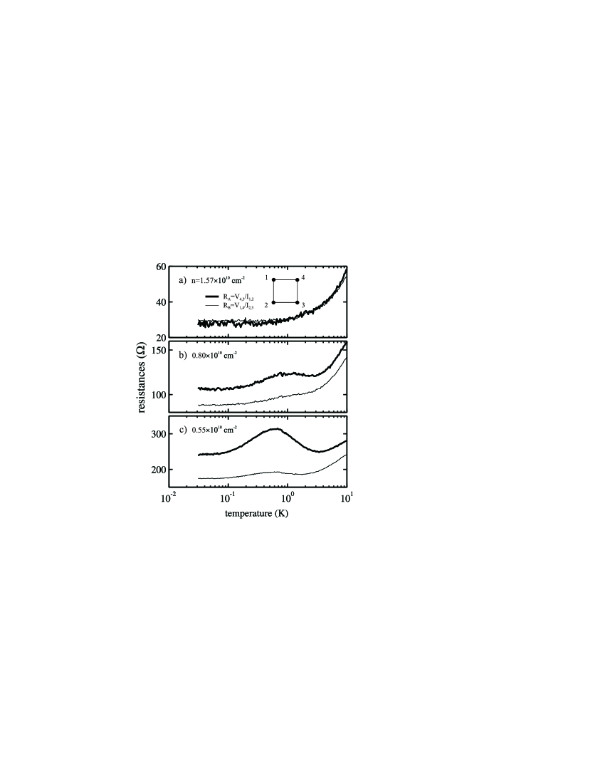
In performing measurements at low great care must be taken to insure that features do not arise as a result of inhomogeneities in the current flow. The temperature dependence of the resistances is shown in Fig. 3. Two resistances, and , are measured for current flowing, on average, in orthogonal directions. A constant current of 0.3 nA (for the lowest density) to 20 nA (for the highest density) is used in a standard lock-in amplifier measurement at a frequency of 7 Hz. At these currents, transport measurements (e.g. quantum Hall minima) indicate that the electrons cool below 50 mK. The resistivity is determined from the resistances using a procedure prescribed by Van der Pauwvdp . At high density ( cm-2, Fig. 3a), the curves and almost lie on top of each other and the temperature dependence is due to phonon scattering. At lower density (Fig. 3b,c), non-monotonic features appear in both and , but the resistances are no longer identical. Here we observe can be as large as 1.6. Earlier designs of undoped samples exhibited a severe ratio; approached 30. This effect originates in the sample fabrication, with the higher resistance always related to the location of the metallic gate contact. We speculate that the gate contact created a locally strained region above the square 2DEG causing inhomogeneous current flow. After redesigning the sample geometry to make the gate contact far from the square measurement region, was reduced by more than a factor of 10. While this effect is still visible in Fig. 3b and c, the remaining ratio has a very small ( 10%) impact on the resistivityvdp . Both and are non-monotonic, with resistance peaks located at nearly the same temperature. The qualitative nature of the non-monotonic resistivity is due to the underlying physics of ionized impurity scattering and not inhomogeneous current flow.
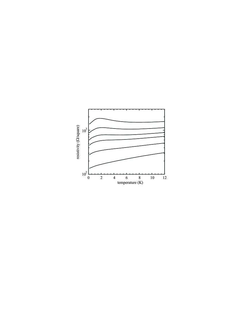
To understand the low temperature ( K) data, where the phonons contribute little to the resistivity as the system enters the Bloch-Grüneisen regime, we have carried out a microscopic transport calculation using the Boltzmann theory, where we include effects of charged impurity scattering on the electronic resistivity. Our calculation includes the following effects: (1) scattering by ionized charged impurities in the bulk GaAs layer and at the GaAs/AlGaAs interface; (2) temperature dependent screening, where the electron-charged impurity scattering is taken to be the temperature dependent statically screened Coulomb interaction with the screening calculated within the finite wavevector random phase approximation; (3) acoustic phonon scattering including both deformation potential and piezoelectric coupling; (4) the quasi-2D nature of the system through subband form-factors calculated in the Fang-Howard-Stern variational scheme. This approach is valid for .
We show our calculated results in Fig. 4 for several experimental intermediate and high densities. Reasonable values are chosen for bulk and interface impurities to allow a comparison of the calculated results to the experimental data shown in Fig. 2. Note that the overall resistivity scale depends on the unknown impurity densities, but the qualitative trends in are real and arise from very basic aspects of the underlying scattering mechanisms. The rise in with increasing at low temperatures is a direct effect of the thermal weakening of screening. The non-monotonicity of at the intermediate temperatures arises from the competition among temperature dependent screening, quantum-classical crossover and phonon scattering. The rise at higher is a phonon effect.
Quantitative understanding requires a more sophisticated theory which includes higher order electron-electron interactions and disorder induced localization corrections. Recently, electron-electron interaction corrections have been considered by Zala and coworkerszala . They find that for a range of temperature, where is the transport relaxation time, is expected to be linear. From the slope, the Fermi liquid parameter can be determined. In the data presented here there is no significant range over which linear is observed for (except for the phonon effect at higher ), and therefore we do not attempt to determine .
In conclusion, we have made resistivity measurements on low disorder gatable 2DEGs over a wide range of densities and temperatures. The resistivity data of high density 2DEGs agree quantitatively with both experimental and theoretical accounts of acoustic phonon scattering in GaAs. For the lowest densities, insulating behavior is observed. At intermediate densities, the resistivity becomes non-monotonic, with a peak appearing for . At low temperature the competition between screening () and a crossover from a degenerate Fermi system to a classical 2D gas () leads to the formation of a peak. Theoretical scattering calculations including both ionized impurities and acoustic phonons in GaAs show excellent qualitative agreement with the data. This agreement between experiment and theory suggests that the underlying physics involved is conventional Fermi liquid physics.
We acknowledge outstanding technical assistance from W. Baca and R. Dunn. This work has been supported by the Division of Materials Sciences and Engineering, Office of Basic Energy Sciences, US Department of Energy. Sandia is a multiprogram laboratory operated by Sandia Corporation, a Lockheed Martin Company, for the United States Department of Energy under contract DE-AC04-94AL85000.
References
- (1) S. V. Kravchenko, G. V. Kravchenko, J. E. Furneaux, V. M. Pudalov, and M. D’Iorio, Phys. Rev. B 50, 8039 (1994).
- (2) Y. Hanein, U. Meirav, D. Shahar, C. C. Li, D. C. Tsui, and H. Shtrikman, Phys. Rev. Lett. 80, 1288 (1998).
- (3) J. Yoon, C. C. Li, D. Shahar, D. C. Tsui and M. Shayegan, Phys. Rev. Lett. 82, 1744 (1999); H. Noh, M. P. Lilly, D. C. Tsui, J. A. Simmons, L. N. Pfeiffer and K. W. West, preprint, cond-mat/0206519.
- (4) A. P. Mills, Jr., A. P. Ramirez, L. N. Pfeiffer and K. W. West, Phys. Rev. Lett. 83, 2805 (1999).
- (5) Y. Hanein, D. Shahar, J. Yoon, C. C. Li, D. C. Tsui, and H. Shtrikman, Phys. Rev. B 58, 13338 (1998).
- (6) C. E. Yasin, M. Y. Simmons, A. R. Hamilton, N. E. Lumpkin, R. G. Clarke, L. N. Pfeiffer, and K. W. West, preprint, cont-mat/0204519.
- (7) H. L. Stormer, L. N. Pfeiffer, K. W. Baldwin and K. W. West, Phys. Rev. B 41, 1278 (1990).
- (8) J. J. Harris, C. T. Foxon, D. Hilton, J. Hewett, C. Roberts and S. Auzoux, Surf. Sci. 229, 113 (1990).
- (9) T. Kawamura and S. Das Sarma, Phys. Rev. B 42, 3725 (1990); Phys. Rev. B 45, 3612 (1992).
- (10) B. E. Kane, L. N. Pfeiffer, K. W. West, and C. K. Harnett, Appl. Phys. Lett. 63, 2132 (1993).
- (11) J. Heremans, M. B. Santos, K. Hirakawa, and M. Shayegan, J. Appl. Phys. 76, 1980 (1994).
- (12) S. Das Sarma and E. H. Hwang, Phys. Rev. Lett. 83, 164 (1999).
- (13) L. J. van der Pauw, Philips Res. Reports 13, 1 (1958).
- (14) G. Zala, B. N. Narozhny and I. L. Aleiner, Phys. Rev. B 64, 214204 (2001).