Giant Planar Hall Effect in Epitaxial (Ga,Mn)As Devices
Abstract
Large Hall resistance jumps are observed in microdevices patterned from epitaxial (Ga,Mn)As layers when subjected to a swept, in-plane magnetic field. This giant planar Hall effect is four orders of magnitude greater than previously observed in metallic ferromagnets. This enables extremely sensitive measurements of the angle-dependent magnetic properties of (Ga,Mn)As. The magnetic anisotropy fields deduced from these measurements are compared with theoretical predictions.
pacs:
75.60-d, 75.70.-i, 72.80.Ey, 75.50.-PpFerromagnetic semiconductors are of considerable current interest since they offer prospects for realizing semiconducting spintronics devices that have no analogs in metallic ferromagnetic system. citation1 ; citation2 One recent and striking example is the electric field control of ferromagnetism. citation3 Semiconductor-based magnetic materials also offer new possibilities for attaining great improvements in performance over metallic magnetic devices. Among examples here is conductivity-matching to attain efficient spin injection into semiconductors. citation4
Semiconductor ferromagnetism also gives rise to new physical phenomena because it is possible to engineer, and enhance, spin-orbit coupling in ways that are not possible in metallic systems. In this letter we report the observation of a giant planar “Hall” effect (GPHE) in epitaxial (Ga,Mn)As thin film devices. This is manifested as a spontaneous transverse voltage that develops, because of spin-orbit copling, in response to longitudinal current flow in the absence of an applied field. Analogous effects studied in metallic ferromagnets, are exceedingly small - typically of order m. citation6 Related phenomena have recently been investigated in ferromagnetic semiconductors citation7 , but here we report the previously unrecognized, and quite remarkable, response of the GPHE to an applied in-plane magnetic field. Within the high quality, single domain ferromagnetic semiconductors investigated here we find a switchable effect that is about four orders of magnitude stronger than found in metallic ferromagnets. Below we describe measurements that take advantage of this strong GPHE to provide insight, and unprecedented resolution, into the mechanism of magnetic switching within these materials. These data, in turn, enable complete characterization of the magnetic anisotropy of the (Ga,Mn)As epilayers. At present, the large magnitude of this PHE is not fully understood. We presume this phenomenon stems from the combined effects of significant spin-orbit coupling in the valence band of the zincblende crystal structure, and the large spin polarization of holes in (Ga,Mn)As. The temperature dependence of the magnetization and the coercivity determined by electrical measurement should provide additional insight into the underlying physical mechanisms.
Molecular beam epitaxy (MBE) at 250∘C was employed to deposit 150nm-thick Ga0.948Mn0.052As epilayers on top of an insulating GaAs(001) substrate with a buffer layer. Various thicknesses and concentrations of materials have been investigated, and some samples are annealed at elevated temperatures. The devices described herein are patterned from a single wafer (UCSB -001115A, Curie temperature K), however, it is notable that all devices studied (fabricated from a variety of different epilayers) exhibit consistent behavior.
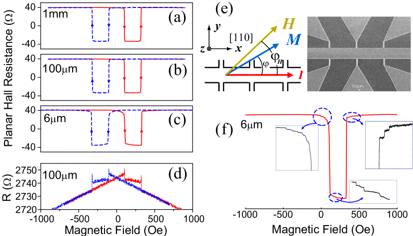
Magnetoresistance measurements are carried out on families of Hall bars (widths 6 m–1 mm), and square van der Pauw devices (33 mm2). The former are aligned along the [110] direction by a combination of photo- and electron-beam- lithography. Voltage probes on the Hall bars are carefully designed to minimize their perturbation upon current flow within the devices (cf. SEM micrograph, Fig. 1e). Standard four-probe lock-in measurements are performed by a 10 nA ac sensing current at 14 Hz, excitation is intentionally kept quite low to obviate electron heating. Magnetic fields are generated using a 3-coil superconducting magnet that allows 3D field orientation without physically disturbing the sample. We execute two classes of experiments, the first in which the field orientation is fixed in-plane along a specific direction, , with respect to the longitudinal axis of the Hall bars, while the field magnitude is swept linearly between 1000 Oe. In the second, we fix the magnitude of the applied in-plane field, while stepping its orientation clockwise or counter-clockwise. Prior to each sweep, an in-plane field of 6000 Oe is applied to saturate the sample magnetization, .
At all angles, except for those along (110) directions, two abrupt jumps are observed in PHE measurements. Families of data taken from Hall bars spanning from 6 m to macroscopic (1 mm) dimensions are shown in Fig. 1(a-c). These are obtained for orientation 20∘ away from [110]. For comparison, the field-dependent sheet resistance of a 100 m Hall bar is also displayed in Fig. 1d.
Four distinct features emerge. a) Large switching events at distinct magnetic fields are observed in the Hall resistance; these are accompanied by small jumps (relative to the background) in the longitudinal resistance. b) Between these switching fields, the planar Hall resistance remains constant at approximately 37 . The signal polarity reverses at each switching event. c) The switching fields appear to be independent of sample size and geometry. Measurements on samples with square, van der Pauw geometry, as large as mm2, exhibit identical switching behavior as those of the smaller, micron-scale devices - even though the magnitude of the Hall resistance is reduced in the former, presumably due to non-uniform current distribution. d) When the width of the Hall device is reduced to 6 m, small Barkhausen jumps are observed. These occur in close proximity to the switching transitions (Fig. 1f), and appear to demonstrate that the propagation of domain walls is constrained by geometry. citation8
We have also investigated samples with Hall bars fabricated along many other directions besides the [110] crystalline axis. We find that the switching fields do not depend on the orientation of the Hall bars, whereas the magnitude of planar Hall resistance jumps are systematically reduced as one moves away from the (110) directions.
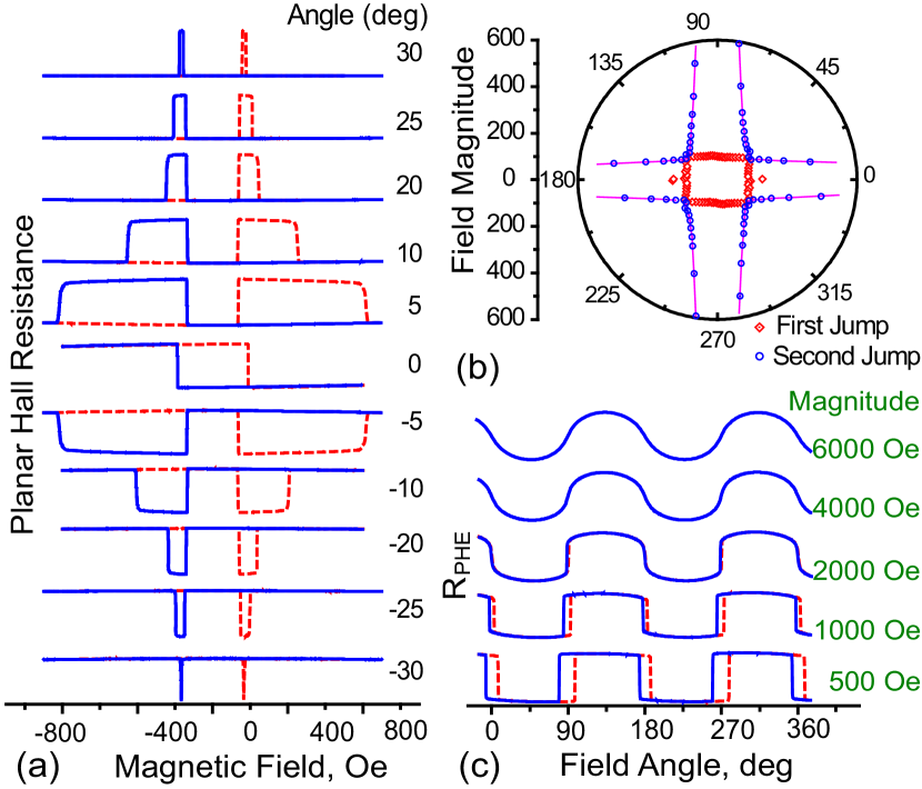
Figure 2a presents the dependence of – loops upon field orientation angle as it is varied from to 30∘ in the plane. In the field range of these experiments, only one jump occurs along the (110) directions. Away from these special orientations, a two-jump reversal is always observed. The first switching field is almost constant, while the second switching field decreases dramatically and approaches at around 30∘.
We interpret the jumps in the Hall resistance as follows. The electric field within a single domain ferromagnetic film with in-plane magnetization can be written as citation5
| (1) | |||||
| (2) |
where the current density is assumed to be uniformly distributed along the Hall bar, and are the longitudinal and transverse axes, and is the angle between the magnetization and current density . and are the resistivities for current oriented parallel and perpendicular to the magnetization. The anisotropic magnetoresistance phenomenon is described by Eq. 1. The transverse resistance, i.e. the planar Hall resistance, is expressed in Eq. 2; it exhibits extrema at = 45∘ and its cubic equivalents. To verify this angular dependence of the planar Hall resistance, an in-plane field of constant magnitude 6000 Oe is applied to saturate the magnetization, and its orientation is swept through 360 degrees (Fig. 2c). In accordance with Eq. 2, the measured Hall resistance exhibits extrema for applied field orientations of 45∘, 135∘, 225∘, and 315∘. Note that the first maximum of planar Hall resistance appears at 135∘ instead of 45∘, indicating ( from Eq. 2). This property of (Ga,Mn)As is distinct from that in conventional ferromagnetic metals, where . It may originate from the different manner in which holes and electrons contribute to the spin-orbit interaction in ferromagnetic materials.
The anomalous switching behavior of the Hall resistance shown in Figs. 1(a-c) can be explained by a two-jump sequence of magnetization: [100] ( -45∘) [010] ( 45∘) [00] ( 135∘). This evolution also accounts for the accompanying small longitudinal resistance jumps shown in Fig. 1d. Between the switching events, the sample remains in what appears to be a macroscopic single domain state. In this regime the magnetization evidently rotates coherently according to Stoner-Wohlfarth model, citation9 hence the planar Hall resistance continues to evolve to a small degree with field. Scanning SQUID microscopy of (Ga,Mn)As epilayers magnetized in-plane have provided evidence for the existence of macroscopic single domains on length scales extending to hundreds of microns. citation11 Domain states within the sample exist only in the vicinity of the switching field, and the associated domain wall scattering evidently generates the remarkable resistance spikes shown in Fig. 1d.
Figure 2b summarizes the signatures of the coercive fields manifested in our electrical transport measurements. The field loci delineating the resistance transitions are shown in polar coordinates. The lines form a rectangular shape, whereas the lines are more complicated. The latter follow the extrapolation of lines at low field but evolve towards the (110) axes in higher fields. Eventually, at a field around 2500 Oe, the second jump becomes smeared and reversible. These measurements clearly elucidate behavior that is generic in our (Ga,Mn)As epilayers: the in-plane magnetic anisotropy is nearly cubic, but it is biased by a small two-fold preference along [110].
Unusual multiple switching, somewhat analogous to that demonstrated in this work, has also been observed in ultrathin epitaxial Fe films, through the magneto-optic Kerr effect (MOKE). A switching pattern analogous to that of Fig. 2b was measured in Ag/Fe/Ag(001) system by Cowburn et al., citation12 although with significantly less resolution in their metallic system. To explain their results a simple model is invoked, incorporating a well-defined domain wall pinning energy into a complex, anisotropic magnetocrystalline energy surface (A weak in-plane uniaxial anisotropy is superimposed along one easy axis of a strong cubic anisotropy). Our experimental data can be explained via similar domain reversal energetics, but in the present case the in-plane uniaxial easy axis is collinear with a hard axis of the cubic anisotropy. The corresponding free energy density of such a single domain magnet can be written as, . Here , are in-plane uniaxial and cubic anisotropy constants. The equilibrium state is defined by the conditions, and . The former gives,
| (3) |
At zero field, four distinct magnetization states, corresponding to four local energy minima, can exist: ,, with . Domains can exist over short length scales in a demagnetized thin film. Upon application of an in-plane field, these small-scale domains quickly become suppressed and the whole sample evolves into a macroscopic single domain state with close to one of the zero fields minima . When the external field is reversed, magnetization reversal is achieved via an intermediate state corresponding to the sample magnetization oriented almost orthogonally (90∘) to the initial and final directions of the magnetization. Domain states mediate the transitions from one energy minimum to another. For a domain wall to become liberated to propagate through the sample, the reversed external field must be increased to the point where a characteristic pinning energy density, , is exceeded, i.e., . Here are the initial and final magnetization, and is the switching field. If is small compared to the cubic anisotropy field, coherent rotation of and from the zero-field equilibrium is negligible. For transitions from [100] to [010], a 90∘ domain wall with core magnetization along [110] is required to propagate across the sample, giving , in which is the corresponding domain wall pinning energy density. Considering all possible orientational trajectories, we can describe the loci of transitions as and . At low field, these describe two parallel sets of lines that are in excellent correspondence with the switching pattern observed in our experiments (Fig. 2b). At high fields two new pieces of physics become important. First, coherent rotation of M must be considered and, second, the energy density of a domain wall also becomes significantly reduced. citation13 As a result, high field transitions progressively evolve towards the (110) directions.
Several additional points are worthy of mention. First, PHE measurements enable determination of crystallographic orientation with remarkable precision; we estimate that the angular error in establishing the (110) crystalline axes is less than 0.04∘. Second, apart from the singularity along these (110) directions, neither single transitions nor three-transition processes are observed. This justifies our assumption that in-plane uniaxial anisotropy does not exist along the cubic easy axes. citation14
We are able to deduce both the cubic and uniaxial anisotropy fields through PHE measurements. To achieve this, a large, constant magnetic field is applied in the plane while its orientation is rotated continuously. Fig. 2c shows data from such measurements for clockwise and counterclockwise sweeps of magnetic field orientation, for a family of field magnitudes. When , where 2500 Oe is the dominant cubic anisotropy field, the magnetoresistance reverses each time the magnetization switches across the cubic hard axis. The planar Hall resistance becomes reversible for fields greater than 2500 Oe, in which case the magnetization rotates coherently according to Stoner-Wohlfarth model. Thus, for a given external field angle , the macroscopic in-plane magnetization orientation, , can be calculated by using expression in Eq. 2. Fitting all the computed data sets () to Eq. 3, we consistently and unambiguously extract the anisotropy fields Oe, Oe.
Progress has recently been made toward gaining a theoretical understanding of magnetic anisotropy in III-V magnetic semiconductors. citation15 ; citation16 It is generally agreed that, in addition to an intrinsic cubic anisotropy, (Ga,Mn)As possesses a substantial out-of-plane uniaxial component with sign that is dependent on whether tensile or compressive biaxial strain exists at the interface. citation7 While attention has focused almost exclusively on the out-of-plane magnetic anisotropy, recent work on (Ga,Mn)As magnetic tunnel junctions TanakaHigo highlights the importance of the in-plane anisotropy. On the other hand, theoretical models of cubic anisotropy predict that the in-plane cubic easy axes can be oriented along either (100) or (110) depending upon the hole concentration and the degree of spin-splitting. By contrast, all of our data to date, on a variety of (Ga,Mn)As epilayers, indicate that the cubic easy axes are aligned along (100) axes. Further PHE studies on additional epilayers are needed to determine if the cubic anisotropy exhibits the variations predicted by theory. Our experimental results do agree, however, with predicted magnitude of the cubic anisotropy field, which we find to be about 2400 Oe.
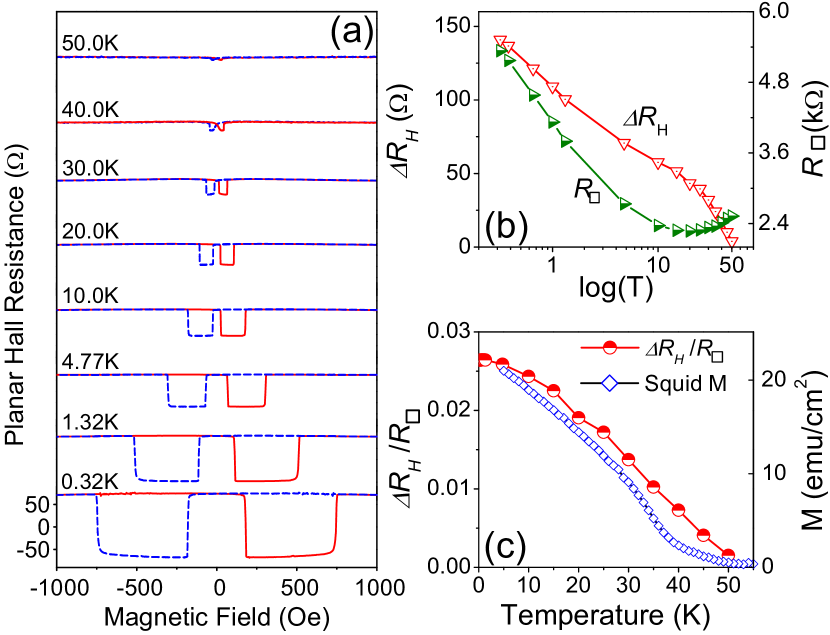
We have also studied the temperature dependence of PHE, which should be of significant importance in elucidating its underlying physical mechanisms. Fig. 3a shows the results for a 10 m Hall bar, measured under conditions of careful temperature regulation, stepped downward from 50K to 0.32K, for fixed-orientation, swept-magnitude, applied magnetic fields. The magnitude of both PHE and the coercive fields increases rapidly with decreasing temperature (Fig. 3b). For K, both the PHE and sheet resistivity appear to diverge logarithmically down to the lowest measured temperatures, while the ratio remains nearly constant. Here, is the PHE resistance jump and is the zero-field sheet resistance. This ratio, , should provide valuable information about the hole spin polarization. We find that it decreases monotonically with increasing temperature, qualitatively tracking the magnetization of a 33 mm2 sample measured by SQUID magnetometry(Fig. 3c).
In conclusion, these first observations of a giant planar Hall effect in (Ga,Mn)As devices enable systematic investigation of in-plane magnetic anisotropy and magnetization reversal via electrical transport measurements. In semiconducting materials, GPHE measurements provide unique advantages over magneto-optical techniques. For example, carrier concentration changes arising from sample illumination can be circumvented. It is also notable that the high signal-to-noise attainable in GPHE measurements permits observation of behavior that emerges only in structures of reduced dimensions (e.g. Barkhausen jumps in 6 m devices). Given the minimal excitation power required, this technique is compatible with very low temperature measurements (mK), thus offering new possibilities for investigations in micro- and nanoscale spintronic devices.
We gratefully acknowledge support from DARPA under grants DSO/SPINS -MDA 972-01-1-0024 (Caltech) and DARPA/ONR N00014-99-1-1096 (UCSB), and from the AFOSR under grant F49620-02-10036 (UCSB). We also thank Prof. P.E. Wigen for valuable discussions.
References
- (1) G. Prinz, Science 282, 1660 (1998).
- (2) S. A. Wolf et al., Science 294, 1488 (2001).
- (3) H. Ohno et al., Nature 401, 944 (2000).
- (4) G. Schmidt et al., Physica E 10, 84 (2001).
- (5) J. P. Pan, Solid State Physics, F. Seitz and D. Turnbull, Eds., New York Academic Press, 1957, V. 5, p. 1-96.
- (6) K. Hong and N. Giordano, Phys. Rev. B51, 9855 (1995).
- (7) H. Ohno et al., Science 281, 951 (1998).
- (8) J. Wunderlich et al., IEEE Trans. Magn. 37, 2104 (2001). T. Ono et al., Science 284, 468 (1999).
- (9) E. C. Stoner and E. P. Wohlfarth, Philos. Trans. R. Soc. London A 240, 74 (1948).
- (10) T. Fukumura et al., Physical E 10, 135 (2001).
- (11) R. P. Cowburn et al., J. Appl. Phys. 78, 7210 (1995).
- (12) Magnetic domains, A. Hubert and R. Sch fer, Springer-Verlag, Berlin, 1998, p. 235.
- (13) R. P. Cowburn, S. J. Gray, and J. A. C. Bland, Phys. Rev. Lett. 79, 4018 (1997).
- (14) T. Dietl, H. Ohno, and F. Matsukura, Phys. Rev. B 63, 195205 (2001); T. Dietl et al., Science 287, 1019 (2000).
- (15) M. Abolfath et al., Phys. Rev. B 63, 054418 (2001); J. König, T. Jungwirth, and A. H. MacDonald, Phys. Rev. B 64, 184423 (2001).
- (16) M. Tanaka and Y. Higo, Phys. Rev. Lett. 87, 026602 (2001).