Steps on current-voltage characteristics… \sodtitleSteps on current-voltage characteristics of a silicon quantum dot covered by natural oxide \rauthorS. V. Vyshenski, U. Zeitler, and R. J. Haug \sodauthorVyshenski, Zeitler, Haug \dates2 October 2002*
Steps on current-voltage characteristics of a silicon quantum dot covered by natural oxide
Abstract
Considering a double-barrier structure formed by a silicon quantum dot covered by natural oxide with two metallic terminals, we derive simple conditions for a step-like voltage-current curve. Due to standard chemical properties, doping phosphorus atoms located in a certain domain of the dot form geometrically parallel current channels. The height of the current step typically equals to pA, where is the number of doping atoms inside the domain, and only negligibly depends on the actual position of the dopants. The found conditions are feasible in experimentally available structures.
73.23.Ps, 73.23.Hk
The fabrication of nanostructures became possible through recently developed new technologies [1, 2]. Individual silicon quantum dots (SQD) reported in [2] are spherical particles with diameters in the range 5\ch12 nm covered by a 1\ch2 nm-thick natural film. Metallic current terminals made from degenerately doped are defined lithographically to touch each individual dot from above and from below.
To ensure metallic electrodes the donor concentration should be , where cm-3. The critical concentration is defined by the Mott criterion [4], introducing the transition to a metallic type of conductivity in a semiconductor at:
| (1) |
where is the Bohr radius of an electron bound to a donor inside the crystal, in the case of phosphorus-donors nm [4].
As for the doping of the dot, the situation concerning a Mott transition in that small dots is much less trivial than the one described by Eq. (1). Let us consider dots with diameters nm formed from n-doped with as an illustrative example. Then each dot contains in average one donor. Note that we will consider degenerately -doped electrodes with which ensures metallic conduction up to the borders of the dot.
Real fabrication technology [2] provides a wafer with hundreds of SQDs on it with current leads towards each individual SQD. Dots in average have the same value of mean dopant concentration , which is determined by the parent material of bulk silicon the dots are formed from. However, on the level of each individual SQD we will always have exactly integer number of doping atoms. If, as in the example above, the average number of dopants the actual number of donors in the dot can have values , with values larger than these very unlikely.
Our objective is to illustrate, that SQDs from the same wafer fall into several distinct sets of approximately the same conductance. The typical value of conductance for each set is nearly completely determined by the number of donors present in a certain part of a SQD so that labels each set of SQDs.
Summarizing the above, we need for a quantization of the conduction through a dot with donors the following conditions:
-
•
Size of the dot comparable with Bohr radius: .
-
•
Average doping of the dot , leading to a mean number of dopants , so that are the most probable configurations of an individual SQD.
-
•
Doping of the electrodes , so that current leads are perfectly metallic.
-
•
Dot covered by an oxide layer thick enough to suppress ballistic transport through the dot.
In fact all these condition can be simultaneously satisfied for SQD fabricated with the method mentioned above [2].
Model system. We use a simple model of a cubic SQD with (we will use nm for estimates), covered with an oxide layer with thickness nm, height [3] eV and contacted with current terminals from left and from right. The -axis is oriented from left to right along the current flow, as shown in Fig.1.
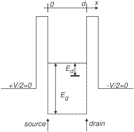
A tunneling current is injected into the dot via the oxide barrier from the top (source at ) and leaves the dot at the bottom (drain at ). Due to the presence of the oxide barriers this current is non-ballistic and non-thermal. We assume that the high potential barriers associated with the oxide layers are not much affected by the voltage and the tunneling charges. We concentrate on what happens between these effective source and drain (Fig.2), as in [5].
In the case when the dot can be regarded as an insulating system it is reasonable to assume that the applied voltage equally drops over the potential barriers and the dots. For simplicity we neglect the difference of the dielectric constants of the oxide barriers and the dot. In this approximation we can introduce an effective voltage describing the part of the total transport voltage applied between effective source and drain which drops across the dot itself.
In this rude approximation we neglect the effect of spatial quantization upon values on the ionization energy, the conductivity gap and material parameters of silicon.
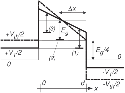
Dot without donors. At the Fermi level inside the dot is situated in the middle of the gap, i.e. bellow the conduction band edge ( eV at 300 K).
As grows, the bottom of the (still empty) conduction band bends down accordingly. When the conduction band in the dot close to the drain aligns with the Fermi level of the emitter we expect a drastic increase in the tunneling current. This threshold voltage (Fig.2) for is given by , regardless of the number of dopants in the dot (as long as the dot is not yet metallic, of course). In the following we therefore limit our studies to voltages
| (2) |
In this voltage range we have a -thick barrier (formed by the dot) with always finite height between effective source and drain. The intrinsic concentration of electrons and holes at 300 K is cm-3. Even at this high temperature the probability to have at least one intrinsic electron in a dot with size nm is only . So we would expect virtually no current in this mode. This is confirmed by direct electrical tests [2] of SQD with the required properties.
Single-donor channel. Let us now consider one single donor in the dot located at with ionization energy [3] eV (for P as a donor).
At zero temperature current is due to resonant tunneling via non-ionized donor (as in [6] for example). Differential conductance for the states with energy is
| (3) |
where is linewidth of state of electron bound to the donor due to coherent mixing with conduction states to the left (right) of the left (right) tunnel barrier.
Oxide barriers (with height eV and width nm) give dominant contribution to compared to contribution of the body of the dot (with typical height eV and width nm). So, we can approximate with linewidth for the case of an impurity localized at distance inside rectangular one-dimensional tunnel burrier [6] of height :
| (4) |
where is (true, not effective) electron mass, , and is Fermi wave number in the contact electrodes. The numerical estimate in (4) is given for the electrodes doped up to as in [2].
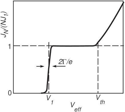
From Fig.2 it is clear that resonant energy . This means that as soon as effective Fermi level reaches a certain threshold , tunnel current flowing through the structure acquires a step-like increase of
| (5) |
If the impurity is located near the drain, i.e. (as donor 1 in Fig.2), then threshold for the effective voltage is given by
| (6) |
In contrast, for an impurity located at distances from the drain (i.e. further away than the threshold case of donor 2 in Fig.2), no additional current channel via a single impurity can be opened at low enough voltages defined in (2) where virtually no background current is present. In the present case this value nm, which returns us to the above criterion: only impurities located in the immediate vicinity (defined within the accuracy ) of the drain contribute to the single-impurity channel.
This shows that in first approximation the conductance of this channel does not depend on . As shown above, a single-impurity channel already only selects impurities located within a very narrow range of close to the drain.
Two-, three-, multi-donor channel. The above consideration shows, that due to the bend of the bottom of conduction band following the transport voltage, there is no chance to notice current flowing through a sequential chain of impurities (such as donors 1 and 3 in Fig.2), connecting source and drain. The contribution of such a chain will be totally masked by the current flowing directly via the conduction band. The only way for multiple impurities to manifest themselves in quantized conductance is to form multiple geometrically parallel singe-impurity channels situated close enough to the drain as considered above.
Therefore, if impurities fall into the thin layer near the drain to approximately the same coordinate as that of donor 1 in Fig.2 (within the Bohr radius), we will see a switching-on of an -fold channel with current
| (7) |
at the same threshold voltage V as for a single-donor channel (Fig.3).
All the above considerations are only valid as long as the dot itself can be regarded as an insulating system. As the number of donors in a SQD grows, the dot becomes a metallic particle, and the conduction band edge in the dot aligns with the Fermi level of the electrodes. In a very simple estimate we define this transition to a metal when the total volume of donors with an individual volume of exceeds the volume of the dot. This is an exaggerated version of the Mott criterion (1) which holds not only in bulk, but in a small structure, too. For the analyzed example from above this gives as a limiting value. The practically interesting set for both and considered above is still far bellow this limit.
Quite a number of other mechanisms of electron transport might take place in this system. Surprisingly, even taking into account such other mechanisms [7] does not change much the main idea of the present paper.
In small dots with diameter nm the domain with active dopants extends to the whole dot, and thus . In large dots with diameter nm the domain with active dopants is less than the dot itself and is localized near the drain. Hence the position of the domain, number and value all can be different for the current flowing in different directions. Really, when sign of applied voltage changes, the source and the drain change places.
In a certain sense the discrete increase of dot’s conductivity which follow the increase of the dopants number could be regarded as a mesoscopic analog of the Mott transition between insulating and conducting states of the system.
Useful discussions with I. Devyatov, M. Kupriyanov, and S. Oda are gratefully acknowledged.
References
- [1] L. J. Guo, E. Leobandung, L. Zhuang et al., J. Vac. Sci. Technol. B 15, 2840 (1997).
- [2] A. Dutta, M. Kimura, Y. Honda et al., Jpn. J. Appl. Phys. 35, 4038 (1997). S. Oda, K. Nishiguchi, Journal de Physique IV, 11 (Pr.3), 1065 (2001).
- [3] O. Madelung (ed), Physics of Group IV Elements and III-V Compounds (Springer-Verlag, Berlin, 1982), Subvolume III/17a of Landolt-Börnstein New Series.
- [4] N. F. Mott, Metall-Insulator Transitions (Taylor & Francis, London, 1990, 2-nd edition), Chap. 5.
- [5] J. Schwinger, Particles, sources, and fields (Addison-Wesley, Reading, 1970).
- [6] A. I. Larkin and K. A. Matveev, Zh. Exp. Theor. Phys. 93, 1030 (1987).
- [7] I. A. Devyatov and M. Yu. Kupriyanov, JETP 77, 874 (1993).