J. Carlos Eguesa)Guido Burkard
Daniel Loss
Department of Physics and Astronomy, University of
Basel, Klingelbergstrasse 82, CH-4056 Basel, Switzerland
Abstract
We consider a two-channel spin transistor with weak spin-orbit induced
interband coupling. We show that the coherent transfer of carriers between
the coupled channels gives rise to an additional spin rotation. We
calculate the corresponding spin-resolved current in a Datta-Das geometry
and show that a weak interband mixing leads to enhanced spin control.
pacs:
71.70.Ej,72.25.-b,73.23.-b,73.63.Nm
a)Also at: Department of Physics and
Informatics, University of São Paulo at São Carlos, 13560-970
São Carlos/SP, Brazil; electronic mail: egues@if.sc.usp.br
The pioneering spin-transistor proposal of Datta and Das datta best
exemplifies the relevance of electrical control of magnetic degrees of
freedom as a means of spin modulating charge flow. In this device exp, a spin-polarized current spin-pol; egues injected from the source is
spin modulated on its way to the drain via the Rashba spin-orbit rashba (s-o) interaction, Fig. 1(a). The spin transistor operation relies
on gate controlling nitta the strength of the Rashba
interaction which has the form in a strictly 1D channel rashba. Upon crossing the Rashba-active
region of length , a spin-up incoming electron emerges in the
spin-rotated state
(1)
where is
the rotation angle and is the electron effective mass
datta. The corresponding spin-resolved conductance is found
to be .
Here we extend the above picture by considering a geometry with two
weakly-coupled Rashba bands in the quasi-one-dimensional channel, Fig. 1(b).
We treat the degenerate states near the band crossings perturbatively in
analogy to the nearly-free electron model am. This approach allows
for a simple analytical description of the problem. We calculate the
spin-resolved current by extending the usual procedure of Datta and Das datta to account for weakly coupled bands. Our main finding is an additional spin rotation for injected electrons with energies near the band
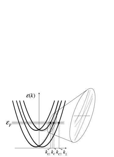
crossing [see shaded region around in Fig. 2]. As we
derive later on, an incoming spin up electron in channel a emerges
from the Rashba region in the rotated state
(2)
where is the additional spin rotation
angle, the interband matrix element and the wave vector at the
band crossing, Fig. 2. From (2) we can find the new spin-resolved
conductance
Model. We consider a quasi-one-dimensional wire of length with
two bands a and bdescribed by and
eigenfunctions where the ’s denote the transverse confinement wave functions. In the presence of the
Rashba s-o interaction, we can derive a Hamiltonian for the system in the
basis of the uncoupled wave functions .
This reads,
(4)
where , , , (, ) and we have considered to be the eigenbasis of . For the
Hamiltonian in (4) is diagonal and yields uncoupled Rashba
dispersions (thin lines in Fig. 2); the
corresponding wave functions are (here ). Note that for the bands
cross for some values of . For instance, for a crossing occurs at For non-zero
interband coupling moroz, we can diagonalize
exactly (see Mireles and Kirczenow in Ref. moroz) to
find the new dispersions (thick lines in Fig. 2).
Bands near . Since we are interested in transport with
injection energies near the crossing, we follow below a simpler perturbative
approach am to determine the energy dispersions and wave functions
near . Near the crossing we can solve the reduced Hamiltonian
(5)
which to lowest order yields
(6)
As shown in the inset of Fig. 2, Eq. (6) describes very well the
anti-crossing of the bands near . The corresponding zero-order
eigenstates are
(7)
where the sub-indices indicate the respective channel. The analytical form
in (6) allows us to determine the wave vectors and
in Fig. 2 straightforwardly: we assume and and solve (assumed ) to find
(8)
Note that to the lowest order used here the horizontal splitting
is constant and symmetric about .
Boundary conditions. We now consider a spin-up electron entering the
Rashba-active region of length in the wire. Following the usual
approach, we expand this incoming state in terms of the coupled Rashba
states in the wire. We consider only the states , , and in the expansion
(9)
The above ansatz satisfies the boundary conditions for both the wave
function and (to leading order) its derivative . More explicitly, the
velocity operator condition molenkamp at for an electron with yields
(10)
where we used (still valid to leading order). The ‘four-vector’ notation in (10) concisely specifies the spin states in
channels a (upper half) and b (lower half). Note that Eq. (10) is satisfied provided that . This inequality is
satisfied in our system for realistic parameters.
Underlying the ansatz in (9) is the assumption of unity
transmission through the Rashba region. Here we have in mind the particular
spin-transistor geometry sketched in Fig. 1(a): a gate-controlled
Rashba-active region of extension smaller than the total length of the wire. In this configuration, there are only small band offsets
(which we neglect) of the order of at
the entrance and exit of the Rashba region. Hence
transmission is indeed very close to unity, see Ref. [egd, ]. The
boundary conditions at are also satisfied.
Generalized spin-rotated state. From Eq. (9) we find that a
spin-up electron entering the Rashba region at emerges from it at
in the spin-rotated state
(23)
(28)
which is essentially Eq. (2). Observe that in absence of interband
coupling (i.e., ) Eq. (28) reduces to the Datta-Das
state in (1). An expression similar to (28) holds for the
case of an incoming spin-down electron.
Spin-resolved current. For we have
(34)
which describes planes waves in the uncoupled channels a and
b arising for an incoming spin-up electron in channel a. The
total current follows straightforwardly (Landauer-Büttiker) from Eq. (34)
(35)
where is the applied bias between the
source and drain. The spin-dependent conductance in (3)
follows immediately from (35). Equation (35)
clearly shows the additional modulation of the
spin-resolved current due to s-o
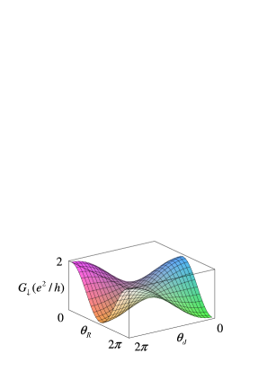
induced interband coupling. Figure 3 illustrates the angular dependence of as a function of and . The s-o
mixing angle enhances the possibilities for spin control in
the Datta-Das transistor.
Realistic parameters. For concreteness, let us consider infinite
transverse confinement (width ). In this case, and the interband coupling constant . We choose , which
implies (i) eVm
(and meV) for and nm, (ii) [ should be tuned to ], and (iii) .
Assuming nm [Rashba region length, Fig. 1(a)], we find and , since . This is a conservative estimate. In principle, can be
varied independently of via lateral gates which alter .
Note also that [validity of Eq. (10)] for the above parameters. Finally, we note that the most
relevant spin-flip mechanism (Dyakonov-Perel) should be suppressed
in quasi-one-dimensional systems such as ours bournel. In
addition, thermal effects are irrelevant in the experimentally
feasible linear regime datta-book we consider here
This work was supported by NCCR Nanoscience, the Swiss NSF, DARPA, and ARO.
We acknowledge useful discussions with D. Saraga.
List of references
References
(1) S. Datta and B. Das, Appl. Phys. Lett. 56, 665
(1990).
(2) G. Meir, T. Matsuyama, and U. Merkt, Phys. Rev. B 65, 125327
(2002); C.-M. Hu, J. Nitta, A. Jensen, J. B. Hansen, H.
Takayanagi, T. Matsuyama, D. Heitmann, and U. Merkt, J. Appl. Phys. 91, 7251 (2002).
(3) R. Fiederling, M. Keim, G. Reuscher, W. Ossau,
G. Schmidt, A. Waag, L. W. Molenkamp, Nature 402, 787
(1999); Y. Ohno, D. K. Young, B. Beschoten, F. Matsukura, H. Ohno,
D. D. Awschalom, Nature 402, 790 (1999).
(4) J. C. Egues, Phys. Rev. Lett. 80, 4578 (1998).
(5) Yu. A. Bychkov and E. I. Rashba, JETP Lett. 39,
78 (1984).
(6) J. Nitta T. Akazaki, H. Takayanagi, and T. Enoki,
Phys. Rev. Lett. 78, 1335 (1997); G. Engels, J. Lange,
Th. Schäpers, and H. Lüth, Phys. Rev. B 55, R1958
(1997); D. Grundler, Phys. Rev. Lett. 84, 6074 (2000);
Y. sato, T. Kita, S. Gozu, and S. Yamada, J. Appl. Phys.
89, 8017 (2001).
(7) N. W. Ashcroft and N. D. Mermin, Solid State Physics,
Ch. 9. (Holt, Rinehart, and Winston, New York, 1976).
(8) A. V. Moroz and C. H. W. Barnes, Phys. Rev. B 60,
14272 (1999); F. Mireles and G. Kirczenow, Phys. Rev. B
64, 024426 (2001); M. Governale and U. Zülicke, Phys.
Rev. B 66, 073311 (2002).
(9) J. C. Egues, G. Burkard, and D. Loss,
Phys. Rev. Lett. 89, 176401 (2002)).
(10) E. A. de Andrada e Silva, G. C. La Rocca, and F. Bassani, Phys. Rev. B
55, 16293 (1997); L. W. Molenkamp, G. Schmidt, and G.E.W.
Bauer, Phys. Rev. B 64, R121202 (2001).
(11) A. Bournel, P. Dollfus, P. Bruno, and P. Hesto, Eur. Phys. J. AP 4,
1 (1998).
(12) S. Datta, Electronic transport in mesoscopic
systems (Cambridge University Press, Cambridge, 1997), Ch. 2, p.
89.
Figures
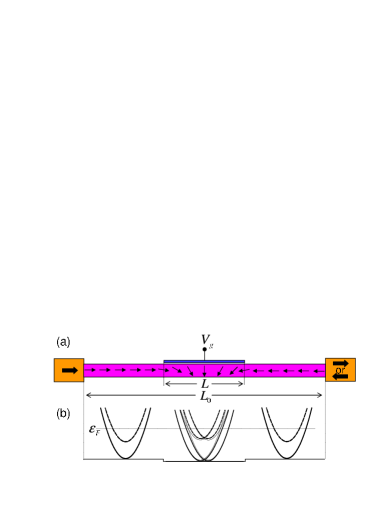
Figure 1: Spin transistor geometry with a two-band channel. (a) The length
of the Rashba region is smaller than the total length of the wire. (b)
Sketch of energy dispersions in the s-o active region with and without
interband coupling (Rashba bands) and away from it (parabolic bands). Note
the small band offsets between adjacent regions in the wire.Figure 2: Band structure in the presence of spin-orbit coupling. In absence
of interband mixing the Rashba dispersions are uncoupled (thin solid lines)
and cross at, e.g., . For non-zero interband coupling the bands anti
cross (thick solid lines). The inset shows a blowup of the dispersion region
near the crossing: the approximate solution [dotted lines, perturbative
approach, Eq. (6)] describes well the energy dispersions
near . Figure 3: Angular dependence of the spin-down conductance. The additional
modulation due to s-o interband mixing and can be varied independently.