Spin Injection: Interface Resistance in Fe/Semiconductor Junctions Calculated from First Principles
Olaf Wunnicke111Institut für Festkörperforschung, Forschungszentrum Jülich, D-52425 Jülich, Germany, Phivos Mavropoulos1, and Peter H. Dederichs1
Abstract
We calculate the current spin polarisation and the interface resistance of Fe/GaAs and Fe/ZnSe (001) spin injection junctions from first principles, including also the possibility of a Schottky barrier. From our results of interface resistance we estimate the barrier thickness needed for efficient spin injection if the process is non-ballistic.
Key words:
spin injection; spin dependent transport; interface resistance
Running title:
Spin Injection in Fe/Semiconductor Junctions
Corresponding author:
Olaf Wunnicke, Institut für Festkörperforschung,
Forschungszentrum Jülich, D-52425 Jülich, Germany
email: o.wunnicke@fz-juelich.de
tel.: +49-2461-61-4799, fax: +49-2461-61-2620
The achievement of spin-polarised electric transport via the conduction band of semiconductors (SC) is one of the central issues in the field of spintronics. Potential technological applications have already been proposed since 1990 [1], but the conditions under which this can be realised are not yet clear, neither experimentally nor theoretically. The bottleneck seems to be the injection of the spin-polarised current from a ferromagnetic metal (FM) contact into the SC. One basic reason for this was revealed by Schmidt and collaborators [2], who argued that the huge conductivity mismatch of the FM and the SC, in correlation with the much smaller spin-flip mean free path in the FM, will lead to a drastic drop of the spin polarisation of the current in the vicinity of the interface. There are, in theory, two ways to circumvent the obstacle: the ballistic spin injection and the injection through a spin-selective tunneling barrier. At least the latter has already been used in praxis with considerable success [3].
The possibility of ballistic spin injection was proposed by Grundler [4]. First-principles calculations [5, 6, 7] have shown the necessity to consider the full band structure of the FM and SC together with the electronic structure of the interface. Then the difference in symmetry of the FM and SC for the minority-spin wave functions can play the most important role, by essentially disallowing the incoming FM minority electron to pass onto a SC state. Spin polarisations and magnetoresistance ratios of up to the ideal 100% were calculated for Fe/GaAs(001), Fe/ZnSe(001), and Fe/InAs(001) systems.
In parallel to this, there is also the proposal of Rashba [8] and Fert and Jaffrès [9] that a tunneling barrier at the FM/SC interface could solve the problem even in the diffusive regime. The idea is that a tunneling barrier can be highly spin selective, as shown in TMR junctions, and at the same time provides an extremely high interface resistance; this combination of properties would lead to spin injection even in the troubling diffusive regime.
In this contribution we extend our previous work [5] to the evaluation of interface resistance for majority and minority electrons in Fe/GaAs and Fe/ZnSe (001) junctions, with or without a tunneling barrier, in the approach developed in Ref. [10], and compare to the limits set by the Fert-Jaffrès theory. Finally, we discuss the importance of interface resonances in such junctions.
Schep and collaborators [10], working in the approximation of the resistor model, have deduced the resistance of a ballistic interface of area between two bulk regions A (in our case Fe) and B (SC) in which conduction channels are randomly mixed due to diffuse scattering, as
| (1) |
Here, is the ballistic transmission probability of the interface. The diffusion is assumed to occur only in the bulk regions. and represent the number of Landauer conduction channels in the two bulk regions, i.e. they are proportional to the area of the projected Fermi surface on the interface plane.
We calculate the electronic structure of the bulk and interface regions in the local density approximation of density-functional theory, using the KKR Green function method, and assuming two independent spin channels. From the Green function the ballistic scattering properties of the interface are obtained using a method equivalent to the Landauer-Büttiker formalism [11]. The scattering at the interface is assumed specular, i.e. the part of the Bloch -vector which is parallel to the interface, , is conserved; the presupposition for this is that the interface is defect-free. The transmission probability can be viewed then as a function of , and is an integral of over the surface Brillouin zone SBZ:
| (2) |
In order to achieve spin injection, the SC conduction band edge must be slightly lower than the Fermi level ; in our calculations we model such a situation by rigidly lowering the SC potential in the region far from the interface. We use a value of as a typical one for an experimental situation. The potential close to the interface, up to two monolayers (ML), is determined by the self-consistent electronic structure and the metal-induced gap states. From this point (3rd ML) on the transition to the bulk-like region would depend on the doping and the exact band offset of the SC, with the possibility of a longer or shorter Schottky barrier. We model the situation by either a gradual lowering of the potential up to the final bulk value, thus describing a Schottky tunneling barrier, or by an abrupt lowering of the potential to the final bulk value; more details are given in Ref. [5]. The former situation is relevant for the case of spin injection through a tunneling barrier with an extremely high interface resistance and spin selectivity. As explained in Refs. [5, 6], for the evaluation of the current spin polarisation the calculation of at is enough for tunneling or thermal spin injection; for the interface resistance the integration of eq. (2) must be employed, but we note that it can be limited within a small circle around , because of the tiny Fermi sphere in the SC.
In the semiconductor part, the low value of means that the corresponding Fermi sphere is extremely small; then the conducting channels of the SC are much fewer than the ones in Fe, and in eq. (1) . Next, one should compare with . In the case of a tunneling barrier, is expected to be so small that will be negligible and the interface resistance will be dominated by the ballistic specular scattering. This remains true even in the absence of a tunneling barrier, because is of the order of for majority spin electrons (and orders of magnitude less for minority) [5], making of the order of or less.
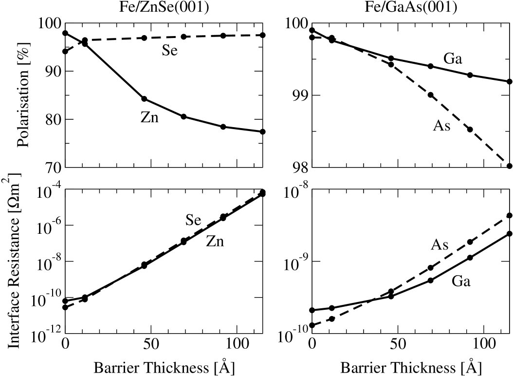
The results obtained for Fe/ZnSe and Fe/GaAs are presented in Fig. 1. In the upper plots the current spin polarisation is shown, as a function of barrier thickness, for all possible terminations of the SC part. The high degree of polarisation is due to the symmetry mismatch of the incoming minority Fe states, as explained in Ref. [5]. The values obtained for the polarisation by use of eq. (2) are somewhat smaller than at , because at nonzero the symmetry mismatch for minority is not strict.
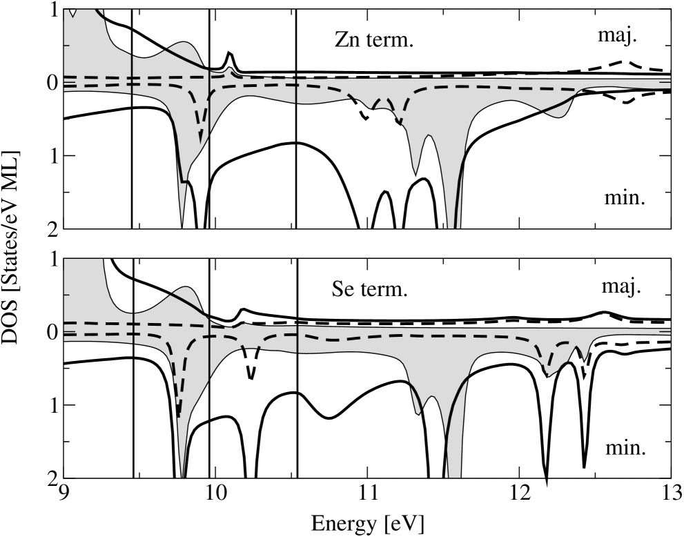
In all cases except the Se terminated Fe/ZnSe system, the current spin polarisation decreases for thicker Schottky barriers; this shows mostly in the Zn terminated Fe/ZnSe system. The cause can be traced back to the existence of resonant interface states in the vicinity of the Fermi level for the minority spin. As discussed in Ref. [12], they can contribute to an increase of the tunneling current. The density of states for the Fe/ZnSe interface at is shown in Fig. 2. For the Zn termination, the interface state lies clearly in the vicinity of the Fermi level, while for the Se termination it lies higher and does not contribute to the conductance. However, we must note that effects that are not taken into account here, such as lattice relaxations, a different pinning of the band offset, or a finite bias, could move the resonant states away from or onto the Fermi level. In the latter case the polarisation is strongly affected and can even changes sign, if the peak is at .
In the lower plots of Fig. 1, the interface resistance is presented for various barrier thicknesses. Note the logarithmic scale used for the resistance. For ZnSe the constant slope reflects the exponential decay of the wave functions within the barrier. For GaAs the asymptotic behaviour of an exponential decay presents itself for thicker barriers, because of the smaller band gap of this material.
In order to estimate the range where spin injection with a barrier is most efficient, we take the criterion proposed in Ref. [9]. This reads for the case of spin injection and detection via a second SC/FM interface,
| (3) |
with the SC resistance (normalised to interface area), its thickness (between the barriers) and the spin-flip mean free path. Typically, can be of the order of and of the order of a [9]. According to the results presented in Fig. 1, this places the necessary Schottky barrier thickness in the range of 70Å for ZnSe or 100Å for GaAs, if is of the order of a .
In conclusion, we have performed ab initio calculations of the transmission probability in Fe/ZnSe and Fe/GaAs spin injection devices taking into account the possibility of a Schottky barrier. We have estimated the corresponding interface resistances for several barrier thicknesses and found relevant barrier thicknesses for efficient spin injection, and shown that resonant interface states can lower the spin injection efficiency. Our presentation is relevant for situations where diffusive scattering is present in the bulk.
References
- [1] S. Datta and B. Das, Appl. Phys. Lett. 56, 665 (1990).
- [2] G. Schmidt, D. Ferrand, L. W. Molenkamp, A. T. Filip, and B. J. van Wees, Phys. Rev. B 62, R4790 (2000).
- [3] H. J. Zhu, M. Ramsteiner, H. Kostial, M. Wassermeier, H.-P. Schönherr, and K. H. Ploog, Phys. Rev. Lett. 87, 016601 (2001); A. T. Hanbicki, B. T. Jonker, G. Itskos, G. Kioseoglou, and A. Petrou, Appl. Phys. Lett. 80, 1240 (2002).
- [4] D. Grundler, Phys. Rev. B 63, R161307 (2001).
- [5] O. Wunnicke, Ph. Mavropoulos, R. Zeller, P. H. Dederichs, and D. Grundler, Phys. Rev. B 65, 241306(R) (2002).
- [6] Ph. Mavropoulos, O. Wunnicke, and P. H. Dederichs, Phys. Rev. B 66, 024416 (2002).
- [7] M. Zwierzycki, K. Xia, P. J. Kelly, G. E. W. Bauer, and I. Turek, arXiv:cond-mat/0204422 (unpublished).
- [8] E. I. Rashba, Phys. Rev. B 62, R16267 (2000).
- [9] A. Fert and H. Jaffrès, Phys. Rev. B 64, 184420 (2001).
- [10] K. M. Schep, J. B. A. N. van Hoof, P. J. Kelly, G. E. Bauer, and J. E. Inglesfield, Phys. Rev. B 56, 10805 (1997).
- [11] H. U. Baranger and A. D. Stone, Phys. Rev. B 40, 8169 (1989).
- [12] O. Wunnicke, N. Papanikolaou, R. Zeller, P. H. Dederichs, V. Drchal, and J. Kudrnovský Phys. Rev. B 65, 064425 (2002)
Captions
Fig. 1: Current spin polarization (upper plots) and interface
resistance
(lower plots) of Fe/ZnSe(001) (left panel) and Fe/GaAs(001)
(right panel), as functions of the Schottky barrier thickness.
The solid curves refer to the cases of Zn and Ga termination,
and the dashed to Se and As termination at the interface. The
values are obtained by an integration over the whole SBZ. Note
the different scales in the axes.
Fig. 2: Local DOS of the Fe/ZnSe(001) at with a Zn (upper plot) and a Se (lower plot) terminated interface. The filled gray lines denote the DOS of bulk Fe, the solid lines the DOS for the interface Fe layer, and the dashed lines the DOS of the first ML of ZnSe (Zn ML for the upper plot and Se ML for the lower). The vertical lines indicate the gap region in the ZnSe and in between is the position of the Fermi level. In this plot, the potential is in the ground state position with no Schottky barrier inserted.