[
Current Rectification by Molecules with Asymmetric Tunneling Barriers
Abstract
A simple experimentally accessible realization of current rectification by molecules (molecular films) bridging metal electrodes is described. It is based on the spatial asymmetry of the molecule and requires only one resonant conducting molecular level ( orbital). The rectification, which is due to asymmetric coupling of the level to the electrodes by tunnel barriers, is largely independent of the work function difference between the two electrodes. Results of extensive numerical studies of the family of suggested molecular rectifiers HS-(CH2)m-C6H4-(CH2)n-SH are presented. The highest rectification ratio is achieved at and .
pacs:
PACS numbers: 85.65.+h]
I Introduction
The concept of a molecular rectifier started the field of molecular electronics (moletronics) almost thirty years ago [1]. At present, moletronics is an explosively growing field of experimental and theoretical activity. The molecular rectifier (MR) is still one of the central objects of this research. Even the simplest future application, such as molecular memory, will require high quality MR with sharp voltage thresholds, large current rectification ratios, small time constants, large breakdown voltages and so on. MR demonstrated so far [2, 3, 4] constitute an impressive proof of principle but their electrical parameters are in fact very poor. The situation prompts further investigation of molecular rectification.
Until recently, theoretical analysis of MR had been largely limited to the Aviram and Ratner donor-insulator-acceptor () mechanism [1]. In this design, the highest occupied molecular orbital (HOMO) and the lowest unoccupied molecular orbital (LUMO) are confined to two different parts of the rectifier, and respectively. The insulating bridge prevents the orbitals from “spilling off” to the other part. If such a molecule is placed between two metal electrodes, the current-voltage characteristics of the junction is expected to be highly asymmetric. At a particular voltage applied in the positive direction, the Fermi level of the electrode on side aligns with the LUMO, and the on side aligns with the HOMO. At this voltage, the current rises sharply because the electrons can now be loaded on the LUMO, then tunnel inelastically through the to the HOMO and the escape into the second electrode. In the opposite direction, a similar process does not occur until a much higher applied voltage.
A different mechanism of molecular rectification was described by Ellenbogen and Love [5]. It is based on an energy mismatch between two conducting levels localized on different parts of the molecule. Within the framework, such levels could, for instance, be the LUMOs of and . Under external bias, the levels shift because of the electric field. In the forward direction, the conducting levels align at some voltage, and facilitate resonant transport of electrons between the electrodes. In the reverse direction, the levels move away from each other and the current remains small. Hence molecular rectification.
We note that both described mechanisms require two electroactive molecular levels and a fine balance between potential drops inside the molecule and on the molecule-electrode interfaces. To the best of our knowledge, neither of the mechanism has been realized experimentally.
Recently, an interesting case of molecular rectification was discussed by Krzeminski et al. [6]. They studied theoretically current rectification in Langmuir-Blodgett (LB) films of -hexadecylquinolinium tricyanoquinodimethanide (C16H33Q-3CNQ), which was previously studied experimentally [2, 3]. That molecule was initially considered to be a possible implementation of the Aviram-Ratner mechanism because its active part Q-3CNQ comprised a donor and an acceptor. (The long insulating tail C16H33 was added to help form good LB films.) It was later realized [7] that the Q-3CNQ is, in fact, a molecule and is unlikely to implement the Aviram-Ratner mechanism. The analysis of Ref.[6] confirmed that the bridge does not sufficiently isolate and to keep molecular orbitals localized on either or . Instead, the orbitals were delocalized over the entire Q-3CNQ unit. Krzeminski et al. have attributed the observed rectification to asymmetric position of the LUMO and HOMO with respect to the Fermi levels of the metal and to “asymmetric profile of electrostatic potential across the system”.
The purpose of this paper is to point out that there is, indeed, a simple and general mechanism of molecular rectification where a single electroactive unit is positioned asymmetrically with respect to electrodes and the HOMO and LUMO are positioned asymmetrically with respect to the Fermi level. However, this mechanism does not require such complex molecules as C16H33Q-3CNQ. What is needed is just one conducting molecular level placed closer to one electrode than to the other. Since most of the applied voltage drops on the longer insulating barrier, the conditions for resonant tunneling through the level are achieved at very different voltages for the two opposite polarities. By changing the lengths of the insulating barriers, the rectification ratio can be systematically changed. This mechanism can be realized by relatively simple molecules. For instance, the conductive level could be supplied by a benzene ring. Also, the molecules can be shorter, produced by e.g. self-assembly instead of LB deposition, and therefore more conductive. Indeed, the currents reported in [3] were of order A/molecule, which almost rules out any practical application of such MR. This is obviously a result of having the long aliphatic tail C16H33. There is an experimental evidence that even much shorter alkane chains, like C12, are very resistive and transport there proceeds by hopping processes rather than tunneling [8]. We show below that With simpler conducting and shorter insulating units, MR can achieve rectification ratios in excess of a hundred while remaining fairly conductive.
In the foregoing sections, we discuss the present mechanism of molecular rectification in more detail. We have performed a numerical analysis of the mechanism by calculating the current-voltage (I-V) characteristics of the family of prototype molecular diodes HS-(CH2)m-C6H4-(CH2)n-SH. We have found that rectification ratios of are achievable with such a design.
We mention for completeness that any asymmetric electrode-molecule-electrode junction should in principle produce asymmetric currents at large enough voltages. Such a high-voltage asymmetry due to unequal coupling to the electrodes [9, 10] or to an asymmetric central molecular unit [11] have been observed experimentally and discussed theoretically. However, the current rectification ratios in these studies were of order unity, which is clearly insufficient for practical applications. Zhou et al reported rectification in a molecular monolayer of 4-thioacetylbiphenyl [4]. In that experiment, the two electrodes were different, with different work functions, and different connections to the molecules. The experimental data were interpreted as the standard thermionic emission through an asymmetric barrier.
II A molecular design for current rectification
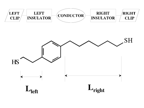
Our molecular rectifiers with asymmetric tunneling barriers consist of five structural parts, see Fig. 1. The end groups provide contact to the two electrodes. For instance, these may be thiols that could self-assemble on the surface of gold or silver, carboxyl groups in case the Langmuir-Blodgett technique is used, and so on. The end groups may even be absent altogether if the application does not require them to provide better contacts. The three inner parts of MR are the central conjugated group C and two insulating barriers and . The purpose of such a construction is to provide an electronic level localized on C, with energy not very different from the Fermi energies of the electrodes. In most cases this level will be the lowest unoccupied molecular orbital (LUMO) of the molecule. Then the electron transmission probability should be resonant near the energy of the LUMO.
The energy diagram of MR is shown in Fig. 2. The two main parameters that determine the rectification properties of MR are the energy difference between the LUMO and the Fermi energy of the electrodes , and the ratio of the voltage drops on the right and left insulating parts . Under the assumption that the polarizability of C is much larger than that of the Is, the voltage drops on the barriers are proportional to their respective lengths and , and . For simplicity, we assume that the two electrodes are similar, or have similar work functions. Therefore there is no contact potential difference and the electric field on the molecule is zero at zero applied bias. The minor complications that may arise from the contact potential difference will be briefly discussed in Section V. Let us consider the operating principle of MR. We shall follow the convention that the right electrode is always grounded and the right Fermi energy can be used as the reference energy. Then a positive potential applied to the left electrode shifts its electronic levels to lower absolute energies. Thus under positive bias, the Fermi energy of the left electrode goes down. Due to the non-zero electric field, the LUMO will be dragged down too. The energy shift of the LUMO is determined by the parameter . Under our assumptions, the field across is very small, and the potential drops on the two barriers, and have to sum up to the total external bias , . Then it is easy to show that
| (1) |
where is the elementary charge. A sharp increase in current is expected when the LUMO lines up with the right Fermi level, that is at . The corresponding forward voltage follows from Eq. (1)
| (2) |
Under reverse bias, both the left Fermi level and the LUMO go up in energy. The current will turn on when the left Fermi level lines up with the LUMO, when . This corresponds to a reverse voltage
| (3) |
Clearly, the forward and reverse voltages are different, their ratio being . At a large , the two thresholds differ, and there is a voltage window within which there is a substantial current in the forward direction and almost no current in the reverse direction. Hence, a strong rectifying effect is expected.
Different parts of MR affect different properties of the I-V characteristic. Parameter determines the overall scale of the forward and reverse voltages. itself could be systematically changed by using different materials for the electrodes and different conductive parts C. The work functions of the electrodes used in moletronics studies vary from 5.6 eV (Pt) to 4.0 eV (Si), enabling almost continuous adjustment of . (Obviously, any changes of the electrode material have to be compensated by respective changes of the side groups of MR.) The use of different materials for the two electrodes provides further tuning of . Indeed, the contact potential changes energy of the LUMO by some additional amount. [Cf. Eq. (1) and use the contact potential in place of bias .] The conclusion from this qualitative analysis is that is a parameter under the control of a designer of molecular rectifiers. What absolute value of , large or small, is optimal from the electronic viewpoint is not clear a priori. Increasing widens the rectification window and improves the stability of the device. At the same time, larger s imply higher operating voltages, power dissipation and other unwelcome consequences.
The shortest of the two insulating barriers controls the width of the conducting level and consequently the sharpness of the current increase in the vicinity of and . Indeed, the transmission probability through a molecular level, which defines the conductance of the molecule according to standard Landauer formalism[14], is well described by the Breit-Wigner formula
| (4) |
where is the energy of the molecular orbital available for resonant transmission (LUMO in the present case), and are the partial widths associated with coupling to the left and right electrodes, respectively, see analysis in [18]. The “golden rule” estimate gives , being the effective coupling matrix element and the electron bandwidth in the electrodes. We see that a steep rise in current occurs when one of the electrode Fermi levels rises to line up with , which is exactly what is required for large rectification ratios. If the C component of the molecule is too close to a metal, the conducting level is so broad that the transmission probability will be substantial at all energies. Indeed, where is the tunneling attenuation coefficient. Here is the energy of of the conducting level of the insulating barrier, which lies higher that the LUMO of the conducting unit C. For alkane chains on gold, eV [8]. Thus the width of the level is exponentially sensitive to the distance from the electrode. If the level is substantially broadened, there will be little difference between the currents in the forward and reverse directions. Sufficient insulation of the conducting molecular orbital from both electrodes is an essential feature of the present rectification mechanism.
Finally, the longest of the two barriers controls the anisotropy of the I-V characteristic and the overall amplitude of the current. As was discussed above, . Therefore the longer the second barrier the larger the ratio and the better the diode. At the same time, the current goes down exponentially with the barrier length. Indeed, the current is
| (5) | |||||
| (6) |
when the resonance falls into the “window” between the lowest and the highest Fermi levels in the leads. The current falls off exponentially with the thickness of the thicker of the insulating barriers . Therefore, we are facing a typical trade-off problem but in its worst form. The asymmetry of MR improves linearly but the resistance grows exponentially with the length of the barrier. Nonetheless, we found that substantial rectification is achieved at the current levels that make electronic applications of MR practical. This is detailed in the next sections.
III Calculation details
In order to test the proposed mechanism of molecular rectification, we calculated the I-V characteristics of a prototype family of molecular diodes HS-(CH2)n-C6H4-(CH2)m-SH sandwiched between two gold electrodes. The five functional parts of MR are constructed from the standard chemical groups used in moletronic studies. The end thiols -SH chemically attach the molecules to gold, the middle benzene ring provides a conducting level (LUMO) at energy eV (with respect to vacuum), and the insulating barriers are made of saturated hydrocarbon units -CH2-. Individual members of the family are parameterized by the two integers which are the respective numbers of the -CH2- groups on both sides of the molecules.
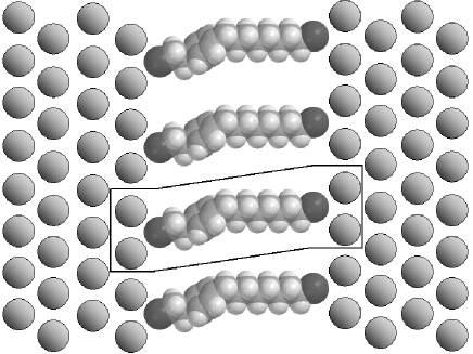
The electrode-MR-electrode junction is shown in Fig. 3. The equilibrium structure of isolated molecules was obtained through total energy minimization with the density-functional program Spartan [13]. An important factor affecting the electrical properties of the junction is the local geometry of the molecule-electrode contact. It is generally accepted that, upon self-assembly on gold, thiols lose the end hydrogens and then bind directly to the gold atoms. The preferential binding position of sulfur atoms on the Au(111) surface is at the apex of the pyramid with a triangular base of gold atoms (hollow position). Also possible is the top position, where the sulfur is positioned directly above one of the gold atoms [12]. In this paper, we assume the hollow binding position of the sulfur. In the hollow position, the end S states strongly hybridize with states on gold atoms, and the resulting current is less dependent on exact molecule-contact geometry in comparison to the top position[19]. Starting with the equilibrium molecular structure we remove the end hydrogens and replace them with two clusters of three gold atoms. The clusters form -bonds to sulfurs instead of the lost hydrogens. The primary molecule axis is roughly perpendicular to the planes of the gold triangles. The resulting molecular complexes (three gold atoms – dithiolate – three gold atoms) are organized in a periodic two-dimensional film which is placed between two (111) surfaces of semi-infinite gold electrodes. The film is commensurate with the Au(111) surface but its primitive surface cell is four times larger.
In order to obtain the I-V characteristic of the device we use the Landauer formulation of quantum transport [14] together with a semi-empirical tight-binding parameterization of the Hamiltonian matrices for the molecule and the electrodes. The off-diagonal matrix elements of the molecule are taken from Harrison [15]. They all are Slater-Koster linear combinations [16] of the four basic elements
| (7) |
where is the distance between atoms and , and , , and . The diagonal matrix elements, that is on-site energies of core atomic orbitals, are also adopted from [15], while the on-site energies of valence orbitals are calculated from atomic affinities and ionization potentials as discussed in [19]
| (8) |
The affinity and ionization potential determine the atomic Hubbard parameter as well:
| (9) |
Table I lists the molecular tight-binding parameters used in this paper.
| (eV) | (eV) | U (eV) | Number of electrons | |
|---|---|---|---|---|
| C | -6.91 | -17.52 | 8.7 | 4 |
| H | -7.85 | – | 11.5 | 1 |
| S | -20.80 | -6.47 | 7.8 | 6 |
| Au | -5.88 | – | 6.7 | 1 |
Our parameterization for the electrodes is based on the parameter sets of Papaconstantopoulos [17]. Although our calculational procedure enables us to treat the leads with the full set of , , and orbitals [18, 20], for the purposes of this paper the details of the electrode electronic structure are not important. We therefore choose to work with the component of the band structure only. The parameter of Ref.[17] for gold is eV. We found, however, that this value results in too narrow a band with the high-energy edge being not very far from the conducting LUMO of MR. In order to separate molecular rectification from the specific effects associated with gaps in the leads’ density of states, we also used the double value, eV. The same value of is used for matrix elements inside the electrode and between the electrode surface and atomic triangles that are part of the molecules. A comparison of the results obtained using the two values of will be given in Section IV. The second important parameter is the Fermi energy of the electrodes (that is minus the work function of the lead material). The effectiveness of our rectification mechanism depends critically on . Therefore we choose to study a series of which imitates the effect of using different electrodes. In particular, we studied the six values , , , , , and eV.
Calculation of current is performed utilizing a multi-step procedure. First, an isolated molecular complex (three Au atoms – dithiolate – three Au atoms) is treated as follows. The molecular Hamiltonian is constructed from the parameters described above. Then the molecular wave functions and their energies are found by diagonalizing the matrix . From the wave functions, the average number of electrons on each atom is calculated:
| (10) |
where the index numbers the molecular orbitals and the atomic orbitals that belong to atom . After that the diagonal matrix elements of (the onsite energies are recalculated as
| (11) |
where is the atomic charge of the -th atom, which in turn changes the charges on the atomic sites. Then the procedure is repeated until the charges converge. The converged charges define the final position of the molecular levels and the molecular Hamiltonian to be used in the transport calculations.
In the second step, the semi-infinite electrodes are solved. In our approach, there are two global quantum numbers, total energy and momentum parallel to the surface . Fixing converts the semi-infinite three-dimensional problem into a semi-infinite one-dimensional problem with a finite dimensional basis. Notice, however, that the Hamiltonian of the one-dimensional wire explicitly depends on . Thus transport problems at different are not equivalent. Moreover, the dependence on this quantum number could be substantial. It is important therefore to consider a grid of and the grid should be as dense as possible. Then we follow the procedure of Ref. [20], modified for the presence of an arbitrary oriented surface. For each and , we solve the channel problem, i.e. find all the Bloch vectors with both real and complex vectors. The former correspond to open conducting channels while the latter to evanescent channels. The wave functions and values of the channels are used to construct the surface Green’s functions of the electrodes. Note that no energy or momentum integration is required with this method.
On the next step, the molecule is eliminated from the picture by first solving the Schrödinger equation for the molecular wave function and then substituting the solution into the Schrödinger equation for the surface atoms of the leads. As a result of such a procedure, a matrix operator appears that directly couples states on the left wire with the states on the right wire. is essentially the inverse of convoluted with the matrices that describe the molecule-electrode coupling. Therefore, it contains all the information about the molecule. In particular, has poles at the energies of the molecular orbitals. Knowing and the Green’s functions of the free electrodes, the full electrode Green’s function is found from the Dyson equation [20]
| (12) |
where is the block-diagonal matrix in which the upper left corner is the free surface Green’s function of the left wire and the bottom right corner is that of the right wire. Note that the size of all the matrices involved in Eq. (12) is equal to the combined dimension of the left and right electrode surfaces. In the present study, each surface unit cell has four states, therefore all the matrices are .
Since the Green’s function solves Schrödinger’s equation for non-coincident spatial arguments, the transmission coefficients between the open channels can be found by multiplying by certain projector vectors . Each projection recovers an incident wave in one of the open channels in a particular electrode. The components of the vector determine the transmission and reflection amplitudes in all the open channels of both electrodes [20]. The contribution to current is found by squaring the transmission coefficients and summing over the open channels of the receiving wire. The total current is obtained by summing over all the incident channels available, then over , and integrating over energy :
| (13) | |||||
| (14) |
In the present study, we have used a grid of 64 points uniformly distributed over the two dimensional surface Brillouin zone.
An important and technically difficult problem is to account for the additional charge that the molecule acquires due to the mismatch of its equilibrium chemical potential with the Fermi energy of the electrodes. All the molecular components of the scattering wave functions could be found from the same Green’s function (12). Squaring them and integrating over energy, one finds new charges on the molecule, much like Eq. (10). Then the new on-site molecular energies are computed according to Eq. (11). Thus in principle, the entire calculational procedure described above (except the final calculation of current) has to be repeated many times until the charges converge. Moreover, this self-consistent procedure has to be performed anew for every value of the external bias voltage , i.e. out of equilibrium. The charges in this non-equilibrium case can be calculated with the use of the procedure described in [19].
The additional charge transfer is most important for strong coupling between the molecule and the wires. In this case, the molecular levels broaden significantly so that their tails can accommodate significant additional charge. Luckily, our rectification mechanism works best for narrow molecular resonances. As long as the Fermi energy remains below the conducting molecular level, the additional charge is negligible. For this reason, we do not perform the self-consistent calculation of charge in this paper. What we do take into account is the linear shift of the on-site atomic energies due to the external electric field due to the bias voltage.
IV Results

We begin by presenting our numerical results for the electrode density of states (DOS), see Fig. 4. Clearly visible are the square root singularities, which are characteristic of one-dimensional conductors. Recall that fixing renders the wire one-dimensional and the three-dimensionality is restored upon summation over the infinite number of points. The comparison of the main panel and inset in Fig. 4 indicates that this is indeed the case. Our choice of 64 points is a reasonable compromise between the accuracy and time for the transport calculations. The DOS affects the I-V characteristic of the diode in two ways. First, it changes the effective resonance width since . Thus, in the case of eV, the resonances are expected to be twice as narrow as for eV (.) Secondly, gaps/edges in the density of states could block elastic tunneling completely, resulting in a strong negative differential resistance effect. This possibility is discussed in Subsection (iv) below.
We investigated four major effects of the spatial and electronic structure of the junction on its I-V characteristic.
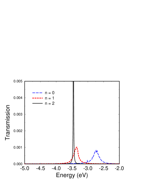
(i) Effect of the width of the molecular level on the rectification property of the junction. Within our mechanism, good rectification requires narrow molecular resonances. If the levels are narrow, the current rises steeply upon reaching the threshold voltage. In other words, there is very little current before the resonance is reached but some finite current after, which can produce a high rectification ratio. In the case of a broad resonance, the Lorentzian tails of the transmission function provide a sizeable current even before the nominal threshold voltage is reached. The rectification ratio should be small in this case. The width of the resonance is controlled by the thickness of the shorter insulating barrier. In Fig. 5 we compare the transmission function for the three molecular rectifiers which have no, one, and two insulating -CH2- groups on the short side. One can see that in the first two cases the resonance has a sizeable width of 0.2 eV (full width at half maximum), which implies strong coupling to the electrode. This is more or less obvious for , when the sulfur atom is directly attached to the benzene. The lone electron pair of the sulfur overlaps with the electrons of the ring, resulting in a molecular orbital distributed almost evenly over the ring and the sulfur. Since the sulfur is directly coupled to the electrode (albeit through an intermediate triangle), the molecular orbital is significantly broadened. In the rectifier, the sulfur is separated from the ring by a single insulating -CH2- group. However, because of the hybridization of carbon, the sulfur atom is out the plane of the ring. Then the separation between the sulfur and the ring is not large enough to prevent elongated -orbitals of sulfur and carbon from direct overlapping. As a result, the electronic level is still significantly broadened. The situation changes radically for . Two insulating groups move the sulfur away from the ring by 4.3 Å, so that direct overlap between the sulfur and the ring wave function becomes small. (From this point, insertion of new groups results in an exponential decrease of overlap.) According to our calculations, for the width is just meV, see Fig. 5.
The numerical results illustrate the general formula for transmission probability , Eq. (4). For the present molecular diodes, one partial level width is much larger than the other, say . Then transmission at the resonance is . Thus, as decreases due to better insulation, the resonance gets narrow but higher. For the diode, the resonance is narrow enough to be comparable with thermal, disorder, and other types of broadening present in the system. Further increase of the short barrier is unnecessary, it will result only in reducing the molecular asymmetry and spoiling the rectification property. Our conclusion from this analysis is that two -CH2- groups on the short side is the optimal choice for rectification. One should add that this rule has been derived for thiol-terminated molecules that are self-assembled on gold or other noble metal. For other types of contact, this may change. For instance, when an LB film is deposited on a metallic surface, a larger (Van-der-Waals-like) gap may exist between the film and the metal. Such a gap will serve as an additional insulator, which may reduce the optimal length of insulating material on the molecule itself.

(ii) Effect of the metal work function on the forward and reverse voltages. According to Eqs. (2) and (3), the forward and reverse voltages are directly proportional to the equilibrium energy difference between the conducting molecular level and the Fermi energy of the metal. We have studied this effect by varying the electrode Fermi energies with respect to the molecular orbitals. The results are presented in Fig. 6 and in Table II. The I-V characteristics all have similar shape but their forward and reverse voltages systematically increase with , as expected. Analysis of parameters from Table II reveals that the ratios , , and all remain approximately constant as functions of for and . Thus the ratio is independent of electrode material and is indeed a characteristic of the molecule asymmetry only. However, the relation is satisfied only approximately. For the (2,6) molecule, presented in Fig 6, which is almost twice the voltage ratio. This is because the simple equations (2) and (3) do not take into account the voltage drop on the central conductive unit. Clearly, some voltage always drops there, which effectively increases the lengths of both barriers and reduces the anisotropy. We discuss this issue in more detail in subsection (iii) below.
| (eV) | (eV) | (V) | (V) | (V) | ||
|---|---|---|---|---|---|---|
| 4.0 | 0.55 | 0.90 | 1.44 | 1.60 | 1.13 | 56 |
| 4.2 | 0.75 | 1.19 | 1.93 | 1.62 | 1.41 | 118 |
| 4.5 | 1.05 | 1.66 | 2.73 | 1.64 | 2.07 | 173 |
| 5.0 | 1.55 | 2.51 | 4.01 | 1.60 | 3.02 | 276 |
| 5.2 | 1.75 | 2.77 | 4.50 | 1.63 | 3.68 | 305 |
| 5.5 | 2.05 | 3.25 | 5.32 | 1.64 | 4.25 | 323 |
The last two columns of Table II present data on current rectification. As a measure of the latter, we choose to compare currents at some positive and negative voltages with the same absolute value . Obviously, rectification is strongest if is chosen between and . In this case, in the positive direction there is already some appreciable current due to resonant tunneling through the molecular level. In the reverse direction, the tunneling is still under barrier and therefore is exponentially reduced. This is the essence of our rectification mechanism. The values of the operating voltage shown in the table are roughly halfway between and . (Approximately, .) One can see that the current ratio is a steadily increasing function of . The overall dependence is close to linear, with both end points being slightly off this general trend.
An interesting problem is choosing an optimal value of . As we have seen, large s result in better rectification of current and wider rectification voltage windows . The latter fact is very important because all sorts of disorder in the system will tend to shrink the working window. Also, a particular circuit design may require the operating reverse voltage must be larger in absolute value than a certain voltage. In general, the absolute value has to be as large as possible. Both these arguments favor a large . On the other hand, large operating voltages imply higher power and higher electrostatic stress on the molecules, which are, of course, undesirable. Quantitative understanding of this trade off problem warrants a detailed investigation for a particular application.

(iii) Effect of the length of the insulating barrier on the asymmetry of the I-V characteristic and on the overall current magnitude. This effect is central to the present paper. By increasing the length of the longer barrier while keeping the shorter one fixed, one forces a larger portion of the voltage to drop on the longer barrier. This implies that the conducting threshold is reached at different bias voltages in the two opposite directions, as illustrated in Fig. 2. This design principle provides us with the means to systematically increase the current rectification ratio and produce better molecular diodes. In Fig. 7, we show the calculated I-V characteristics of a series of molecular diodes for work function eV. The electrical parameters of the I-V characteristics are summarized in Table III. The series begins with the symmetric molecule , which produces a symmetric I-V characteristic with V. With increasing , monotonically decreases but increases, resulting in a systematic shift of the I-V characteristic with respect to the origin. By , the reverse-to-forward voltage ratio reaches . The voltage ratio grows slower than , suggested by Eqs. (2) and (3). It could be described by the relation
| (15) |
where is a correction that takes into account the voltage drop on the central conducting unit. Using the data of Table III, one finds , 4.0, 4.0, and 4.9 for , 6, 8, and 10, respectively. The correction does not remain constant as a function of . Therefore it is difficult to assign to it a useful geometrical meaning.
The penultimate column of Table III shows the current rectification ratios . It grows approximately proportional to , reaching a value of at .
| (V) | (V) | (V) | ||||
|---|---|---|---|---|---|---|
| 2 | 1.19 | 1.19 | 1.00 | any | 1 | 0.33a |
| 4 | 0.99 | 1.28 | 1.29 | 1.13 | 32 | 2.40 |
| 6 | 0.90 | 1.44 | 1.60 | 1.13 | 56 | 42.6 |
| 8 | 0.81 | 1.61 | 1.99 | 1.13 | 76 | 836 |
| 10 | 0.80 | 1.74 | 2.18 | 1.13 | 104 | 13,150 |
a resistance at V.
The important issue is the exponential growth of the diode resistance with , see the last column of Table III. This result is, of course, expected because the transmission as well as the current through the molecule is directly proportional to , see Eqs. (4) and (6) at . As the barrier length increases, the probability of underbarrier tunneling goes down exponentially fast, which is reflected in the numerical data. According to our calculations, addition of every extra pair of -(CH2)- groups increases the resistance by a factor of . [Note that for the transition should not follow the same trend because at the molecule is symmetric and .] Thus we have an unfavorable trade off problem where the rectification ratio improves linearly with but the resistance and the time constant of the device worsens exponentially. This is an inherent feature of our mechanism and in some sense the price for its simplicity. When discussing the rectifier resistances, one should not forget that what matters is the total resistance of an electronic element. With a typical target size of nm2, the number of molecules per junction is going to be of order of 1000. Then even and 10 diodes will have total resistances of 1-10 M, which amounts to a time constant for a m long nanowire, and for a 1 cm long nanowire.
| (eV) | 4.0 | 4.2 | 4.5 | 5.0 | 5.2 | 5.5 |
|---|---|---|---|---|---|---|
| (eV) | 0.55 | 0.75 | 1.05 | 1.55 | 1.75 | 2.05 |
| (1,2) | 4a | 5b | 8c | 12d | 39 | 56 |
| (1,4) | 10a | 13b | 26c | 75 | 111 | 154 |
| (1,6) | 15 | 25 | 44 | 112 | 127 | 152 |
| (1,8) | 16 | 25 | 44 | 91 | 143e | 126 |
| (1,10) | 19 | 27 | 47 | 85 | 123 | |
| (2,4) | 32 | 52 | 91 | 138 | 156 | 154 |
| (2,6) | 56 | 74 | 173 | 276 | 374 | 444 |
| (2,8) | 76 | 92 | 225 | N/C | 438e | N/C |
| (2,10) | 104 | 118 | 290 | N/C | 556e | N/C |
| (V) | 1.13 | 1.51 | 2.08 | 3.02 | 3.50 | 3.97 |
a at V.
b at V.
c at V.
d at V.
e at V.
The data from Table II suggests that rectification could be improved further by increasing the initial energy difference . We computed I-V characteristics for every value of the work function listed in Table II and for all MRs with and . [In addition, everything was calculated for the two values of the electrode matrix element , bringing the total number of studied I-Vs to 120.] All the curves have shapes similar to those in Figs. 6 and 7, therefore we do not show them explicitly. Table IV summarizes the results on rectification ratios for a variety of combinations. As expected, the rectification ratio grows with both and . The maximum ratio of above 500 was observed for and eV ( eV).
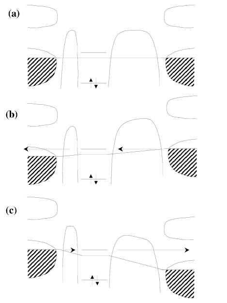
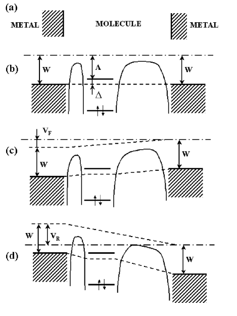
(iv) Role of energy gaps in the electrodes’ density of states. This effect is not generic and potentially applies to semiconductor electrodes only. Nevertheless, it offers an interesting possibility to enhance the rectification property of the diode by inhibiting current flow in the reverse direction due to an energy gap in the density of states. The basic idea is illustrated in Fig. 8. At some voltage , the bottom of the gap aligns with the conducting molecular orbital. At higher resonant tunneling becomes impossible due to the lack of available final electronic states. Accordingly, the current must drop to zero at . If lies in between and , then there will be some substantial current in the forward direction in the interval , Fig. 8(b), while no current at all in the reverse direction, Fig. 8(c). In the latter case, the gap of the right electrode is reached before the left Fermi energy aligns with the conducting orbital.

The above argument does not take into account inelastic processes. If included, they would result in a non-zero current even in the situation of Fig. 8(c). In this case, the electrons can tunnel under the right barrier with irradiation of phonons, arriving at the right electrode with a reduced energy for which there are available states at the top of the valence band. In this paper we assume that the elastic tunneling is the dominant transport mechanism and such processes can be neglected. We have modeled this effect by using the smaller electrode matrix element eV. Typical I-V characteristics are shown in Fig.9 and their parameters are summarized in Table V. With increasing (and ), the forward and reverse voltages and increase in accordance with Eqs. (2) and (3). At the same time, decreases because the bottom of the energy gap moves closer to the conducting molecular level. As a result, the window of resonant tunneling is squeezed from both sides and at some critical vanishes altogether. This effect can be seen in Fig.9. In the reverse direction, the peak disappears between eV and eV. In the forward direction, the same happens between eV and eV. (Of course, resonant tunneling survives longer in the forward direction because .)
| (eV) | (eV) | (V) | (V) | (V) | (V) | |
|---|---|---|---|---|---|---|
| 4.0 | 0.55 | 0.84 | 1.62 | N/C | 1.23 | 70 |
| 4.2 | 0.75 | 1.17 | 2.16 | N/C | 1.80 | 151 |
| 4.5 | 1.05 | 1.58 | N/C | 5.20 | 2.17 | 282 |
| 5.0 | 1.55 | 2.33 | N/C | 3.68 | 2.83 | 1308 |
| 5.2 | 1.75 | 2.60 | N/C | 3.10 | 2.83 | 1064 |
| 5.5 | 2.05 | N/C | N/C | N/C | 2.83 | 3 |
Notice that the I-Vs of Fig. 9 display large negative differential resistance under positive bias. In this respect, our molecular diodes behave similarly to the conventional semiconducting tunneling diodes. However, under negative bias, the behavior is quite different. While the tunneling diodes conduct very well under reverse bias, our MR conduct very little.
V Conclusions
The major purpose of this paper has been to predict several trends in the I-V characteristics of MR when they are dominated by resonant tunneling through a certain molecular orbital localized on the conjugated part of a spatially asymmetric molecule. To achieve a large rectification ratio, the conjugated part of the molecule must be connected to electrodes by insulating molecular groups of different length. By varying the ratio between the barrier lengths, one can achieve a rectification ratio of several hundred while keeping the current through the molecule at measurable levels.
As far as the described mechanism of molecular rectification is concerned, the observed trends could be divided into “spatial” and “energetic” domains. The spatial trends refer to the changes in the I-V characteristic that follow from changing the lengths of the two insulating barriers of the MR. The length of the shorter barrier controls the width the molecular resonance. We have found the optimal length to be two -(CH2)- groups. One such group does not provide sufficient insulation of the conducting unit from the metal. As a result, the resonance is too broad and current asymmetry is not pronounced. More than two -(CH2)- groups make the resonance narrower than temperature and disorder induced widths, which is not useful. Increasing the length of the longer barrier improves the current rectification ratio but increases the total resistance of the molecular diode. These trends can be observed experimentally by studying several molecules with different lengths of the longer chain but identical otherwise. The energetic trends refer to the dependence of the rectification property on the work function of the electrode material and on the electron affinity of the molecule. The two quantities define the parameter , which is the most important energy scale in the problem. In general, larger leads to better rectification but at the same time to larger operating voltages. These trends can also be checked experimentally by measuring, for instance, the same molecule on gold and silver electrodes, or by measuring the molecules with different conducting units (say, benzene and naphthalene) on the same set of electrodes.
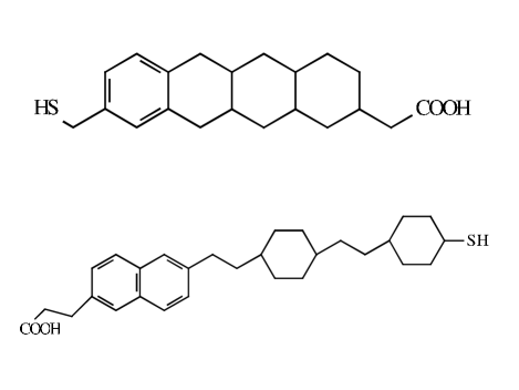
Most of our results are rather insensitive to changing the end (“anchor”) groups. The role of the latter is to provide better connection to the electrodes. Thus the end groups could be adjusted to the particular experimental setup without significantly altering the electrical properties of the device. They could even be absent altogether if the measurement technique does not require covalent bonding between the molecules and the electrodes. The composition of the insulating barriers may be changed too. For instance, instead of alkane chains one could use a combination of the alkane segments and saturated cyclic hydrocarbons, see Fig. 10. An advantage of this design is that the molecules have more or less the same cross section along their entire length. Therefore the packing of the film will be much better. On the other hand, such MR could be harder to synthesize.
These conclusions are certainly limited to the particular set of approximations used in the present study. For instance, we have ignored inelastic processes, which should become progressively more important for larger molecules and at larger bias voltages. Inelastic scattering generally increases the current through the system, since the carrier has more final states to tunnel into when it can lose energy by exciting a vibronic excitation. In the present resonant case, when exceeds the threshold, either or , there will be some electrons with energy higher than the energy of the LUMO resonance. Such electrons can still tunnel through the junction effectively by first loosing their energy and then tunneling resonantly. Thus the overall current will continue to grow after the initial sharp increase, in contrast to the elastic-only case where the current stays approximately constant. Additionally, a finite temperature should smoothen the sharp features of the I-V characteristic, thereby reducing the rectification ratio. The inclusion of inelastic processes would probably reduce the estimated rectification ratio.
In conclusion, we have described a simple principle for molecular rectification. It requires only one conducting molecular level located asymmetrically with respect to the electrodes. Theoretical calculations have shown that current rectification ratios of several hundred are achievable with this mechanism. Higher ratios are likely to be accompanied by a significant reduction in conductance, which will make such diodes less practical. We have made several predictions of how the rectification properties should change between different molecules and different electrode materials (work functions). These trends are experimentally verifiable on families of structurally similar molecules. Such trends are signatures of resonant tunneling through molecules and could serve as proof of experimental observation of the latter.
REFERENCES
- [1] A. Aviram and M. A .Ratner, Chem. Phys. Lett. 29, 277 (1974).
- [2] A. S. Martin, J. R. Sambles, and G. J. Ashwell, Phys. Rev. Lett. 70, 218 (1993).
- [3] R. M. Metzger, B. Chen, U. Höpfner, M. V. Lakshmikantham, D. Vuillaume, T. Kawai, X. Wu, H. Tachibana, T. V. Hughes, H. Sakurai, J. W. Baldwin, C. Hosch, M. P. Cava, L. Brehmer, and G. J. Ashwell, J. Am. Chem. Soc. 119, 10455 (1997).
- [4] C. Zhou, M. R. Deshpande, M. A. Reed, L. Jones II, and J. M. Tour, Appl. Phys. Lett. 71, 611 (1997).
- [5] J. C. Ellenbogen and J. C. Love, Proc. IEEE 88, 386 (2000).
- [6] C. Krzeminski, C. Delerue, G. Allan, D. Vuillaume, and R. M. Metzger, Phys. Rev. B 64, 085405 (2001).
- [7] R. M. Metzger, J. Mater. Chem. 9, 2027 (1999).
- [8] C. Boulas, J. V. Davidovits, F. Rondelez, and D. Vuillaume, Phys. Rev. Lett. 76, 4797 (1996).
- [9] Y. Xue, S. Datta, S. Hong, R. Reifenberger, J. I. Henderson, and C. P. Kubiak, Phys. Rev. B 59, 7852 (1999).
- [10] A. W. Ghosh, F. Zahid, P. S. Damle, and S. Datta, cond-mat/0202519.
- [11] J. Reichert, R. Ochs, D. Beckmann, H. W. Weber, M. Mayor, and H. v Löhneysen, cond-mat/0106219.
- [12] H. Sellers, A. Ulman, Y. Shnidman, and J.E.Eilers, J. Am. Chem. Soc. 115, 9389 (1993).
- [13] SPARTAN version 5.0, Wavefunction, Inc. 18401 Von Karman Avenue, Suite 370, Irvine, CA 92612 U.S.A.
- [14] Y. Imry, Introduction to mesoscopic physics (Oxford Univ. Press, New York, 1997); R. Landauer, IBM J. Res. Dev. 1, 223 (1957); Phys. Lett. 85A, 91 (1981).
- [15] W. A. Harrison, Electronic Structure and the Properties of Solids (Dover, London, 1989).
- [16] J. C. Slater and G. F. Koster, Phys. Rev. 94, 1498 (1954).
- [17] D. A. Papaconstantopoulos, Handbook of the Band Structure of Elemental Solids (Plenum, New York, 1986).
- [18] P. E. Kornilovitch and A. M. Bratkovsky, Phys. Rev. B 64, 195413 (2001).
- [19] A.M. Bratkovsky and P.E. Kornilovitch, cond-mat/0204597 (2002).
- [20] S. Sanvito, C. J. Lambert, J. H. Jefferson, and A. M. Bratkovsky, Phys. Rev. B 59, 11936 (1999).