Scanning tunnelling spectroscopy of electron resonators
Abstract
The electronic structure of artificial Mn atom arrays on Ag(111) is characterized in detail with scanning tunnelling spectroscopy and spectroscopic imaging at low temperature. We demonstrate the degree to which variations in geometry may be used to control spatial and spectral distributions of surface state electrons confined within the arrays, how these are influenced by atoms placed within the structure and how the ability to induce spectral features at specific energies may be exploited through lineshape analyses to deduce quasiparticle lifetimes near the Fermi level. Through extensive comparison of maps and spectra we demonstrate the utility of a model based upon two-dimensional -wave scatterers for describing and predicting the characteristics of specific resonators.
I Introduction
A central aim of nanoscale science is to controllably modify material properties on a nanometre scale. One of its greatest achievements has been manipulation of surface atomic structure with the scanning tunnelling microscope (STM) Eig_Nat90 , and some of the most striking demonstrations of this capability the construction of complex arrays of adatoms by the maneuvering and positioning of individual adatoms Cro_Sci93 . Synthesized nanoscale structures such as these, as well as other surface nanostructures including islands Avo_Sci94 ; Li_PRL98_2 and step arrays Bur_PRL98 act as resonators for mobile surface electrons, with characteristics that may be controlled by the adjustment of geometrical parameters.
Here we present a detailed analysis of the electronic structure of a particular class of resonator, surface nanocavities constructed from Mn atoms on Ag(111). Of particular interest is the extent to which a simple scattering model, which takes into account the atomic structure of the resonator, can successfully describe its spatial and spectral electron distributions. Recent work agmn:prl has shown that the specific characteristics of individual resonators impact upon the electronic structure of adsorbates positioned within them, and may open up the possibility of atomic scale control of magnetic or chemical properties.
In addition, we consider the use of these artificial nanoscale structures for probing quasiparticle lifetimes close to the Fermi energy. The lifetimes of excitations enter the description of many important surface phenomena such as the dynamics of charge and energy transfer, and for excitations in surface bands reflect a complex combination of decay processes via both surface-localised and extended states, with the additional influence of screening that varies rapidly as the electron density decreases outside the surface. Successful prediction of lifetimes remains an on-going theoretical problem ECHE , whilst measurements must overcome considerable challenges (reviewed in Ref. Matzdorf_SSR98 ) so that only recently Kliewer_Science00 has a consistent account of the lifetime of a prototype quasiparticle, a hole in a surface band, been constructed, based upon tunnelling spectroscopy at the surface state band edge on noble metal (111) faces Li_life . The spatial decay of electron interference patterns observed in STM images provides an alternative approach first indicated by Avouris PROPO , and has been used to measure lifetimes well removed from the Fermi energy Buergi_PRL99 . However, lifetime measurements for states close in energy to are still lacking but are of particular interest because the relative contributions of phononic and electronic decay channels are expected to change significantly in this range. We indicate how electron resonators may be used for this purpose.
II Methods
II.1 Experimental Procedures
We study nanocavities constructed using Mn adatoms on the Ag (111) surface in a custom-built ultra-high vacuum (UHV) STM, operating at a temperature of K kliewerdiss . The Mn atoms were evaporated onto a cold Ag substrate that had been prepared by standard procedures in UHV. Electrochemically etched W tips were prepared in UHV by sputtering and annealing. Differential conductivity () spectra were recorded under open feedback loop conditions using a lock-in amplifier with a sinusoidal modulation added to the sample bias. Moreover, maps of were recorded simultaneously with constant current imaging without opening the feedback.
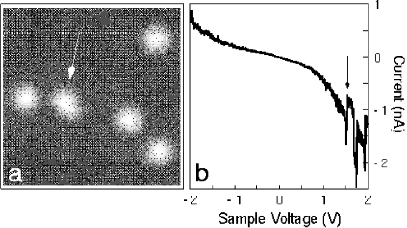
Manganese atoms on Ag(111) image as Å high and Å wide protrusions (full width at half maximum) at a sample voltage V (Fig. 1a), similar to previous observations of adatom species on noble metal surfaces Cro_Sci93 ; Cro_PRB93 . Most of the STM images presented here have been recorded at V and a tunnelling current nA, i.e. a tunnelling resistance G; these values are chosen because the tip-sample interaction is sufficiently strong for below M that atoms are occasionally moved during scans, as demonstrated in Figure 1a. In spectroscopy of single Mn atoms we observe abrupt current changes at V and G, Figure 1b, indicating the onset of induced atomic mobility. To achieve acceptable signal-to-noise ratios in tunnelling spectroscopy elevated modulation amplitudes were required ( mVpp).
We construct artificial structures via controlled relocation of individual Mn atoms, using a sliding process pioneered by Eigler Eig_Nat90 . A Mn adatom is moved by placing the tip over the atom at large tip-sample separation (typically G), reducing this separation ( V, M) and then moving the tip slowly across the surface (a rate of one lattice constant per second) to the desired location. The adatom follows the tip motion, and is left in position by retracting the tip.
II.2 Modelling
To model the experiments it is important to take into account the constant-current mode of operation that is used in obtaining the maps. The tunnelling current is calculated as Selloni_PRB85
| (1) |
where is the local density of states (LDOS) of the sample at the position of the tip and where the transmission probability is given by
| (2) |
with tip-sample distance and workfunctions eV and eV of tip and sample respectively Mic_JAP77 . Simulating the feedback loop, was adjusted for each lateral position () to ensure constant current , which in turn was numerically differentiated to obtain . In using (1) we assume an electronically featureless tip, which is supported by the absence of any tip dependence to be seen during the experiments.
For we consider an array of two-dimensional -wave scatterers with coordinates , . This is the model introduced by Heller et al Hel_Nat94 . We determine from the Green function
| (3) |
which is given by multiple-scattering theory in terms of the free-electron Green function economou
| (4) |
where and the -matrices that characterise the point scatterers:
| (5) | |||||
| (6) |
A number of parameters enter the calculations. We use -matrices corresponding to perfectly absorbing scatterers, as identified by Heller et al. Hel_Nat94 and used by them to describe the spectrum of a 60 Fe atom corral on Cu(111). This boundary condition reflects the strong coupling to bulk states Cra_PRL94 that occurs at the adatoms. The effective mass and surface state band edge meV have been determined previously Li_PRB97 ; Kliewer_Science00 . The positions of the atoms and the lateral position of the tip are crucial in determining the exact shape of spectra. For example, only the highest symmetry eigenstates contribute at the centre of a circular structure, but slightly off centre or if the shape is not exactly regular a mixing of state occurs, giving additional structure. Uncertainty enters these coordinates through the piezo calibration and possible anisotropy of the piezo sensitivity in the fast () and slow () scanning directions. Therefore an optimisation scheme was used based upon a fit using the Levenberg-Marquardt method in which the relative coordinates were fixed but independently scaled in the and directions. After the initial determination, the piezo calibration parameters were held fixed in all subsequent calculations. In a second stage, the calculations have been extended further to include an energy dependent lifetime of the electronic states (Sect. III.4). This was accomplished via a parameterised imaginary self energy added to the energy in computing from equations (4)-(6). The importance of the self energy in determining the peak amplitudes and widths in the LDOS has been noted previously Cra_PRL94 ; Cra_PRB96 . Here we exploit this dependence to extract from experimental data.
III Results
III.1 28 atom rectangle
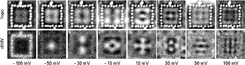
Figure 2 displays data from an array of Mn adatoms. Images a–h are constant current topographs covering a range of different voltages, recorded at values indicated in the figure. The adatoms, which appear as bright protrusions in every case, have been arranged into a rectangular geometry with approximate dimensions of Å2. Inside this structure a weak corrugation is found, originating from the confinement of the surface state electrons. A nonlinear height scale has been used for display, in order to render this weak corrugation easily discernible; this has the side effect that the adatoms appear rather blunt. At negative voltages (i.e. when tunnelling from occupied levels in the sample) the constant current topographs exhibit a rectangular pattern of four maxima within the confining array of Mn atoms, which is still discernible at voltages well below the bottom of the surface state band at meV. This pattern persists owing to the preferential tunnelling from occupied states at the Fermi level. At positive voltages, imaging unoccupied states, the pattern becomes more complex and varies with , the most significant tunnelling now occuring at energies corresponding to the varying bias voltage.
Images i–p show maps that were recorded simultaneously with the topographic scans. Below , the adatoms cause clear features, whereas no corrugation is discernible inside the array. In contrast, above a clear wave pattern arises within the structure, while the adatoms are only weak features which conveniently serve to indicate the rectangular boundary. The evolution with energy of the internal pattern is as expected, representing a progression through the nodal structures of the lowest lying “particle-in-a-box” eigenstates of the rectangular cavity, where and are the linear dimensions of the structure. At low energy, Fig. 2j, a single maximum occurs (). Next, two maxima appear along the longer axis of the rectangle (Fig. 2k), corresponding to the level. The mV map (Fig. 2l) showing four maxima, two along each axis of the rectangle, reflects contributions from both the second () and third () levels. The states are in reality resonances that in general overlap in energy, so that maps can contain contributions from several. At higher energies, the pattern becomes increasingly complex.
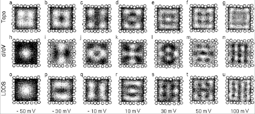
Calculated results are displayed in Fig. 3 where panels a–g are topographs, h–n are maps and o-u are LDOS maps. Close inspection and comparison with Figs. 2b-h, and 2j-p reveals that the experimental features are reproduced well by the model calculations. As pointed out previously Li_PRB97 , experimental data recorded by the methods used here are affected by the variations in tip-sample separation which give rise to the corrugation in the topographs. Consequently maps are not directly comparable to LDOS maps, a fact clearly visible by comparing Figs. 3l and s, or 3m and t, although the similarity between the two tends to increase with increasing bias voltages. Indeed, around zero bias it is topographs and not that are are expected to resemble the LDOS, and this is clearly the case in Fig. 3.

A more detailed comparison between experiment and theory is possible in the case of spectra. An example measured near the centre of the rectangular resonator is shown in the left panel of Fig. 4. Tunneling from a -state tip directly at the centre of an ideal rectangular structure can only take place into surface state levels with odd quantum numbers . This is the origin of the large peaks at meV and between and meV. Irregularities in the structure and deviations in position of the tip from the the exact centre introduce additional weak tunneling channels, e.g. near meV, whilst the intrinsic width of the confined levels further modifies the spectrum. Comparing the measured spectrum with the LDOS calculated using the two-dimensional scattering model that includes the structural irregularities and correct tip position, displayed in the same panel in Fig. 4, we see the latter faithfully reproduces the differential conductivity spectrum. Note that the characteristic temperature associated with Kondo behaviour in Mn/Ag alloys is mK Flo_PRL70 and thus does not affect the line shape kondo under the present experimental conditions.
III.2 35 atom ring
We have also performed similar experiments and calculations on other geometries, such as adatom rings. The right panel of Figure 4 contains a comparison between the differential conductivity spectrum, measured approximately Å off centre in a Å diameter ring formed from 35 Mn adatoms, and the corresponding LDOS obtained using the -wave scattering model. The spectrum contains a large number of peaks, the off-centre position enabling low symmetry eigenstates to provide channels for tunnelling, but these are reproduced in the theoretical LDOS spectrum calculated using the precise atomic positions of the Mn ring. We conclude that the -wave scattering model provides an adequate basis for modelling the spatial and spectral electron distributions in electron resonators.
III.3 Adatoms in resonators
Having characterised the properties of electron resonators we have next investigated the interaction with an additional atom introduced into the nanocavity region. These structures were formed by maneuvering one of the boundary Mn atoms into the central region, and then moving a Mn atom elsewhere on the surface into the vacant position in the boundary, restoring the integrity of the resonator.
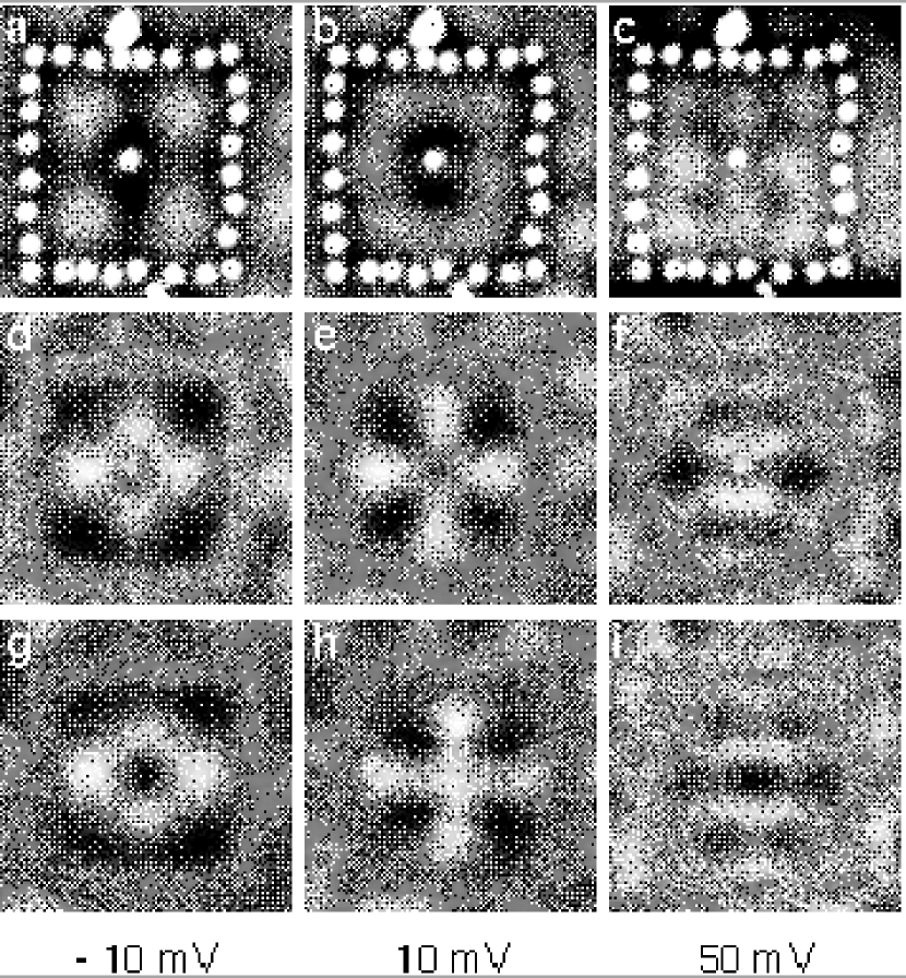
In Figure 5 we show maps of a rectangular structure made from 28 Mn atoms and measured at three different voltages, contrasting the images obtained with and without a Mn atom inside the structure. At first glance the presence of the central atom appears to barely affect the wave pattern inside the rectangle, apart from in the immediate vicinity of the centre atom. There, the difference is striking. At voltages of mV and mV where is at a minimum in the empty structure (Figs. 5g and i), exhibits a peak in the centre upon insertion of the atom (Figs. 5d and f). At mV, however, the maximum observed in the empty rectangle (Fig. 5h) changes to a minimum (Fig. 5e).
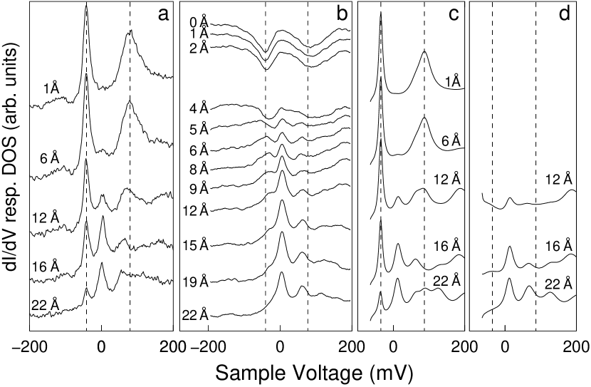
This “contrast reversal” has been previously reported and explained as a consequence of the strong hybridisation between states on the Mn atom and substrate surface electron levels agmn:prl , and has been reproduced in calculations of the local density of states directly on Mn atoms in resonators of various geometries using full three-dimensional multiple scattering calculations. Here we consider how this interaction extends away from the central Mn atom and the degree to which the two-dimensional scattering model describes the behaviour. Fig. 6 shows a series of spectra measured at various distances from the centre of an empty adatom ring, and when a Mn atom has been introduced. Also shown are the LDOS calculations for identical geometries. Comparing spectra in Figs. 6a and b at central positions closest to the location of the new adatom, it is clear that spectral peaks in the empty resonator coincide with troughs of the occupied structure (vertical dashed lines). This is evidence for strong hybridisation agmn:prl . Moving laterally away from this central position the characteristic peak structure of the empty resonator returns, with the exception of the lowest peak near mV which remains absent even at large displacements. This prominent feature is associated with a nodeless resonator eigenstate that has its maximum at the centre of the ring, and so is particularly sensitive to the introduction of a Mn atom into the central region.
The two right-most panels in Fig. 6 show the LDOS calculated for this system using the two-dimensional scattering model, at lateral positions at which spectra were recorded. The prominent features in the experimental spectra are reproduced well in the theoretical curves, again showing that the simple scattering model, using the exact atomic locations of the Mn atoms making up the structure, gives an accurate and valid account of the electronic structure of resonators. The calculations also confirm that the dominant state in the empty resonator is absent in the spectrum of states of the occupied resonator, so that the insensitivity of maps to the presence of the central atom away from its immediate vicinity that was suggested by Fig. 5 clearly does not extend to all sample voltages. Note that in Fig. 6d we have omitted theoretical spectra within Å of the central Mn atom. Within this radius (which is much greater than the topographic radius of the Mn atoms) the differential conductivity also has large contributions from channels involving bulk states scattered by the adatom buried , and these are not included in the model. Also omitted in the model is any spatial information about the adatom orbitals that would also be required to model spectra (and maps) in its immediate vicinity.
III.4 Energy dependent self energy
The basic idea of our approach to lifetime measurements is straightforward kliewerdiss . Exploiting the properties of the electron resonators identified in the previous sections we construct nanocavities with electronic features in the vicinity of . The lineshape of the spectral features are affected by lifetime-limiting processes so that through analysis the lifetime can be determined. By changing the geometry of nanoscale structures it is possible to tune the eigenstate energies of the structures, and thus generate states at various energies in order to obtain the energy dependence of the lifetime. The two-dimensional scattering model validated above enables the design of suitable structures. We note that a fully quantitative analysis will also require information on the energy dependence of the tip density of states, which is not expected to be constant over a wide energy range, and likewise the bulk density of states of the crystal which causes a background signal in spectra. Here, we seek to demonstrate the concept and so neglect these influences. Following Li et al. Li_life we describe the lifetime effects in terms of an effective imaginary part of the self energy, where .
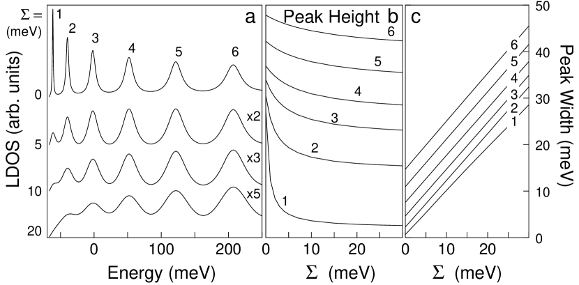
The effect of on the LDOS of an artificial nanoscale resonator is shown in Fig. 7a for a 210 Å diameter ring. The calculation for vanishing , i.e. infinite lifetime, yields a series of sharp resonances (Fig. 7a, top curve). Note that the spectrum corresponds to the centre of the structure. The high symmetry gives the “cleanest” spectrum, avoiding difficulties that exist at off-centre positions where resonances can overlap. With increasing there is a reduction of the peak heights and a concomitant broadening, especially apparent for the lowest of the states which have the sharpest intrinsic profile. These trends are quantified by fitting a series of Lorentzians to the data, and Figure 7b and c display the widths and height extracted through this analysis. As increases, the peak heights decrease monotonically, the lowest (in energy) peaks most rapidly, whilst there is an essentially linear dependence of the peak width on .

Figure 8 shows values of obtained from an analysis of measurements from two nanostructures. For each, fits were made over limited energy ranges ( meV) adjusting coefficients of a linear parameterisation of . We estimate the error of thus determined to be of the order of %. The diamonds and squares are derived from spectra for a 35 atom circular resonator, and the filled circles were obtained from a 16 atom circle. Below the Fermi energy () approaches a value obtained previously from spectra taken on clean terraces which yielded meV Kliewer_Science00 . There is a clear increase of at large energies, and we find eV meV, which is comparable with an extrapolation down to this energy of data for the Ag(111) surface state extracted from the spatial coherence of interference patterns at energies eV by Bürgi et al. Buergi_PRL99 . Finally, at energies close to we observe a marked decrease of which corresponds to an increased lifetime of the corresponding quasiparticles (inset in Fig. 8). Increased lifetimes are indeed expected as both the phononic and electronic decay channels become less efficient. While further data close to is necessary to quantitatively characterize this effect the first results are encouraging. Future work will also address the relation of the self-energies determined from atomic arrays to that of an unperturbed surface. We note that data from resonators of different diametres (40 Å and 115 Å) yield similar . This similarity appears to indicate that the influence of the array may be rather small.
IV Summary
Using scanning tunnelling spectroscopy and spectroscopic imaging at low temperature we have investigated artificial Mn atom arrays on Ag(111). These act as electron resonators and we have demonstrated the degree to which variations in geometry may be used to control spatial and spectral distributions of confined surface state electrons. This control may be exploited in manipulating the local density of states of adsorbates introduced into the resonator, or as we have demonstrated, to generate spectral features at specific energies in order to perform lineshape analyses from which quasiparticle lifetimes may be deduced. Extensive comparison of maps and spectra indicated the utility of a model based upon two-dimensional -wave scatterers for describing and predicting the characteristics of specific resonators.
Acknowledgements
This work has been supported the DFG, the DAAD and the UK EPSRC.
References
- (1) D. M. Eigler, E. K. Schweizer, Nature 344, 524 (1990).
- (2) M. F. Crommie, C. P. Lutz, D. M. Eigler, Science 262, 218 (1993).
- (3) Ph. Avouris, I.-W. Lyo, Science 264, 942 (1994).
- (4) J. Li, W.-D. Schneider, R. Berndt, S. Crampin, Phys. Rev. Lett. 80, 3332 (1998).
- (5) L. Bürgi, O. Jeandupeux, A. Hirstein, H. Brune, K. Kern, Phys. Rev. Lett. 81, 5370 (1998).
- (6) J. Kliewer, S. Crampin, R. Berndt, Phys. Rev. Lett. 85, 4936 (2000).
- (7) P.M. Echenique, J. Osma, V.M. Silkin, E.V. Chulkov, J.M. Pitarke, Appl. Phys. A 71, 503 (2000).
- (8) R. Matzdorf, Surf. Sci. Rep. 30, 153 (1998).
- (9) J. Kliewer, R. Berndt, E. V. Chulkov, V. M. Silkin, P. M. Echenique, S. Crampin, Science 288, 1399 (2000).
- (10) J. Li, W.-D. Schneider, R. Berndt, O. R. Bryant, S. Crampin, Phys. Rev. Lett. 81, 4464 (1998).
- (11) Ph. Avouris, I.-W. Lyo, R. E. Walkup, Y. Hasegawa, J. Vac. Sci. Technol. B 12, 1447 (1994).
- (12) L. Bürgi, O. Jeandupeux, H. Brune, K. Kern, Phys. Rev. Lett. 82, 4516 (1999).
- (13) J. Kliewer, PhD thesis, RWTH Aachen, D-52056 Aachen, Germany (2000).
- (14) M. F. Crommie, C. P. Lutz, D. M. Eigler, Phys. Rev. B 48, 2851 (1993).
- (15) A. Selloni, P. Carnevali, E. Tosatti, C. D. Chen, Phys. Rev. B 31, 2602 (1985).
- (16) H. B. Michaelson, J. Appl. Phys. 48, 4729 (1977).
- (17) E. J. Heller, M. F. Crommie, C. P. Lutz, D. M. Eigler, Nature 369, 464 (1994).
- (18) E.N. Economou, Green’s Functions for Quantum Physics (Springer-Verlag, Berlin, 1983).
- (19) S. Crampin, M. H. Boon, J. E. Inglesfield, Phys. Rev. Lett. 73, 1015 (1994).
- (20) J. T. Li, W.-D. Schneider, R. Berndt, Phys. Rev. B 56, 7656 (1997).
- (21) S. Crampin, O. R. Bryant, Phys. Rev. B 54, R17367 (1996).
- (22) J. Flouquet, Phys. Rev. Lett. 25, 288 (1970).
- (23) J. Li, W.-D. Schneider, R. Berndt and B. Delley, Phys. Rev. Lett. 80, 2893 (1998).
- (24) S. Crampin, J. Phys.: Condens. Matter 6, L613 (1994).