Monte Carlo simulation of GaAs(001) homoepitaxy
Abstract
By carrying out Monte Carlo simulations based on the two-species atomic-scale kinetic growth model of GaAs(001) homoepitaxy and comparing the results with scanning tunneling microscope images, we show that initial growing islands undergo the structural transformation before adopting the proper reconstruction.
In developing optoelectronic devices, GaAs(001) is often used as the basis substrate for fabrication [1]. To study the atomic-scale growth kinetics of this surface, extensive use has been made of ab initio calculations with the energy-minimization procedure [2]. With this method, however, it is actually difficult to elucidate the true growth kinetics right at the growth temperatures, because growth proceeds in non-equilibrium conditions there. For example, by investigating the stable sites for Ga adatoms and assuming arsenic species to stick onto them, it is deduced in Ref. [2] that the nucleation of islands is initiated by the sticking of Ga adatoms at the trench sites of the GaAs(001)- structure, which is depicted in Fig.1.
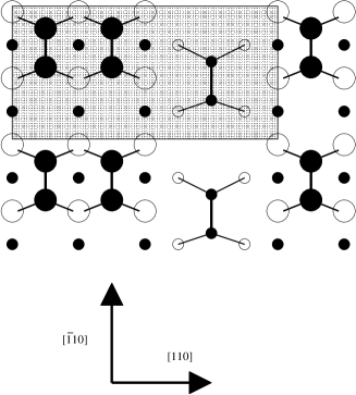
If this growth mechanism is true, a quite large portion of a GaAs(001) surface must reduce the widths of the trenches from double to single before islands nucleate. However, no scanning tunneling microscope (STM) images obtained thus far seem to support it.
Here we carry out atomic-scale Monte Carlo (MC) simulations as the alternative means to investigate nucleation and growth of islands on the GaAs(001)- surface. For this purpose, we developed the two-species model of homoepitaxial growth on the GaAs(001)- structure [3].

For the arsenic deposition process, we use As2 molecules, for which we simplify the incorporation process onto a surface structure in a mean field manner by introducing the chemical reservoir, where deposited As2 molecules are once stored. This process is schematically drawn in Figs.2 (a) and (b), where R, S, and V denote, respectively, the reservoir state, the surface-incorporated state, and the vacuum, which is far distant from a surface.
As Figs.2 (a) and (b) indicate, whether an As2 molecule can be incorporated onto a surface site depends on if surface Ga atoms are properly arranged there or not. When they are properly arranged, the incorporation channel of an As2 molecules becomes open, and the potential for As2 molecules changes from Fig.2(a) to Fig.2(b). As a consequence, the macroscopic growth rate is controlled by the deposition rate of Ga atoms. However, at atomic scales, arsenic species come into play in the growth kinetics, as we will see below. Note that this treatment of the chemisorption process improves the efficiency of computation, so that we can study the morphology of a growing surface in a realistic computation time.

For the interactions between surface atoms, we take account of those between the same species in the same layers, as depicted for the Ga-Ga interactions in Fig.3 and for the As-As interactions in Fig.4.
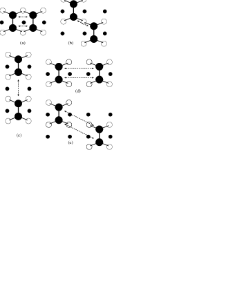
Among them, the interactions in Figs.4 (d) and (e), representing the Coulomb repulsions between two surface As atoms, play the central role in realizing the structure [4]. We note that these interaction parameters were determined solely by the comparison between the calculation results and the STM images.
By carrying out simulations with the kinetic MC algorithm [5], we found that the nucleation of islands take place on top of the substrate without having the structure, which transform into the structure at a later stage of growth [3]. This is because the excess charge on surface As atoms, which is the origin of the Coulomb repulsions in Figs.4(d) and (e), is not significant on small islands. The processes of nucleation and the structural transformation are well exemplified by the series of the snapshots in Fig.5.

To further confirm the validity of our model quantitatively, we plotted in Fig.6 the island-size distributions obtained by carrying out the calculations on the lattice as well as on the lattice and compared them with the STM images obtained at several different coverages. Here the lattice spacing in the model calculations corresponds to 4.0Å on a real surface. The result of the comparison for the total number of islands is displayed in Fig.6.

In this comparison, the results of the calculations were obtained at C, whereas the STM images were obtained after quenching the surface down to room temperature. In order to avoid the ambiguity caused by this difference in the conditions, we examined the effect of quenching, i.e., we performed the quenching simulations to find that single As dimers appearing at C change into double ones by quenching, so that the number of islands does not change during this process. We further found that other transient non- structures tend to adopt the structure during quenching. These results indicate that we can avoid the ambiguity and, hence, we can carry out a reliable comparison between the simulations and the STM images if we count the numbers of islands before, during, and after the splitting separately by classifying them into unsplit, partially split, and split islands, and discard the partially split ones, because they appear only as transient non- structures. The results are seen in Fig.7 to show a very good agreement between them.
Since Ga atoms prefer to reside at trench sites, As2 molecules can stick onto them and the width of the trench does change locally from double to single, as suggested by the ab initio calculations [2]. However, according to our calculations, these surface As dimers desorb from such sites within 1 ms at C, so that actually these processes do not result in the growth of islands. Instead, when Ga atoms gather on top of the As-dimer row of the structure and an As2 dimer sticks onto them, this is stable enough to be the nucleation site. Note that the complexity of this process is the origin of the significant delay in the nucleation time seen in Figs.6 and 7.
Our results show that the nucleation of an island is controlled by Ga kinetics, whereas the structural transformation and, accordingly, the appearance of the structure on newly created islands is due to the splitting process seen in Figs. 5 (d–l), which are controlled principally by the Coulomb repulsions in Figs. 4 (d) and (e), and thus, by As kinetics. By further employing the rate equations, we confirmed that these two are the only rate-limiting processes at the pre-coalescence regime of GaAs(001) homoepitaxy [6].

In summary, by carrying out atomic-scale growth simulations of GaAs(001)- structure, we found that the nucleation of islands takes place on top of the substrate and the islands grow via the structural transformation from non- structure to the structure. We further showed the validity of our model study quantitatively by comparing the results with those obtained by scanning tunneling microscopy observation.
Acknowledgements
One of the authors (M.I.) would like to thank Dr. T. Ohno for his encouragement.
References
- [1] M. J. Kelly, Low-Dimensional Semiconductors, Clarendon Press, Oxford (1995).
- [2] P. Kratzer, C. G. Morgan, and M. Scheffler, Phys. Rev. B 59, 15246 (1999).
- [3] M. Itoh, G. R. Bell, A. R. Avery, T. S. Jones, B. A. Joyce, and D. D. Vvedensky, Phys. Rev. Lett. 81, 633 (1998).
- [4] J. E. Northrup and S. Froyen, Phys. Rev. B 50, 2015 (1994).
- [5] A. B. Bortz, M. H. Kalos, and J. L. Lebowitz, J. Comp. Phys. 17, 10 (1975).
- [6] M. Itoh, G. R. Bell, B. A. Joyce, and D. D. Vvedensky, unpublished.