A millimeter-wave antireflection coating for cryogenic silicon lenses
Judy Lau, Joseph Fowler, Tobias Marriage, and Lyman Page
Princeton University
Department of Physics, Jadwin Hall
Princeton, NJ 08544, USA
Jon Leong
Case Western Reserve University
Department of Physics
Rockefeller Hall 10900 Euclid Avenue
Cleveland, OH 44106, USA
Edward Wishnow
Lawrence Livermore National Laboratory
7000 East Avenue
Livermore, CA 94551, USA
Ross Henry and Ed Wollack
NASA Goddard Space Flight Center
Observational Cosmology Laboratory
Greenbelt, MD 20771, USA
Mark Halpern, Danica Marsden, and Gaelen Marsden
University of British Columbia
Department of Physics and Astronomy
Vancouver, BC, Canada V6T-1Z1
Abstract
We have developed and tested an antireflection (AR) coating method for silicon lenses at cryogenic temperatures and millimeter wavelengths. Our particular application is a measurement of the cosmic microwave background. The coating consists of machined pieces of Cirlex glued to the silicon. The measured reflection from an AR coated flat piece is less than 1.5% at the design wavelength. The coating has been applied to flats and lenses and has survived multiple thermal cycles from 300 to 4 K. We present the manufacturing method, the material properties, the tests performed, and estimates of the loss that can be achieved in practical lenses.
1 Introduction
Silicon is a promising lens material for millimeter wavelength observations because it can be machined; it has a high index of refraction, which is optically advantageous; and it has a high thermal conductivity, allowing for straightforward cooling of the lenses to cryogenic temperatures. However, the high index () in the submillimeter region[1] leads to a reflection at each silicon/vacuum interface of approximately per surface. This is prohibitively large, especially for multi-lens cameras. Nevertheless, the benefits of silicon have motivated the development of antireflection coatings, [2, 3, 4, 5] where the referenced AR solutions are in IR and thus easier than mm-wave bands due to the thickness of the AR layer. This paper details the development and testing of a simple antireflection coating that reduces reflection to per lens at the design wavelength while maintaining transmission at 300 GHz.
At a fixed wavelength the ideal, normal-incidence antireflection coating for a substrate of index in vacuum has an index of refraction of and is thick. In our application, we are building lenses for the Atacama Cosmology Telescope (ACT) camera[6] at 145, 217, and 265 GHz to measure the fine scale anisotropy of the cosmic microwave background. In the following, we focus on the 150 GHz band, for which the ideal antireflection coating has m and index .
The coating is a machined piece of Cirlex® [8] polyimide glued to silicon with Stycast® 1266 epoxy [9] and Lord Ap-134 adhesion promoter[10]. For the curved lens surface, a piece of Cirlex approximately 1 cm thick is machined to the curved shape and then held in a Teflon gluing jig shaped to match the lens surface while the epoxy cures.
2 Material Properties and Construction Details
The low-frequency ( kHz) dielectric constant and loss reported in the Kapton polyimide data sheet[7] suggest that polyimide and silicon could be combined in an AR configuration. To ensure accurate modeling and to test sample dependent effects, we measured the dielectric properties with Fourier Transform Spectrometers (FTS), summarized in Table 1.
| Material | Relative dielectric constant 111The values are fit to transmission measurements in the frequency range GHz. Throughout, is in GHz.222All results are at ambient temperature. | 333Loss tangent is measured at 150 GHz. Results have relative uncertainty of 10%, or 15% on the thinner Cirlex sample. |
| Silicon () | ||
| Cirlex (0.25 mm) | 0.011 | |
| Cirlex (10 mm) | 0.008 | |
| Stycast 1266 | 0.023 |
Cirlex is a black pressure-formed laminate of Dupont Kapton® polyimide film readily available in sheets up to 597 mm 597 mm, and thicknesses from 0.2 mm to 3.175 mm, with thicker constructions possible. In the 100–400 GHz range, at room temperature, we find that the complex dielectric constant is well modeled as = with in GHz. At 150 GHz the loss tangent is given by:
| (1) |
To test the cryogenic properties of Cirlex, we placed a 250 m thick sample in a Bruker IFS 113 FTS that operates between 300 and 3000 GHz. Fitting a single complex dielectric constant across this frequency range, we measure () at 5 K, and () at room temperature. Note that when the temperature is reduced, the loss tangent decreases and the real part of the dielectric constant increases.
We also performed tests using a vector network analyzer to confirm the temperature-dependent behavior of Cirlex. Thin slabs ( 0.02 cm) of Cirlex were inserted into WR-10 waveguide and tested at 90 GHz both at room temperature and in a liquid nitrogen bath. The full complex scattering matrix was measured over the WR-10 band (75–110 GHz). The boundary conditions on the electric and magnetic field at both ends of the sample lead to expressions for the scattering parameters. The expressions depend on the length of the sample and its permeability and permittivity, and we invert them to derive the complex dielectric constant. [11, 12] At 77 K, Re () and at room temperature, Re (). Though we have not corrected for the dimensional change of the sample upon cooling ( shrinkage), it is clear that the loss decreases.
Our observations of Cirlex are consistent with a smooth increase in Re() from 100 GHz to 1 THz. In our calculations we use the value in Table 1, which corresponds to a best fit of the room-temperature data over the 90–300 GHz range. The loss is less well constrained, though it clearly decreases upon cooling. Table 1 shows that two similar samples exhibited losses differing by approximately 30%. Surface effects may be to blame, but we also note that the difference has low statistical significance.
Stycast 1266 is a two-component, low viscosity epoxy made by Emerson Cuming. We measured its properties with a cured sample machined to be flat and 0.64 cm thick. These properties are given in Table 1. The index of refraction is similar to that of Cirlex, but the loss is two to three times larger. To adhere the Cirlex to the silicon we coat the silicon with Lord Ap-134 adhesion promoter before applying the Stycast. The adhesion promoter is needed to ensure the coating can endure multiple cryogenic cycles.
We used high purity, high resistivity silicon for our lenses and test samples. Recall that the complex dielectric constant for a weakly conducting dielectric is
| (2) |
in the MKS system, where Re() is the real part of the dielectric constant, ( cm Hz)-1, and is the resistivity. For a -cm sample at 150 GHz, this corresponds to , close to the measured value. Prior studies of the loss in high-resistivity silicon show a complicated temperature dependence.[13] However, the loss is always smaller at 4 K than at room temperature for potential optical components.
Some care must be exercised when measuring the optical properties of silicon because both heating and ultraviolet light raise its conductivity. The nitrogen source used in the FTS was a critical improvement over the mercury arc lamp used initially. The arc lamp produced UV and heated the silicon samples to C or higher. We have observed both effects affect the resistivity of the silicon (and hence its optical transmission); heating to C alone reduced the resistivity by a factor of five.
In our experience, when a plastic sheet is glued to a glass, quartz or silicon substrate and cooled to liquid nitrogen temperatures, differential thermal contraction can shear apart the substrate. Silicon and Stycast 1266 thermally contract from 296 K to 4 K with and , respectively.[14, 15] We expect Cirlex to have a coefficient of thermal expansion comparable to that of a plastic, i.e. approximately that of Stycast 1266 and ten to one hundred times that of silicon. Through repeated testing, we have found that the composite structure does not fracture upon cooling if a thin layer of adhesion promoter is applied before the epoxy.
We experimented with multiple antireflection-coated samples to test their robustness, including five flats—four 100 mm in diameter and one over 200 mm in diameter—and three plano-convex lenses. Both the 100 mm and the 200 mm flats were dunked from room temperature into liquid nitrogen over fifty times without damage. The lenses have been cycled four times to less than 4 K in a dewar, also without damage.
3 Measurements and Modeling
We have measured both the reflection and transmission of the AR-coated samples. The reflectometer is quick and straightforward to use, though it is limited to only one frequency. The transmission measurements are necessary to understand the indices and the absorption losses, and they can be made at a wide range of frequencies.
3.A Reflection measurements
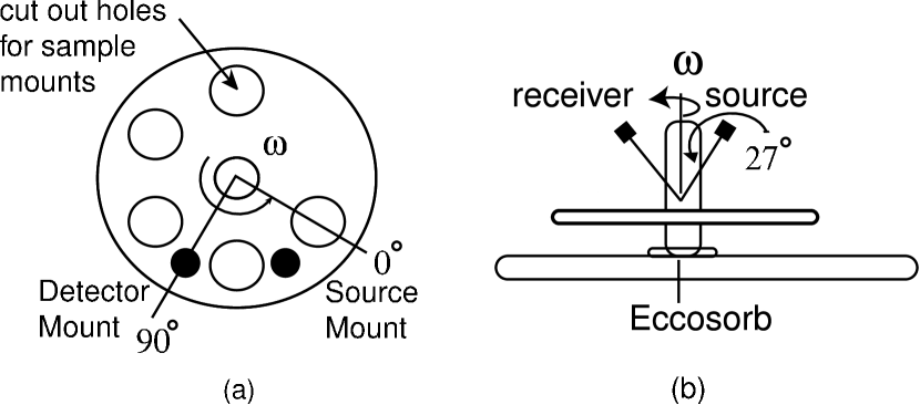
We built the reflectometer shown in Figure 1 in order to measure the reflection of the samples. Samples are mounted in 10.16 cm diameter holes on a 53.9 cm diameter, 1.23 cm thick rotating aluminum plate. Care is taken to ensure that the sample surface is in the same plane as the aluminum plate (m), and that the sample holder does not cause extraneous reflections. The diode detector, which measures total power, and a temperature-compensated 144.00 GHz source are mounted at a angle from normal incidence. The feed horns for the source and receiver are aligned so that the electric field is oriented normal to the plane of incidence (TE mode). As the disk rotates, the receiver successively views aluminum, a sample to be measured, or Eccosorb through an empty sample holder. The signal is synchronously binned and averaged over rotations of the plate. The data are then scaled by taking Eccosorb to have negligible reflection and aluminum to reflect perfectly.
To calibrate the reflectance , we placed silicon flats of known thicknesses (4–7 mm) into the reflectometer. The extremely narrow-band light source produces interference between reflections from the front and back of the silicon flats, so that varies between 5 and 70%, depending on the sample thickness. A single model of the reflection that incorporates the incident angle, polarization, sample thickness, frequency, and properties of silicon fits all the data with mean residuals. Figure 2 illustrates the ease of interpreting the raw reflectometer measurements. All lenses are measured with the flat side parallel to the aluminum plate.

Silicon flats and plano-convex silicon lenses were subsequently AR coated using the procedure detailed above. The reflection was measured before and after coating. The results shown in Table 2 demonstrate that both the flat and shaped silicon can be AR coated to achieve as little as reflection.
3.B Transmission measurements
Since we are primarily concerned with maximizing transmission through the lenses, the transmission spectra were also measured at room temperature on a FTS. The spectrometer uses the blackbody emission of Eccosorb foam submerged in liquid nitrogen as a light source. The detector is a composite bolometer with a Haller-Beeman NTD germanium thermistor and a mm nickel-chromium coated sapphire absorber. Liquid helium cools the bolometer to 4 K. Spectra were obtained between 100 and 425 GHz. The small aperture of the Winston cone feeding the bolometer sets the lower frequency limit, and a 15 cm-1 capacitive-inductive grid lowpass filter in the optical system sets the upper limit. The interferometer scans continuously from cm to cm optical path difference (OPD). Bolometer data are digitized at 40 samples per second by a 16-bit data acquisition board.[16] Acquiring each spectrum requires eight minutes. In analyzing the interferograms, we have discarded data outside cm OPD and apodized the rest using a window function with Hann-like taper and a half-maximum at cm optical path difference. The results are insensitive to the details of the window, the shape of which is a compromise between suppressing noise and not suppressing the real variations in the transmission spectra of thick dielectric samples.
The transmission model (like the reflection model used in the previous section) assumes that light consists of plane waves normally incident on infinite, planar samples. The formalism is the characteristic matrix of stratified dielectric media, given in §1.6 of Born and Wolf.[17] Unfortunately, the transmission cannot readily be expressed as a function of frequency for any system with two or more layers of dielectric. The light incident on the samples has a focal ratio of , slow enough that we can ignore wavefront curvature and polarization effects in the model. Two other effects must be considered, both of which tend to suppress in real FTS data the extremes of the idealized channel spectrum. First, it is necessary to treat the model as if it had been taken on the FTS by apodizing its “interferogram” with the same window applied to the data. More importantly, the model must sample the exact same frequencies as the measurements do, where the frequency step size is the inverse of twice the maximum optical path difference (in this measurement, the frequencies are spaced at 0.8 GHz). With these precautions, we find an excellent match between the measured and modeled transmission spectra of the coated (and uncoated) samples.
We were unable to measure the transmission of lenses directly. It was possible to obtain a spectrum of the transmitted light, but this spectrum included the confounding factor of the lens’s optical power. This optical gain factor can be computed in principle, but it requires detailed knowledge of the complete FTS optical system. Worse, it is not robust against small variations in the lens placement. For example, one sample’s spectrum differed by a factor of two between successive tests in which the lens was moved in the FTS beam by less than 5 mm. We find that the primary value of lens transmission measurements is to check for high transmission at the target frequency and at .
| Sample | Thickness444Center thickness is given for the plano-convex lenses. All lenses have edge thickness of mm. (mm) | uncoated | coated | Epoxy Thickness555This is the total epoxy thickness, not per side. (mm) |
|---|---|---|---|---|
| Flat 5 | 5.0 | 0.59 | 0.009 | |
| Flat 6 | 7.0 | 0.05 | 0.05666Due to the large epoxy layer, the coating was less successful. | |
| Flat 7 | 4.1 | 0.38 | 0.005 | |
| Lens 1 | 5.7 | 0.28 | 0.016 | |
| Lens 2 | 7.7 | 0.61 | 0.015 | |
| Lens 3 | 9.7 | 0.47 | 0.015 |
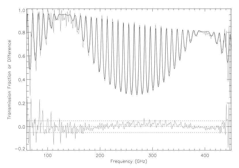
Rather than trying to interpret the lens results, we measured the transmission of the two coated flats labeled Flat 6 and 7 in Table 2. Figure 3 shows the transmission spectra for one of these samples along with a model. The measurement is the ratio of a sample to a reference spectrum, which are averages over two and six spectra, respectively. The model is not a fit to the coated transmission data but is determined instead by the Cirlex, Stycast, and silicon properties given in Table 1 and by measurements of the component thicknesses. The one exception is the silicon loss. The coated flats have somewhat lower resistivity (between 1300 and -cm, as measured by the vendor) than the uncoated silicon samples (all specified to exceed -cm); both sets have poorly constrained . To handle the uncertain silicon loss, we have treated the resistivity of the sample as an unknown and varied it to fit the measured transmission.
3.C Design Considerations
A finished design of a silicon antireflection coating for any application requires a complete model of the system. Incident angle range, frequency bandwidth, and polarization all affect the optimal coating thickness. It is helpful to begin the process with a few estimates and approximate guidelines, however, and we offer some here. First, using Equation 2 and recalling that power loss is one per radian of phase, we find that absorption loss in 10 k-cm silicon should equal 1% per centimeter, scaling as .
For normally incident light, the best AR-coating thickness can be estimated by requiring that the optical path through both materials (coating and glue) equal one-quarter wave. That is,
| (3) |
Comparing this rule against the calculated reflection, we find that it overestimates the optimal AR thickness by approximately m for a glue layer m thick. The difference increases quadratically with glue thickness, but the approximate expression is adequate for any reasonable size of the glue layer.

Figure 4 shows the predicted absorption and reflection loss calculated for a pair of realistic coated lenses, both at and incident angles. The model assumes lenses made of 5000 -cm silicon, 5 or 20 mm thick, and unpolarized light. Over most of the frequency range it should be possible to achieve better than 2% reflection per lens and less than 10% absorption particularly if the lens is thin or silicon resistivity is greater than the -cm assumed here.
It might be possible to use the Stycast 1266 alone as an AR coating. Its index of 1.68 is lower than the ideal 1.85, and the loss is approximately double the loss of Cirlex. However, cutting a single mold to shape the curing epoxy saves three machining steps when compared with the method for cutting Cirlex coatings described in this article. At 150 and 300 GHz, the optimal Stycast thickness are 300 and 140 m, which offer transmission of 90% and 88%, respectively. This compares unfavorably with the 95% and 93% transmission offered by a Cirlex-coated lens. The Stycast-coated lens would reflect approximately 1.5% in both frequencies, three times the reflection expected from a Cirlex-coated lens. Still, a simpler Stycast-only coating might suffice in some applications if the thickness and shape could be controlled well enough.
4 Conclusion
We have developed and tested a technique for antireflection coating silicon lenses at cryogenic temperatures at millimeter wavelengths. Flat samples show 1.5% reflection and 92% transmission at the design frequency. The remaining 6.5% is attributable to absorption loss, which will decrease upon cooling.
Acknowledgments
The authors are very grateful to John Ruhl for sharing his Fourier Transform Spectrometer and to Norm Jarosik for operating a Vector Network Analyzer. We thank the Princeton University Physics Department machine shop, especially Glenn Atkinson, for developing techniques to machine and glue the Cirlex coatings. Sarah Marriage tested different ways of gluing silicon to polyimide; Ted Gudmundsen and Adrian Liu repeatedly cycled coated silicon samples between 77 and 300 K. We are grateful to our colleagues on the ACT collaboration and to Asad Aboobaker, Andrew Bocarsly, Mark Devlin, Simon Dicker, Phil Farese, Jeff Klein, Jeff McMahon, Amber Miller, Mike Niemack, Suzanne Staggs, and Zachary Staniszewski for many helpful discussions. This work was supported by the U.S. National Science Foundation through awards AST-0408698 for the ACT project and PHY-0355328 for the Princeton Gravity Group.
References
- [1] J.W. Lamb, “Miscellaneous data on materials for millimeter and submillimeter optics,” Int. J. IR and Millimeter Waves 17, 1997–2034, (1996).
- [2] G.H. Sherman and P.D. Coleman, “Antireflection coatings for silicon in the 2.5-50 m region,” Appl. Opt. 12, 2675–2678 (1971).
- [3] S. Biber, J. Richter, S. Martius, and L.-P. Schmidt, “Design of Artificial Dielectrics for Anti-Reflection-Coatings,” in 33rd European Microwave Conference, Munich, 1115–1118 (2003)
- [4] N. G. Ugras, J. Zmuidzinas, and H. G. LeDuc, “Quasioptical SIS Mixer with a Silicon Lens for Submillimeter Astronomy,” in Proceedings of the 5th International Symposium Space Terahertz Technology, 125.
- [5] A. J. Gatesman, J. Waldman, M. Ji, C. Musante, and S. Yngvesson, “An Anti-Reflection Coating for Silicon Optics at Terahertz Frequencies,” IEEE Microwave and Guided Wave Letters, 10, 264–266.
- [6] J. W. Fowler, “The Atacama Cosmology Telescope project,” Proc. SPIE 5498, 1–10, (2004).
- [7] E.I. du Pont de Nemours and Company, 1007 Market Street, Wilmington, DE 19898.
- [8] Fralock, Division of Lockwood Industries, Inc., 21054 Osborne Street, Canoga Park, CA 91304.
- [9] Stycast 1266, Emerson and Cuming, 869 Washington Street, Canton, MA 02021.
- [10] Chemlok AP-134, Lord Corporation, 111 Lord Drive, P.O. Box 8012, Cary, NC 27512.
- [11] W. B. Weir, “Automatic measurement of complex dielectric constant and permeability at microwave frequencies,” Proc. IEEE, 62, 33–36, (1974).
- [12] J. Baker-Jarvis, E. J. Vanzura, & W. A. Kissick, “Improved technique for determining complex permittivity with the transmission/reflection method,” IEEE Trans. Microwave Theory Tech. 38, 1096–1103, (1990).
- [13] V.V. Parshin, R. Heidinger, B.A. Andreev, A.V. Gusev, and V.B. Shmagin, “Silicon as an advanced window material for high power gyrotrons,” Int. J. IR and Millimeter Waves, 16, 863–877, (1995).
- [14] T.H.K. Barron, & G. K. White, “Heat Capacity and Thermal Expansion at Low Temperatures,” (Kluwer Academic, New York, New York, 1999).
- [15] G.W. Swift and R.E. Packard, “Thermal contraction of Vespel SP–22 and Stycast 1266 from 300 K to 4 K,” Cryogenics 19, 362–363 (1979).
- [16] Diamond-MM-32-AT PC/104 board, Diamond Systems Corporation, 8430-D Central Avenue, Newark, CA 94560.
- [17] M. Born and E. Wolf, Principles of Optics, 7th Ed. (Cambridge, Cambridge, 1999).