Scientific performances of the XAA1.2 front-end chip for silicon microstrip detectors
Abstract
The XAA1.2 is a custom ASIC chip for silicon microstrip detectors adapted by Ideas for the SuperAGILE instrument on board the AGILE space mission. The chip is equipped with 128 input channels, each one containing a charge preamplifier, shaper, peak detector and stretcher. The most important features of the ASIC are the extended linearity, low noise and low power consumption. The XAA1.2 underwent extensive laboratory testing in order to study its commandability and functionality and evaluate its scientific performances. In this paper we describe the XAA1.2 features, report the laboratory measurements and discuss the results emphasizing the scientific performances in the context of the SuperAGILE front-end electronics.
keywords:
High Energy Astrophysics , X-rays , front-end electronics , ASIC , silicon microstrip detectorsPACS:
29.40.Wk , 85.40.Qx , 95.55.Ka, , , , , , , , , , , , , ,
1 Introduction
The new generation of tracking, vertex and pixel detectors for High Energy Physics experiments, as for example the ATLAS and CMS detectors at LHC, is based on silicon microstrip detectors. This type of sensors offers a high spatial resolution combined with a wide surface, a good signal-to-noise ratio and a fast response. Standard silicon strip detectors, now common in High Energy Physics experiments, can be successfully used for position-sensitive detection of X-rays. A similar type of detectors is suitable in many applications and experimental techniques in solid-state physics, material science and biological study using synchrotron radiation, as shown for example in [1].
Space Astrophysics is now starting to take advantage of the peculiar features of the silicon microstrip detectors, mainly the possibility of building large and light detectors with extremely high spatial resolution, as proposed in [2] and [3]. Particularly, replacing the gaseous detectors with solid-state detectors allows to increase the lifetime of the space missions, increase the spatial resolution up to m level for on-axis experiments and to tens of m in case of inclined penetration and reduce the deadtime from ms to s ([4]). The detectors of PAMELA ([5]), space experiment for Cosmic Ray Physics launched in spring 2006, AGILE ([6]) and GLAST ([7]), the next satellite-borne missions for High Energy Astrophysics in the X-ray and gamma-ray energy bands, are all based on the silicon microstrip technology.
The use of solid state detectors, in both Space and ground based experiments, allows to increase the number and density of independent channels number and density, thus requiring the ASIC technology in the integrated front-end electronics. Critical parameters for the front-end electronics of the silicon microstrip detectors, in both ground and space experiments, are noise, speed, power consumption and radiation tolerance. The noise introduced by the detector depends on the leakage current shot noise, bias resistors thermal noise, metal strips Johnson-type noise and statistic fluctuation of the charge carriers. Depending on the energy of the interacting particle, Equivalent Noise Charge values of the order of can be achieved. The bunch crossing time in High Energy Physics and the flux variability in Astrophysics experiments require a signal processing time of the order of 1 s. The amount of power available from solar panels in a satellite-borne experiment and the difficulties associated with supplying and cooling the electronics in an accelerator experiment require power consumption of the order of 0.1–1 mW per input channel. Finally, the levels of total ionizing dose, both in accelerators and in Space, require radiation tolerance in the krad–Mrad range. A more complete view of the requirements of the readout of silicon microstrip detectors and the architectural and technological options may be found in [1].
In this paper the functional and scientific performances of the XAA1.2, as the front-end electronics circuit of the SuperAGILE instrument, are reported. The structure of the paper is as follows: section 2 contains the overview of the SuperAGILE instrument and the AGILE mission, in section 3 the description of the XAA1.2 electronic circuit is reported, section 4 deals with the description of the experimental set-up, in section 5 we discuss the most important sources of noise in systems based on the silicon microstrip detectors, the results of the linearity and noise measurements with a test pulse and X-ray calibration sources are in section 6 and 7 respectively, the threshold measurements are in section 8, section 9 contains the outline of the electronic noise reduction method by means of the signal shape adjustment, the measurements of the thermal stability of the output signals are in section 10, in section 11 we give an outlook of the XAA1.2 radiation tolerance and finally section 12 contains the conclusions.
2 Overview of the SuperAGILE instrument and the AGILE mission
AGILE is a satellite-borne mission dedicated to the gamma ray and X-ray Astrophysics. The AGILE payload contains two instruments, the Gamma Ray Imaging detector (GRID) and the SuperAGILE X-ray monitor, both equipped with silicon microstrip detectors. The GRID ([8]) is sensitive between 30 MeV and 50 GeV and is composed of a Silicon Tracker, with tungsten converters and silicon microstrip detectors, complemented by a Mini-Calorimeter with CsI(Tl) scintillator bars ([9]). SuperAGILE ([10]), the AGILE X-ray monitor, is a coded aperture instrument equipped with silicon microstrip detectors and tungsten coded mask and is sensitive to hard X-rays in the 15–45 keV energy band. SuperAGILE is located in the field of view of the GRID and the two instruments are designed as a single experiment. The payload is surrounded by a plastic scintillator Anticoincidence shield ([11]). AGILE is an ASI (Agenzia Spaziale Italiana) satellite mission and its launch is planned on 2007. The satellite will be positioned on an equatorial orbit with about 560 km altitude. Further details about the AGILE mission and scientific objectives may be found in [6]. An overall description of the SuperAGILE experiment will be reported in a forthcoming paper [12]).
Among the scientific objectives of the AGILE mission are the Gamma Ray Bursts (about 15–20 events per year are expected in the hard X-ray band and 5–10 events per year in the gamma ray band, they will be localized on board and their coordinates will be distributed to the scientific community by means of the ORBCOMM111Web site: www.orbcomm.com satellite constellation), Active Galactic Nuclei (with study of transients and low-level gamma ray emission and duty cycles, observation of the relationship and correlation between the gamma ray variability and the radio, optical, X-ray and ultra high-energy emission), Compact Galactic Sources (Gamma Ray Pulsars, Unidentified EGRET sources, black hole candidates, X-ray binary systems and Soft Gamma-Ray Repeaters outbursts) and Diffuse Emission (with the study of cosmic ray origin, propagation, interaction and emission processes).
SuperAGILE can produce images of the sources in the Sky using the coded aperture imaging principle, based on a position sensitive detector coupled to a plane with a pattern of pixels opaque and transparent to the radiation under study and distributed following a specific code (“coded mask”). The X-ray sources cast unique shadows of the mask on the detector and the photons direction can be reconstructed using proper algorithms. More details about the coded mask instruments, their principle and their performances as imagers for High Energy Astrophysics may be found in [13] and [14].
The SuperAGILE detector is composed of four modules of one dimension silicon microstrip detector tiles (manufactured by Hamamatsu) of cm2 area and 410 m thickness, each one containing 1536 strips. Each detector module is composed of two ladders with 768 strips and surface, composed in turn of two square tiles of 9.5 cm side, bonded head-to-head with consecutive strips. The detector capacitance is 30 , the pitch of the microstrips is 121 m and above each strip an aluminum electrode (of 72 resistance) is positioned, separately connected to an input chain of the XAA1.2. The detector is biased at about V on the back side. The detector modules are glued on a honeycomb and carbon fiber tray.
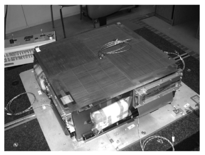
At 14.1 cm above the detector the coded mask is fixed, manufactured on a single tungsten plate 120 m thick, glued on a carbon fiber layer 500 m thick. The mask plate is subdivided into four one dimension modules, each one of the same surface as the detector module below and with 787 pixels of 19 cm length and 242 m width. The mask-detector geometry gives a resulting pixel size of 6 arcmin. For intense sources the location accuracy can be improved as the inverse of the signal to noise ration (S/N), down to a systematics expected of about 1 arcmin. The coded mask is supported by a tungsten (100 m) and carbon fiber (500 m) collimator, that defines also the instrument field of view as two orthogonal . A picture of the SuperAGILE flight model is shown in fig. 2.
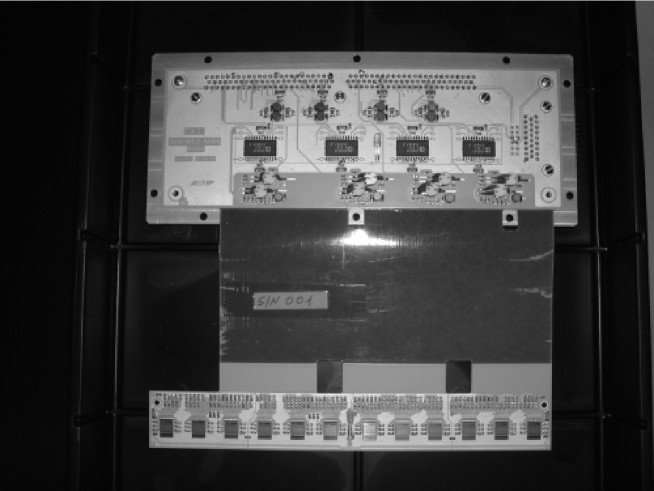
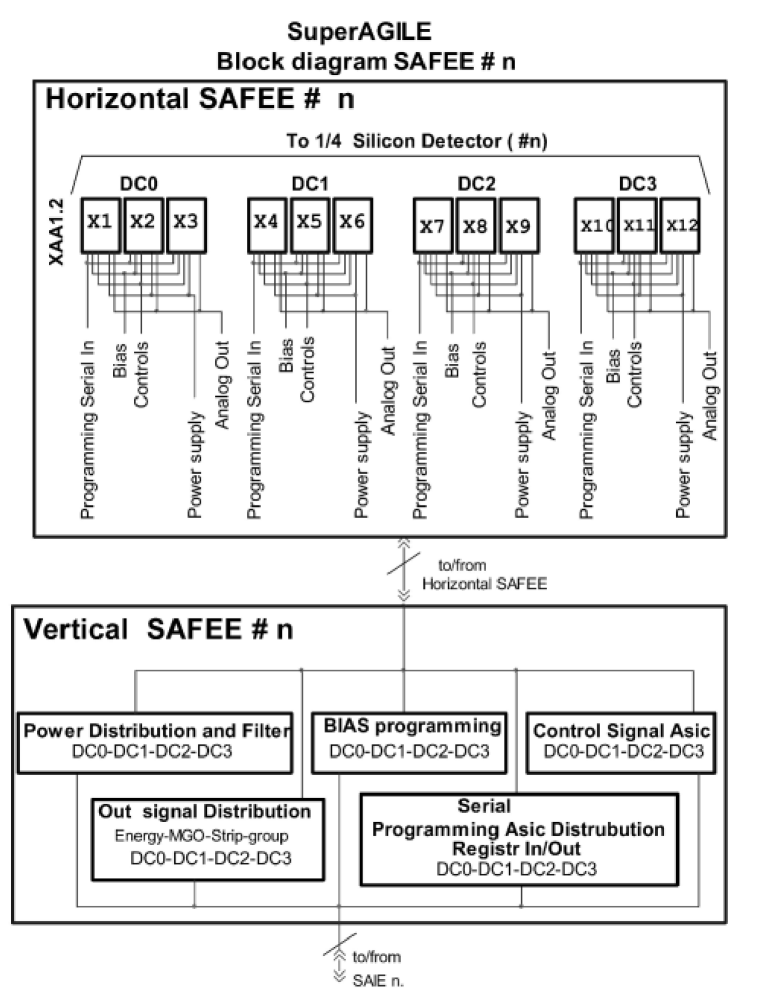
The SuperAGILE front-end electronics (SAFEE) is composed of four Rigid-Flex Printed Circuit Boards (PCB), each one containing twelve chips XAA1.2 and interfaced to a detector module using pitch adapters. In the SAFEE layout the XAA1.2 are arranged in four daisy chains of three chips each and a daisy chain is considered as a single and independent unit with its input and output connections. The power supply, biases (voltages and currents) and output bus are common in a single daisy chain. The biases and reference voltage to a single daisy chain are generated using an octal Digital to Analogue Converter (DAC) chip, AD8842AR unit. Because of the small room on the SuperAGILE tray, the SAFEE board is divided in two sections: the horizontal SAFEE, lying on the the detection plane and containing the XAA1.2 chips, and the vertical SAFEE, containing the DAC units and all the other conditioning electronics (power supply distribution, filters, bias generation, serial programming and output buffers) and fixed on the collimator external wall. A picture of the SAFEE PCB before the integration to the detector is shown in fig. 2. Two AD590KF temperature sensors are mounted on the SAFEE PCB, one in the horizontal board and the other in the vertical board. A block diagram of the SAFEE electronics is shown in fig. 3.
3 Description of the XAA1.2 chip
The XAA1.2 is an application specific integrated circuit (ASIC) designed by means of the very large scale integration (VLSI) technology by Ideas ASA (now Gamma Medica-Ideas222Web site: www.gammamedica.com) as a front-end electronic chip for silicon microstrip detectors. The chip is manufactured with a 0.8 m complementary metal oxide semiconductor (CMOS) double-poly and double metal technology (corresponding to a 16 nm gate-oxide thickness) on epitaxial layer. A block diagram of the XAA1.2, showing the analog and digital sections of the circuit, can be seen in fig. 4. The XAA1.2 has been partially optimized as front-end electronics of the SuperAGILE instrument. In particular, the input FETs were modified in order to match the 30 load of the SuperAGILE detectors and the power consumption lowered of a factor 3–6.
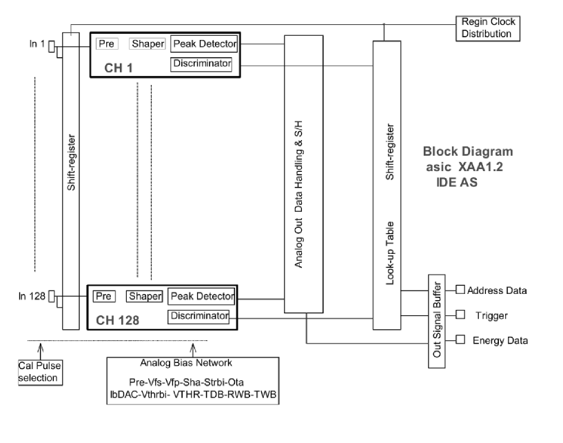
The XAA1.2 surface is and its thickness is 600 m. The circuit is divided into 128 data driven and self-triggering input channels, consisting of an analogue and a digital section, and is designed to detect single hit events with sparse readout. Each analogue signal processing chain is in turn composed of a charge sensitive preamplifier, a CR-RC shaper and a peak sensitive stretcher, as sketched in fig. 4. The peak stretcher can be excluded from the analogue processing of one circuit by changing the digital configuration of the ASIC, thus reducing the overall power consumption. The analogue chains are followed by a Analogue Out Data Handling and Sample and Hold (S/H) stage. The main features of the XAA1.2 as a front-end electronic circuit for silicon microstrip detectors were reported in [15]. The XAA1.2 is a custom ASIC chip designed starting from the commercial device XA1.3 aiming to improve the performance in terms of noise, power consumption and thermal stability after the extensive laboratory testing reported in [16].
The XAA1.2 digital section can be programmed by serially loading an internal 646-bit register. The register content (referred to as configuration mask or “Register In”) encodes all the information needed to configure the chip: 128 bit specifying the enabled channels in test mode (for an electrical stimulus to be injected as described in section 6), 384 bit configuring the threshold fine regulation (3 bit per channel), 128 bit specifying the disabled channels, 4 bit containing the address offset (to address up to sixteen XAA1.2 connected in daisy chain), 1 bit enabling the stretcher and 1 bit enabling the chip in test mode. By sending twice the configuration mask the actual value contained in the memory (referred to as “Register Out”) is provided and can be read out.
The XAA1.2 is supplied using four highly regulated voltages, two for the analogue section ( and ) and two for the digital section ( and ). The power consumption of the digital part is negligible if compared with the analogue section. The measured supply currents of the chip in nominal bias conditions (shown in tab. 1) and stretcher-on configuration are and , thus giving an overall power consumption of about 1 .
The XAA1.2 functionality and performance are controlled by eleven biases and a reference voltage, all provided to the chip using external DAC units. The bias currents are prebias and shabias (controlling the source and the drain current of the preamplifier and shaper respectively), otabias (bias current of the discriminator), IbDAC (controlling the voltage to current buffer converters), strbias (bias current of the peak stretcher), Vthrbi (controlling the digital fine regulation of the threshold), TrigDelbias (setting the delay between the trigger and the internal sample and hold), TrigWbias (defining the hold width) and finally the ResWbias (affecting the width of the reset signal after an event is detected and processed). The bias voltages are Vfs and Vfp (DC voltages for the gate of the feedback MOS resistor in the preamplifier and the shaper respectively) and the reference voltage is Vthr. The default value of the bias currents and voltages are shown in tab. 1.
| Bias name | bias value |
|---|---|
| prebias | 80 A |
| shabias | 9 A |
| otabias | 10 A |
| strbias | 60 A |
| Vthrbi | 20 A |
| IbDAC | 60 A |
| TrigDelbias | 2 A |
| TrigWbias | 0.2 A |
| ResWbias | 0.1 A |
| Vfp | -125 mV |
| Vfs | 960 mV |
The XAA1.2 is developed as a front-end electronics chip for position sensitive silicon microstrip detectors. Following the internal chip logic the 128 channels are divided into four groups of 32 channels each. For this reason a single channel is identified by its position within the group (strip signal, 5 bit) and of its group within the chip (group signal, 2 bit). To the latter signal 4 offset bit can be externally added, encoded in the Register-In, to allow the identification of the chip in a daisy chain (of 16 XAA1.2 maximum). Since the internal chip logic is not able to provide information on more than one hit at a time, the switch of a threshold inhibits all the other inputs within a few nanoseconds range. If more than one event is present during this time interval, a multiple event is detected and its output signals are meaningless. The multiplicity of the processed events is provided by a multiplicity generator output (MGO signal), thus allowing to reject multiple hit events. Internal DAC units convert the strip, group and MGO signals into analogue current differential outputs, in order to reduce the pick-up noise. Consequently on trigger the XAA1.2 returns four pairs of differential output current signals: amplitude, strip, group and MGO.
The amplitude output signal from the ASIC shaper is affected by dumped oscillations, lasting for about 30 s. This “wiggle” is a constitutional property of the XAA1.2, due to a non perfectly matched mirroring of the currents inside the chip (B. Sundal, private communication), and cannot be fixed from the exterior. The “wiggle” does not allow to sample the signal before 20 s from the trigger and is a lower limit to the XAA1.2 dead time.
The analogue chains of the XAA1.2 can process charge pulses produced by an external generator, that is used to calibrate the electronics by replicating the output pulses from a detector. For this purpose the chip contains a test charge input where voltage pulses can be provided. Such voltage signals are then converted into charge by an internal 0.5 pF capacitor.
The threshold is set to the XAA1.2 using an external reference voltage, thus giving the same reference value for all the input channels. Moreover the XAA1.2 channels allow a 3-bit fine regulation of the analogue threshold, encoded in the configuration mask, to reduce the threshold intrinsic disuniformity.
4 Experimental set-up
The measurements reported in this paper have been performed with the XAA1.2 as part of the SAFEE circuit. For testing purposes, the SAFEE PCB is connected to a dedicated test equipment, based on VME bus with VME-PCI bridge and working under Linux operating system. The test equipment provides the power supply, programs the XAA1.2 internal registers, generates the voltage pulse to feed the test charge input, converts the output current signals to voltage, performs the analogue to digital conversion using a 12-bit Analogue to Digital Converter (ADC) and adds the time tag to the events. Particular care was devoted to the control and reduction of the electronic noise when designing, building and operating the test equipment. A detailed description may be found in [17]. Further details about the experimental set-up are given in the sections dedicated to the measurements.
5 Analytic estimation of the XAA1.2 noise contributions
The main sources of noise in ASIC circuits coupled to silicon microstrip detectors are the shot noise given by the leakage current in the detector, the thermal noise from the detector bias resistors, the noise produced by the metal strips and the transistor channel noise in the readout chip. All the other noise components in the input transistor, such as the flicker noise and the bulk-series resistance noise, are negligible when compared to the contributions listed above. In our set-up the channel noise is by far dominant over the other contributions. In this section an overview on the main sources of noise is given and each contribution is specialized to the case of the XAA1.2 chip, following the method in [18] applied to the silicon microstrip detector described in sec. 2.
The noise figures are generally expressed using the Equivalent Noise Charge (), a parameter connecting the root mean squared () noise voltage at the output of the shaper with the signal input and generally measured in . All the noise sources increase the width of a monochromatic energy input following a gaussian distribution. For this reason, the (in ) can be converted into the Full Width at Half Maximum () of a spectral line (in keV) taking into account the equation connecting the and the signal :
| (1) |
In case of the XAA1.2 chip, the shot noise given by the leakage current in the detector can be written as
| (2) |
where is the strip leakage current (in ), is the peaking time (in s) and is the temperature (in K). Considering that at room temperature (300 K) the SuperAGILE detector leakage current is and the signal peaking time is s, the contribution is and keV.
The thermal noise in the detector bias resistors can be written as
| (3) |
with . Substituting the numeric values applicable for SuperAGILE the estimated noise is and keV.
The ENC contribution of the detector metal strips is
| (4) |
and since for the SuperAGILE silicon microstrip detector and , and keV.
The XAA1.2 transistor channel noise is in principle given by
| (5) |
where is the flicker noise contribution, is the transistor channel component and is the transistor bulk-resistance noise. As shown in [18], the contributions from flicker and bulk resistance noise can be neglected and the transistor channel noise at the prebias nominal value of can be written with the semiempirical formula
| (6) |
composed of a contribution proportional to the input capacitance and a constant term taking into account the internal capacitance. The parameters in the (6) have been estimated from the laboratory measurements with the test pulse generator and include the Johnson noise contribution. Taking into account the capacitance of the detector ( ) the resulting noise is and keV.
Considering the mean energy needed to create a hole-electron pair in silicon ( eV), the fluctuation on the number of charge carriers produced by the interacting photon is one of the noise contributions introduced by the detector. Taking into account that the number of electron-hole pairs in the detector follows the Poisson statistics (corrected by the Fano factor) and that only the holes are processed by the XAA1.2, the contribution is
| (7) |
where is the number of detected holes and is the Fano factor of the material. Since in silicon (as reported for example in [19]), typical values of the detector noise contribution are (corresponding to keV) at 10 keV, (corresponding to keV) at 50 keV and (corresponding to keV) at 100 keV.
The total noise in the XAA1.2 chip is given by the combination of the contributions discussed above,
| (8) |
and it is found in this section that the transistor channel noise is by far the most important noise source. For SuperAGILE detector and front-end electronics the resulting from the (8) is and keV.
6 Measurement of the XAA1.2 linearity and noise using the charge test pulse generator
The linearity of all the XAA1.2 input channels can be measured using the test pulse generator (described in sec. 3). For each channel the mean value of the digitized output amplitude as a function of the input charge represents a measure of the linearity (referred to as “calibration curve”). Applying a linear fit to the calibration curve, the linearity parameters of the channels are separately evaluated in terms of offset (intercept of the linear fit) and gain (angular coefficient of the linear fit). A sequential measure of the linearity on all the XAA1.2 input channels with the test pulse generator is referred to as “electronic calibration”. All the measurements reported in this section deal with the XAA1.2 connected to the silicon microstrip detector through wire bondings.
In the electronic calibration the XAA1.2 is typically fed with input charges ranging from 0.5 fC (corresponding to about 11 keV in silicon) up to 5 fC (corresponding to about 113 keV in silicon). From these measurements we find that the XAA1.2 is linear up to 5 fC, the average residual of the linear fit being at this input charge value. An example of the distribution of the gain values of the 384 channels in a daisy chain is plotted in fig. 6. In the upper panel the histogram of the gain values is plotted while in the lower panel the gain value of each input channel is plotted. The vertical dotted lines in the lower panel separate the three chips within the daisy chain. The represented data are typical of the XAA1.2 chips, showing their level of disuniformity and difference.


The XAA1.2 noise is evaluated in each input channel as the mean value of the FWHM of the output amplitude histogram for the different input charges. The FWHM value, initially measured in ADC channels, is then converted into energy units by dividing it by the gain, obtained from the linearity fit. An example of the distribution of the FWHM noise values of the same 384 channels (as in fig. 6) is plotted in fig. 6. In the figure the upper panel shows the noise FWHM values histogram while the lower panel shows the noise FWHM values for each input channel. The vertical dotted lines in the lower panel separate the three chips within the daisy chain. The noise FWHM averaged over the 384 input channels is 7.5 keV with a 0.2 keV standard deviation. Again, the data reported here for three chips are representative of the general XAA1.2 behaviour. The measured FWHM is smaller than the theoretical estimations in sec. 5 because the noise has been reduced adjusting the amplitude signal shape following the method described in sec. 9.
7 Measurement of the XAA1.2 linearity and noise using the X-ray sources
A verification of the XAA1.2 linearity and noise has been performed by the acquisition of photons from calibration radioactive X-ray sources. The sources used in these measurements are (Ag K line at 22.1 keV), (decay line at 59.5 keV), (decay line at 122.1 keV) and a custom source emitting Ba fluorescence photons at 32.1 keV from a crystal excited by two sources.
The measurement statistics does not allow to fit the spectrum acquired by a single strip, so the spectra have been accumulated on a daisy chain. Since each microstrip can be considered as an independent detector, with its own gain parameters, a correction algorithm need to be applied to the data in order to accumulate the spectra. For this reason, the digitized amplitude (in ADC channels) of each detected photon has been converted into a conventional amplitude (in PHA) using the gain parameters of the triggered input channel, evaluated with the test charge measurements as in sec. 6 under the assumption that the test capacitor has the same value in each chip.
As an example, in fig. 8, 8, 10 and 10 the spectra acquired with the (22.1 keV line), custom (32.1 keV line), (59.5 keV line) and (122.1 keV line) are plotted. In order to obtain a significant statistics, the spectra of each source are accumulated on 383 input channels from the same subset as in sec. 6, apart from the last channel that is excluded from the acquisition since its noise contribution is much higher than the other channels because of a lower threshold.
The spectra in the figures from 8 to 10 are fitted with a model based on a gaussian function representing the X-ray line and a polynomial background depending on the specific source. In case of the and sources, where two lines are present that are not completely resolved because of the system spectral resolution, the fitting function includes both the lines, modeled using gaussians. The peak position of the gaussian from the fit is then linearly fitted as a function of the X-ray line energy
| (9) |
as shown in fig. 12. The parameters of the linear fit in (9) applied to the data sample in fig. 12 are PHA and and the linear fit is shown as a dotted line in fig. 12.


The parameter of the linear fit in (9) allows to correlate the linearity measurements performed with the electronic test pulse and with the X-ray sources, since the amplitude of the acquired photons is corrected on the basis of the calibration curve of the triggering channel. The variation of the fitted parameter with respect to the expected value of one is a measure of the systematic error of the correction procedure and is due to the variation of the input capacitance, that generates the input test pulse, with respect to the nominal 0.5 pF value. For this reason, the linear fit in (9) can be used to calibrate the test charge generator by correcting the input charge values in the calibration curve by the factor.
The noise in the spectrum is estimated from the gaussian standard deviation of the spectral fit, converted into the line following
| (10) |
where is the conversion factor between amplitude (PHA) and energy (keV) units as estimated in (9). The FWHM values of the data sample, estimated from (10), are plotted as a function of energy in fig. 12. As can be seen in the plot, FWHM from 7.1 keV (at 22.1 keV) up to 8.3 keV (at 122.1 keV) are found and the values are compatible at with the FWHM measured in sec. 6 using the test pulse generator.
8 Measurement of the XAA1.2 threshold
In the SAFEE architecture the same reference voltage Vthr is set to the discriminator of all the input channels in a daisy chain using the external DAC (AD8842AR). During the measurements the issue of converting the reference voltage into charge (and then into energy) is raised. In order to have the same operational threshold definition for both on-ground and in-orbit conditions, where the noise is different, the SuperAGILE threshold is defined starting from the background counting rate.
As a first step, background acquisitions are performed at high reference voltage, where the counting rate is dominated by the environmental background and the electronic noise contribution can be neglected. This measurement provides an estimate of the local environmental background, that depends on the site and will not be present in orbit. In orbit we expect two major components for the background counting rate: the Diffuse X-ray Background (DXB, see [20] for further information) impinging on the detector through the open slits of the mask and within the collimator aperture and the tail of the electronic noise, since the particle background is very efficiently eliminated by the upper threshold of the SAIE. Our current operational definition of threshold is such that the background counting rate is due to the DXB plus a 10 % due to electronic noise.
The threshold voltage estimated with the method outlined above is then converted into a charge threshold (and then into the corresponding energy threshold) by means of the threshold scan procedure. The threshold scan consists in feeding each input channel of the XAA1.2 with a fixed number of pulses at increasing reference voltage. With a proper setting of parameters, the counts detected for each value of the reference voltage will vary from the total number of pulses (at low threshold) to zero (at high threshold). Using a linear interpolation, the reference voltage is found such that the number of detected triggers equals one half of the number of input pulses. By repeating this procedure at different input charge values, the reference voltage value as a function of the input charge can be found, that is the characteristic curve of the discriminator of each channel of the XAA1.2. This relation can be used to convert reference voltage values to charge values and to energy, considering the 3.62 average energy to produce an electron-hole pair in silicon. Thus the voltage threshold, based on the background counting rate, can be converted into an energy threshold using the threshold-energy relation. The SuperAGILE threshold defined with this method is arbitrary and is mainly useful to compare conditions where the environmental background is different.
As an example, the histogram of the energy threshold of the same subset of input channels as in sec. 6 and 7 and measured using the method described above is shown in fig. 13. As it appears from fig. 13, the intrinsic threshold of the XAA1.2 channels is largely non uniform, with a typical standard deviation of 3.3 keV. A fine threshold adjustment is available, based on a 3-bit internal DAC, allowing to reduce the threshold spread. Unfortunately, the variation of the fine threshold of one channel affects all the other channels in the same daisy chain, introducing an offset to their threshold. For this reason, the fine threshold adjustment is an iterative procedure, starting with the threshold estimation of each channel with the method described above. The threshold is then reduced if it is higher and increased if it is lower than the mean value by changing the digital regulation in the XAA1.2 configuration mask according to a complex algorithm and the threshold scan is repeated in the new configuration. Usually in 2–3 steps the threshold spread is minimized.

From preliminary measurements, performed on a sample of 384 channels (connected to the silicon microstrip detector) with average threshold value about 20 keV, the fine threshold adjustment reduces the threshold spread by about a factor of two. A detailed description of the method and results on the SuperAGILE Flight Unit will be published elsewhere ([21]).
9 Optimization of the XAA1.2 performances by means of the signal shape adjustment
The transistor channel noise in the XAA1.2 can be reduced by increasing the transconductance through an increase of the prebias, controlling the source and the drain current of the preamplifier. Such a prebias variation produces also a reduction in the peaking time, affecting the shot noise, the thermal noise in the bias resistors and the noise due to the metal strips, all depending on the peaking time as reported in sec. 5. For SuperAGILE the prebias value is constrained by the chip power consumption, strongly affected by this bias. In order to keep the peaking time at the 2 s nominal value also the shabias, the Vfp and the Vfs have to be adjusted.
As an example, by increasing the prebias from 50 A to 85 A and adjusting correspondingly the shabias, Vfp and Vfs, the electronic noise of the XAA1.2 decreases from about 1070 , corresponding to 9.1 keV FWHM, to about 820 , corresponding to 7.0 keV FWHM with a power consumption increase of about 20–30 %.
The optimization of the signal to noise ratio can be performed as an iterative procedure involving the two bias currents prebias and shabias and the two voltages Vfp and Vfs, all affecting the signal shape. Since the XAA1.2 chip does not allow to access the analogue output signal from the shaper before the signal is processed by the peak stretcher and S/H, an indirect way to detect the shaper output signal (in order to control the effect of the bias currents and voltages variation on the signal shape) is to switch off the stretcher and to acquire signals at different TrigDelbias values, i.e. with different values of the delay between the trigger and the sampling time of the internal S/H, so reconstructing an oscilloscope-like signal shape image, as shown in fig. 15.

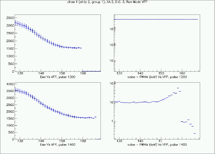
At the beginning of the optimization procedure the prebias is increased. A suitable value for SuperAGILE is about 80–100 A, compatible with its power budget. The value of the Vfp is then adjusted to about 100 mV above the value that produces the preamplifier saturation and the exact bias value is selected searching the minimum of the noise as a function of Vfp by using the test pulse generator, see for example fig. 15. The shabias and Vfs are then adjusted to keep the peaking time as close as possible to the 2 s nominal value and to reduce the noise. In this way the minimum of the noise can be found and the optimal values of the parameters can be selected.
10 Temperature dependence of XAA1.2 performances
The SuperAGILE instrument in orbit will work between and (operative temperature range). To characterise the temperature dependence of the XAA1.2 performances, we measured the variation with temperature of the gain (used to reconstruct the amplitude of the detected photons) and the address signals (needed to reconstruct the photons position).
The measurements were performed in a thermo-vacuum chamber, from to at 50 mbar pressure, using the electronic calibration procedure. The SAFEE PCB is glued to a carbon fiber and aluminum honeycomb tray, the SuperAGILE collimator and coded mask (carbon fiber and tungsten) are positioned above the PCB in order to keep the experimental set-up as close as possible to the true in-orbit conditions. Without the coded mask and collimator, in vacuum the temperature of the XAA1.2 (measured with an infrared thermometer) is about higher than the environment temperature, because of its power dissipation. The SuperAGILE temperature is monitored using 32 AD590KF thermometers and each SAFEE unit contains two thermometers, one placed in the horizontal board and the other in the vertical section. During the test the temperature has been measured with the thermometer located in the horizontal SAFEE board, the nearest one to the XAA1.2.
The gain mean value as a function of temperature between and are shown in fig. 16. Below the noise introduced by the thermo-vacuum chamber strongly affects the amplitude output signals and does not allow to perform the electronic calibration procedure. As shown in fig. 16, the XAA1.2 gain decreases as a function of temperature and the percentage variation is with a linear fit superimposed on the plot as a dotted line.

The superposition of the group digitized signals in the range between and is shown in fig. 17. As can be seen in the plot, the group signal shift depends on the temperature, being about 5 above and about 10 below . The average separation between two groups is 200 ADC ch. A temperature variation of about produces the superposition of the group signal in two consecutive groups of channels (for example the superposition between the first group at and the second group at ), that can cause an incorrect reconstruction of the triggering channel.

A similar shift as a function of temperature can be seen in the strip signal. A plot of the strip digitized signal of the first group (first 32 channels) is shown in fig. 19. For sake of clarity, a magnified view of the strip signal superposition is shown in fig. 19. As can be seen in the plot, the strip variation with temperature depends on the circuit channel under test, being negligible below channel 15 and important above channel 25. Particularly, between channel 15 and 25 a shift of one address channel is seen with a temperature variation of about while above channel 25 the same shift is produced by a temperature variation of .


11 Measurement of the XAA1.2 radiation damage
Since the XAA1.2 is not specifically designed as a radiation hard component for space applications, its radiation hardness required to be tested. Heavy ion irradiations were performed at the SIRAD irradiation facility of the Laboratori Nazionali INFN of Legnaro (see [22] for a complete description of the facility) to study the radiation damage of the XAA1.2, mainly latch-up, SEU and total dose effects.
The XAA1.2 mean LET threshold for the latch-up is with a mean limit cross section of cm2 and the LET threshold for the SEU is . The power consumption of the three XAA1.2 chips increases above about 100 krad and the amount of the variation depends on the particular chip considered. From the measurements, at a typical absorbed dose of 3 krad, variations from up to are estimated. The linearity of the XAA1.2 chip does not show significant variations at a dose level of 1 krad, some linearity variations can be seen at a 173 krad level and the chip is not linear above 700 krad. All the details about the experimental set-up, data analysis and results were reported by [23].
12 Conclusions
The XAA1.2 is an ASIC adapted and partially optimized by Ideas ASA (now Gamma Medica-Ideas) as a front-end electronic chip for 1-D position sensitive silicon microstrip detectors. The chip is manufactured with the 0.8 m VLSI CMOS double-poly and double metal technology on epitaxial layer. The circuit is divided into 128 data driven and self-triggering input channels, consisting of an analogue and a digital part, and is designed to detect single hit events with sparse readout.
The overall noise in the XAA1.2 chip as a front-end circuit for silicon microstrip detectors is dominated by the transistor channel noise. When considering a detector with a 30 capacitance, the estimated noise introduced by the ASIC is about 935 , corresponding to approximately 8.0 keV FWHM.
The system gain and noise has been measured using an external test pulse generator and calibration X-ray sources. Averaged over a daisy chain of three chips with a total number of 384 input channels, a noise value of 7.5 keV FWHM is measured with the electronic pulse generator. Average FWHM values ranging from 7.1 keV (at 22.1 keV) up to 8.3 keV (at 122.1 keV) are measured using calibration X-ray sources on the same channels sample and the reported values are compatible at with the FWHM measured using the test pulse generator.
The XAA1.2 energy threshold is measured by means of the background acquisitions and electronic pulse tests. In the same subset of 384 input channels tested with the electronic pulse and the X-ray sources, the mean threshold is 19.6 keV with a 3.3 keV standard deviation. The XAA1.2 contains an internal circuit, based on a 3-bit DAC, to equalize the threshold. From preliminary measurements, the fine threshold adjustment reduces the threshold spread by about a factor of two.
The electronic noise of the XAA1.2 chip can be reduced by adjusting the signal pulse shape considering an optimal peaking time of 2 s. The signal shape adjustment involves the bias currents and voltages of the component and carries an increase in the power consumption. Using the signal shape optimization method the chip noise can be reduced down to 7.0 keV FWHM with a power consumption increase of about 20–30 %.
The thermal variations affect the linearity and the address signals of the XAA1.2. Between and a gain variations of about is measured. In the temperature range from to significant address variations can be seen on the scale of about .
The XAA1.2 is not designed as a radiation hard component for space applications. From the radiation damage measurements a mean LET threshold for the latch-up of with a mean limit cross section of cm2 and a LET threshold for the SEU of are found. The power consumption increases with the total ionizing dose above 100 krad while variations on the order of 2 % are found at a 3 krad dose level. Finally some linearity variations can be seen at about 200 krad dose while the chip is not linear above 700 krad.
References
- [1] W. Da̧browski, Nucl. Instr. and Meth. A 501 (2003) 167–174.
- [2] G. Barbiellini, Proceedings of Physics and Astrophysics in the Space Station Era, P. L. Bernacca, R. Ruffini (Eds.), Venice 4-7 October 1987.
- [3] L. M. Barbier, E. Karageorge, S. Singh, Nucl. Instr. and Meth. A 417 (1998) 354–359.
- [4] E. do Couto e Silva, Nucl. Instr. and Meth. A 473 (2001) 107–113.
- [5] M. Boezio, V. Bonvicini, E. Mocchiutti, P. Schiavon, A. Vacchi, G. Zampa, N. Zampa, A. Bakaldin, A. M. Galper, S. V. Koldashov, M. G. Korotkov, V. V. Mikhailov, S. A. Voronov, Y. Yurkin, A. Basili, R. Bencardino, L. Bongiorno, M. Casolino, M. P. de Pascale, G. Furano, A. Menicucci, M. Minori, A. Morselli, P. Picozza, R. Sparvoli, R. Wischnewski, O. Adriani, L. Bonechi, M. Bongi, F. Giambi, P. Papini, S. B. Ricciarini, P. Spillantini, S. Straulino, F. Taccetti, E. Vannuccini, G. Castellini, P. Carlson, J. Lund, J. Lundquist, S. Orsi, M. Pearce, G. C. Barbarino, D. Campana, G. Osteria, G. Rossi, S. Russo, M. Boscherini, W. Menn, M. Simon, M. Ricci, M. Ambriola, R. Bellotti, F. Cafagna, M. Circella, C. de Marzo, N. Giglietto, M. Mirizzi, M. Romita, P. Spinelli, E. Bogomolov, S. Krutkov, G. Vasiljev, G. Bazilevskaja, A. Grigorjeva, R. Mukhametshin, Y. Stozhkov, J. W. Mitchell, R. E. Streitmatter, S. J. Stochaj, Nucl. Phys. B 134 (2004) 39-46.
- [6] M. Tavani, G. Barbiellini, A. Argan, M. Basset, F. Boffelli, A. Bulgarelli, P. Caraveo, A. Chen, E. Costa, G. De Paris, E. Del Monte, G. Di Cocco, I. Donnarumma, M. Feroci, M. Fiorini, L. Foggetta, T. Froysland, M. Frutti, F. Fuschino, M. Galli, F. Gianotti, A. Giuliani, C. Labanti, I. Lapshov, F. Lazzarotto, F. Liello, P. Lipari, F. Longo, M. Marisaldi, M. Mastropietro, E. Mattaini, F. Mauri, S. Mereghetti, E. Morelli, A. Morselli, L. Pacciani, A. Pellizzoni, F. Perotti, P. Picozza, C. Pittori, C. Pontoni, G. Porrovecchio, M. Prest, G. Pucella, M. Rapisarda, E. Rossi, A. Rubini, P. Soffitta, A. Traci, M. Trifoglio, A. Trois, E. Vallazza, S. Vercellone, A. Zambra, D. Zanello, Proc. SPIE 6266 (2006) 626603-1.
- [7] S. Ritz, P. F. Michelson, C. Meegan, J. Grindlay, GLAST Mission, Bulletin of the American Astronomical Society 205 (2004) 606.
- [8] M. Prest, G. Barbiellini, G. Bordignon, G. Fedel, F. Liello, F. Longo, C. Pontoni, E. Vallazza, Nucl. Instr. and Meth. A 501 (1) (2003) 280–287.
- [9] C. Labanti, M. Marisaldi, F. Fuschino, M. Galli, A. Argan, A. Bulgarelli, E. Costa, G. Di Cocco, F. Gianotti, M. Tavani, M. Trifoglio, Proc. SPIE 6266 (2006) 62663Q-1.
- [10] P. Soffitta, E. Costa, E. Del Monte, G. Di Persio, I. Donnarumma, Y. Evangelista, M. Feroci, M. Frutti, I. Lapshov, F. Lazzarotto, M. Mastropietro, E. Morelli, L. Pacciani, G. Porrovecchio, M. Rapisarda, A. Rubini, G. Sabatino, O. Uberti, A. Argan, M. Tavani, Proc. SPIE 6266 (2006) 626631-1.
- [11] F. Perotti, M. Fiorini, S. Incorvaia, E. Mattaini, E. Sant’Ambrogio, Nucl. Instr. and Meth. A 556 (2006) 228–236.
- [12] M. Feroci et al., in preparation.
- [13] E. E. Fenimore, T. M. Cannon, Appl. Opt. 17 (1978) 337–347.
- [14] J. J. M. in’t Zand, Ph.D. thesis, University of Utrecht (1992) ISBN 90-393-0473-4.
- [15] P. Soffitta, E. Costa, E. Del Monte, M. Feroci, I. Lapshov, M. Mastropietro, E. Morelli, M. Rapisarda, A. Rubini, G. Barbiellini, F. Longo, S. Mereghetti, A. Morselli, M. Prest, M. Tavani, E. Vallazza, S. Vercellone, Proc. SPIE 4140 (2000) 283–292.
- [16] E. Del Monte, E. Costa, G. Di Persio, M. Feroci, I. Lapshov, B. Martino, M. Mastropietro, E. Morelli, M. Prest, A. Rubini, P. Soffitta, E. Vallazza, Proc. SPIE 4140 (2000) 584–594.
- [17] L. Pacciani, E. Morelli, A. Rubini, M. Mastropietro, G. Porrovecchio, E. Costa, E. Del Monte, I. Donnarumma, Y. Evangelista, M. Feroci, F. Lazzarotto, M. Rapisarda, P. Soffitta, submitted to Nucl. Instr. and Meth. A (2006).
- [18] G. Barichello, A. Cervera-Villanueva, D. C. Daniels, E. do Couto e Silva, L. Dumps, M. Ellis, D. Ferrère, J. J. Gomez-Cadenas, M. Gouanère, J. A. Hernando, W. Huta, J. M. Jimenez, J. Kokkonen, V. E. Kuznetsov, L. Linssen, B. Lisowski, Ö. Runolfsson, F. J. P. Soler, D. Steele, M. Stipčevijć, M. Veltri, Nucl. Instr. and Meth. A. 413 (1998) 17–30.
- [19] G. F. Knoll, Radiation detection and measurement, 2nd Edition, John Wiley and Sons, (New York, 1989).
- [20] M. V. Zombeck, Handbook of Astronomy and Astrophysics, 2nd Edition, Cambridge University Press (Cambridge, UK, 1990).
- [21] L. Pacciani et al., in preparation.
- [22] J. Wyss, D. Bisello, D. Pantano, Nucl. Instr. and Meth. A 462 (2001) 426–434.
- [23] E. Del Monte, L. Pacciani, G. Porrovecchio, P. Soffitta, E. Costa, G. Di Persio, M. Feroci, M. Mastropietro, E. Morelli, M. Rapisarda, A. Rubini, D. Bisello, A. Candelori, A. Kaminski, J. Wyss, Nucl. Instr. and Meth. A 538 (2005) 465–482.