Highly Polarizable Semiconductors and Universal Origin of Ferroelectricity in Materials with a Litharge-Type Structural Unit
Abstract
We discover that a large family of [Pb2F2]- and [Bi2O2]-based mixed-anion materials with a litharge-type structural unit are highly polarizable layered semiconductors on the edge of ferroelectricity. First-principles calculations demonstrate that in this family of materials, compounds as diverse as PbFBr, BiOCl, BiCuOSe, Bi2OS2, and Bi5O4S3Cl exhibit static dielectric constants an order of magnitude higher than typical semiconductors. Additionally, they undergo a ferroelectric transition when subjected to a few percent of tensile strain. The ferroelectric transitions of these materials are found to have a universal origin in the strong cross-bandgap hybridization of the cation orbitals, enabled by the cation 6s2 lone-pair electrons and the litharge-type structure of the [Pb2F2] and [Bi2O2] layers, as demonstrated by the strain-induced ferroelectric transition in the archetypal litharge -PbO. These results establish materials with a litharge-type structural unit as a large and versatile family of highly polarizable layered semiconductors in proximity to ferroelectricity, offering vast opportunities for multifunctional materials design.
The dielectric response plays a ubiquitous and central role in the electronic and optical properties of materials [1, 2]. In semiconductors, the dielectric functions at above-bandgap optical frequencies determines the scale of linear optical absorption, which is critical for photovoltaic and optical sensing applications. In the low-frequency regime, the dielectric polarizability of semiconductors is intricately related to the screening of bound and mobile charges, affecting properties such as the dopant ionization energy, insulator-metal transitions, and carrier lifetime. Indeed, highly polarizable semiconductors that have a large static (low-frequency) dielectric constant tend to exhibit longer minority carrier lifetime and enhanced carrier mobility [3, 4, 5]. The possibility of controlling dielectric response and polar instabilities in highly polarizable semiconductors through external stimuli such as electric field and strain may also enable new electronic and photonic technologies [1, 6, 7].
However, semiconductor materials that simultaneously possess a high dielectric polarizability and excellent electronic properties are rare. In conventional semiconductors such as Si and GaAs, the static dielectric constant typically has a value on the order of 10, where the contribution mainly comes from the polarization of the electrons [8]. The electronic polarizability corresponds to the so-called “high-frequency” dielectric constant , and the difference between and quantifies the polarizability of the lattice [9]. Materials with a large static dielectric constant () often fall into the category of large-gap (3 eV) oxide insulators with high lattice polarizability, such as BaTiO3 and SrTiO3. In recent years, a few highly polarizable semiconductors with a bandgap in the infrared or visible range were found in the complex mixed-cation chalcogenide families, including metal pnictide sulfosalts and the Ba-Zr-S system in the perovskite or Ruddlesden-Popper structures [5, 10]. Yet there was few report of highly polarizable semiconductors that have an intrinsically layered structure and excellent electrical/optical characteristics, which can have a significant impact on the current intense effort of designing next-generation electronic and optoelectronic devices base on layered and two-dimensional (2D) materials.
In this work, we report the computational discovery of a large family of [Pb2F2]- and [Bi2O2]-based mixed-anion materials that are highly polarizable layered semiconductors in proximity to a ferroelectric transition. This family of materials is formed by combining [Pb2F2]2+ or [Bi2O2]2+ layers with counter-anion layers, leading to a diverse range of compounds including but not limited to PbFX (X=Cl/Br), BiOX (X=Cl/Br/I), Bi2O2X (X=Se/CN2/[CuSe]2), Bi2OS2, and Bi5O4S3Cl. Many of these materials have already been experimentally synthesized [11, 12, 13, 14, 15, 16, 17, 18, 19], yet their unique dielectric peroperties have been overlooked. We found that all the [Pb2F2]- and [Bi2O2]-based materials exhibit exceptionally high dielectric polarizability (), small electron effective mass, and highly chemically tunable bandgaps in the range of 0–5 eV, making them attractive for future electronic and optoelectronic applications.
Importantly, we find that all the [Pb2F2]- and [Bi2O2]-based layered materials are in proximity to ferroelectricity, and a ferroelectric transition can occur when an experimentally accessible tensile strain of 0–3% is imposed on them. The ferroelectric transitions are found to have a universal origin in the strong cross-bandgap hybridization of the cation orbital, enabled by the cation lone-pair electrons and the unique litharge-type structural units in the layered materials. Our work establishes materials with a litharge-type structural unit and lone-pair electrons as a large and versatile family of highly polarizable semiconductors in proximity to a ferroelectric transition, providing new momentum to the study of beyond-perovskite ferroelectric systems [20, 21, 22, 23, 24] that have received tremendous attention recently.
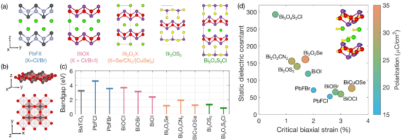
Crystal structure. The common structural feature of the family of materials is the presence of 2D distorted square-net units of [Bi2O2]2+ or [Pb2F2]2+ layers, whose structure bears strong similarity to that of the charge-neutral [Pb2O2] layers in litharge -PbO, as illustrated in Figure 1a and b. Specifically, in a [Bi2O2]2+ layer, a sheet of oxygen arranged in 2D square lattice is sandwiched between two sheets of bismuth, forming BiO4 square pyramids with the apexes alternatively pointing in the two layer-normal directions. Similar is the case for [Pb2F2]2+, where Pb and F replace Bi and O, respectively, and the structure is isoelectronic to [Bi2O2]2+. The nominal charges of Pb and Bi in the layers are 2+ and 3+, respectively, leaving both Pb2+ and Bi3+ with 6s2 lone-pair electrons. By stacking [Pb2F2]2+ or [Bi2O2]2+ with counter-anion layers such as Cl-, Br-, Se2-, CN-, [CuSe], [BiS2]-, or [BiS3]3-, a wide variety of mixed-anion layered materials can be formed, which all have a tetragonal lattice with an in-plane lattice constant in the range of 3.8–4.2 Å (see Figure 1a). The bonding within the [Pb2F2]2+ or [Bi2O2]2+ layers has a strong covalent character, whereas the bonding between the positively and negatively charged layers is mostly electrostatic in nature.
Excellent and highly tunable electronic properties. By varying the anion layers, the electronic bandgaps of the [Pb2F2]- and [Bi2O2]-based materials are highly tunable in the range of 0–5 eV, as shown in Figure 1c. For instance, in Bi5O4S3Cl, which is formed by combining two [Bi2O2]2+ layers with a [BiS3]- layer and a Cl- layer [19], the bandgap calculated by density functional theory (DFT) with the Heyd-Scuseria-Ernzerhof (HSE) hybrid functional [25] has a small value of 0.84 eV. In comparison, for BiOI and PbFBr, which are formed by stacking [Bi2O2]2+ or [Pb2F2]2+ layers with halide anion layers, the calculated bandgaps have much higher values of 2.37 eV and 3.55 eV, respectively. Importantly, these materials also have highly dispersive electronic bands. The calculated electron effective mass is as small as 0.14 in Bi2OS2 and 0.16 in Bi2O2Se, where is the free-electron mass. In Supplemental Figure S1, we present the DFT-calculated band structures of the [Pb2F2]- and [Bi2O2]-based materials. The methods of calculation are described in the Supporting Information, and the key structural and electronic structural information including the lattice parameters, bandgaps, and electron effective masses, are listed in Supplemental Table S1.
High polarizability and proximity to ferroelectric instability. Remarkably, the [Pb2F2]- and [Bi2O2]-based materials all have exceptionally high dielectric polarizability. As shown in Figure 1d, the in-plane static dielectric constant values , calculated for the materials at their experimental lattice constants via density functional perturbation theory (DFPT) [26], are all above 50 and can be as high as several hundreds. For instance, the value is 52.6 in PbFCl, 119.2 in BiOI, and 292.7 in Bi5O4S3Cl, which are all an order of magnitude higher than that of silicon (12.1) or GaAs (12.8) [8]. By comparing and the corresponding values listed in Supplemental Table S1, we conclude that the large static dielectric constants of the materials originate from high lattice polarizability, which indicates possible ferroelectric instability under a slightly changed lattice constants.
Indeed, we find that, by applying a small critical in-plane biaxial strain on the order of 0.5–3.5%, the inversion symmetry of the materials can be broken and a ferroelectric phase with non-zero in-plane electric polarization emerges. The directions of atomic displacements corresponding to the ferroelectric transitions are visualized for BiOCl in the inset of Figure 1d and for other materials in Supplemental Figure S2. The calculated critical biaxial strain are plotted together with in Figure 1d, where an overall inverse correlation between and can be observed. The strain-dependent potential energy landscape of BiOCl with respect to the ferroelectric atomic displacements exhibits a classical double-well structure beyond , as shown in Supplemental Figure S3, which is consistent with a second-order phase transition. The DFT-calculated electric polarizations of the ferroelectric phases of the family of materials at 2% of strain beyond are found to be between 15–35 , which are listed in Supplemental Table S1 and visualized in Figure 1d. In addition to biaxial strain, the ferroelectric transition can also be induced by in-plane uniaxial strain, and the associated critical strain values are slightly larger than those corresponding to biaxial strain and listed in Supplemental Table S1.
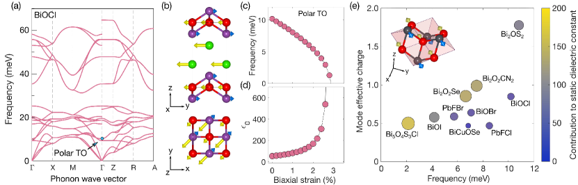
Origin of the high polarizability. The large family of [Pb2F2]- and [Bi2O2]-based highly polarizable semiconductors with excellent electronic properties, as well as their closeness to ferroelectric instability, prompt us to probe their fundamental origin. In Figure 2a we show the calculated phonon spectrum of BiOCl, which is taken as a representative member of the material family with . By inspecting the phonon modes near the center of the Brillouin zone, we find that an in-plane polar transverse optical (TO) phonon mode has a low frequency of 10 meV. By comparison, the lowest-frequency polar TO mode in GaAs has a much higher frequency of 33 meV [8]. The displacement pattern of the low-frequency polar TO mode of BiOCl is illustrated in Figure 2b, where the Bi atoms move out of phase with O and Cl atoms. By applying an in-plane biaxial strain, the polar TO mode rapidly softens (Figure 2c), accompanied by a divergent increase of as the critical point for ferroelectric instability is approached (Figure 2d). Thus, the large of BiOCl is strongly correlated with the presence of a low-frequency polar TO phonon mode.
More quantitatively, we calculate the contribution of each zone-center (wavevector ) phonon mode to the diagonal components of the static dielectric tensor , which is proportional to , where indicates a Cartesian direction, is the unit cell volume, the mode frequency, and is the mode effective charge vector that reflects the polarity of the zone-center phonon mode [9]. For a given mode, is calculated as the sum of the product of the Born effective charge (BEC) tensor and the mass-normalized eigendisplacement for each atom. For the tetragonal crystals studied here, the in-plane components of the mode effective charge vector can be written as , where is atomic index in the unit cell, the in-plane BEC, the atomic mass, the mass unit, and the phonon eigenvector (detailed discussions can be found in Supplementary Note S1).
By calculating the and for each zone-center phonon mode of BiOCl, we find that the lowest-frequency polar TO mode contributes more than 88% of the total in-plane lattice polarizability of BiOCl (Supplemental Table S2). In addition to the small mode frequency of 10 meV, the mode effective charge of the polar TO mode has a large value of 0.85, which is much larger than the corresponding value of 0.35 in GaAs. This is because BiOCl has large BECs, with the in-plane components equal to , , and for Bi, O, and Cl, respectively, which are all larger than the nominal charges of the elements in the compound. For comparison, the calculated for Ga and As in GaAs are 2.1 and for Ga and As, respectively. In Figure 2c, we compare the and of the lowest-frequency polar TO mode, as well as the contribution of the phonon mode to , for all the [Pb2F2]- and [Bi2O2]-based materials. The vibrational displacement patterns of the polar optical phonon modes are shown in Supplemental Figure S2, and the BECs in different materials are listed in Supplemental Table S3. As shown by Figure 2e, all the materials have small and large values, and the phonon mode that has a larger value also a larger contribution to the lattice polarizability. Thus, it is because the existence of a low-frequency polar optical phonon mode, as well as large BECs (which gives rise to large mode effective charge), that the [Pb2F2]- and [Bi2O2]-based materials have exceptionally high lattice polarizability.
Universal origin of ferroelectric instability. We next investigate why a low-frequency polar TO mode and large BECs are present in the [Pb2F2]- and [Bi2O2]-based materials, and why they are susceptible to strain-induced ferroelectric instability. Noticing that a common feature in these materials is the presence of [Pb2F2] or [Bi2O2] layered units that bears strong structural similarity to the charge-neutral [Pb2O2] layers in the litharge -PbO, we question whether the strain-induced ferroelectric instability can occur in -PbO as well. Intriguingly, we find that -PbO can also undergo ferroelectric transition upon imposing an in-plane biaxial or uniaxial strain, in both the bulk and monolayer form.
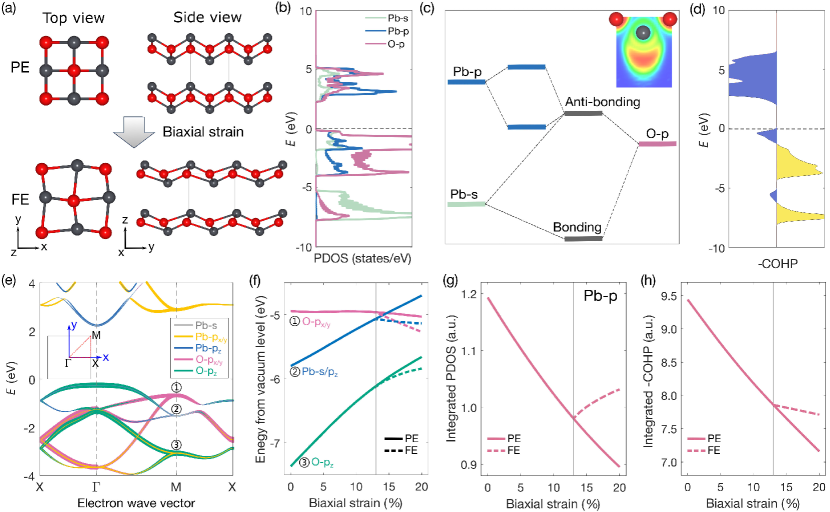
Figure 3a shows the top and side views of the paraelectric (PE) phase and biaxial strain-induced ferroelectric (FE) phases of -PbO. The unique distorted square-net structure in the PE phase is evident. The DFT-calculated critical biaxial strains to induce ferroelectric transition in bulk and monolayer -PbO are both around 13% (see Supplemental Figure S4). The atomic displacement pattern of ferroelectric displacement in -PbO bears a strong resemblance to those observed in the litharge-type layers of the [Pb2F2]- and [Bi2O2]-based materials.
The calculated projected density of states (PDOS) of monolayer -PbO, shown in Figure 3b, exhibits significant cross-bandgap hybridization of the Pb orbitals, This feature can be understood on the basis of the revised lone-pair model [27]. Due to the high electronegativity of oxygen and relativity-induced lowering of the Pb orbitals, the energy level of the O orbitals is lower than the Pb orbitals but higher than the Pb orbitals, which causes Pb cations to exist in a nominal charge state, keeping the lone-pair electrons. However, the Pb electrons are not chemically inert but interacting strongly with the O electrons. This leads to the formation of (Pb – O ) bonding and antibonding orbitals, and the electrons fill up to the antibonding level. By distorting the crystal structure through the displacement of Pb atoms in the out-of-plane directions of the Pb-O square net, the hybridization of the initially unoccupied Pb orbitals with the (Pb – O ) antibonding orbitals becomes symmetry allowed, resulting in the stabilization of the occupied antibonding electronic states, as illustrated in Figure 3c. The weakly antibonding character of the electronic states near the valence band maximum (VBM) is confirmed by the crystal orbital Hamilton population (COHP) analysis in Figure 3d.
Thus, it is the presence of lone-pair electrons in the cations and the unique distorted bonding geometry of the litharge-type structure that the Pb orbitals have strong cross-bandgap hybridization. These same bonding conditions are present within the [Pb2F2] and [Bi2O2] layers of the [Pb2F2]- and [Bi2O2]-based materials. Indeed, our DFT calculations confirm that significant cross-bandgap hybridization of the Pb or Bi orbitals also exist in the [Pb2F2]- and [Bi2O2]-based materials, as shown in Supplemental Figure S5. The same antibonding characters of the VBM of the materials are further shown in Supplemental Figure S6.
The strong cross-bandgap hybridization leads to large BECs in these materials, as listed in Supplemental Table S3. For example, the in-plane BECs of Pb and Bi in PbFBr and BiOI are 3.97 and 5.92, respectively, much higher than their respective nominal charges. This is because relative atomic distortion within the litharge-type layers of these materials can lead to a substantial change in the covalency of the occupied electronic states, as the participation of the unoccupied cation orbitals in the chemical bonding is susceptible to the bonding geometry and environment. According to the soft-mode theory of Cochran [28], the softening of polar TO mode is driven by the competition between long-range Coulomb interaction, which favors a distorted low-symmetry ferroelectric phase, and short-range forces, which favors the high-symmetry paraelectric phase. Large BECs lead to a more significant contribution of the long-range Coulomb interaction, resulting in reduced restoring force and thus a low-frequency polar TO mode. By applying tensile strain to the system, the short-range bonding interaction can be weakened, due to an overall decrease in inter-atomic electronic hybridization. Thus, as the amount of tensile strain is increased, the frequency of polar TO modes in materials with large BECs can be further reduced and eventually become completely softened, resulting in a ferroelectric transition [29, 24].
Another perspective to understand the strain-induced ferroelectric transition is that the ferroelectric displacements of the Pb or Bi cations can compensate the strain-induced weakening of chemical bonds through enhanced participation of the unoccupied cation orbital in the stabilization of the antibonding valence states. This is supported by our calculation of the strain-dependent electronic structure evolution of monolayer -PbO. Figure 3e shows the calculated electronic band structure of monolayer -PbO, where three electronic state at the M-point are indicated. As the imposed in-plane biaxial strain is increased, it is observed that the electronic states with initially substantial admixture of Pb orbitals rapidly rise in energy (Figure 3f), as the stabilization effect of the Pb orbital is weakened due to increased interatomic distances. This is reflected in Figure 3g and Figure 3h, where rapid decreases in the calculated integrated PDOS of Pb orbitals in the valence manifold and the integrated COHP values can be seen. Beyond the critical strain of 13%, the lateral distortion of the Pb atoms in the ferroelectric phase can reverse the trend of the participation of Pb orbitals in the bonding (Figure 3g), which leads to a slowed weakening in the total bonding strength (Figure 3h), as well as energy gain with respect to the paraelectric phase.
Compared to monolayer -PbO, the mixed-anion, quasi-layered structure of the [Pb2F2]- and [Bi2O2]-based materials with additional counter-anion layers in between the [Pb2F2] or [Bi2O2] layers further reduces the overall short-range forces that inhibit the softening of the polar TO phonons. As shown in Figure 2b and Supplemental Figure S2, the polar TO phonons in these materials involve not only the internal displacements within the [Pb2F2] or [Bi2O2] layers, but also the relative displacements between the litharge-type layers and the counter-anion layers. Unlike the strong covalent bonding within the litharge-type [Pb2F2] or [Bi2O2] layers, the bonding between the counter-anion layers and the litharge-type layers has a weak covalent character and is more electrostatic in origin. In addition, the smaller bandgaps of the [Bi2O2]-based materials lead to their stronger cross-bandgap hybridization (Supplemental Figure S5), which results in larger BECs (Supplemental Table S3) and stronger long-range Coulomb interactions. Consequently, the [Pb2F2]- and [Bi2O2]-based materials have a reduced critical tensile strain (between 0.5% to 3%) needed for the complete softening of the polar TO mode and thus the ferroelectric transition.
Conclusions and outlook. In conclusion, we discover that a large family of [Pb2F2]- and [Bi2O2]-based mixed-anion materials with a litharge-type structural unit are highly polarizable layered semiconductors with structural diversity, a wide range of bandgaps (0–5 eV), and excellent electronic properties, making them attractive for applications in electronics and optoelectronics based on layered and 2D materials. We further uncover the fundamental origin of their high lattice polarizability by revealing the crucial roles of cation lone-pair electrons and cross-bandgap electronic hybridization in the presence of a low-frequency polar TO phonon mode in their lattice dynamics. Our results indicate that proximity to strain-induced ferroelectricity is a universal phenomenon in [Pb2F2]- and [Bi2O2]-based compounds with a litharge-type structural unit, opening a large chemical space for designing novel ferroelectric and incipient ferroelectric materials, whose bandgaps can be varied from infrared to ultraviolet spectrum by choosing proper counter-anion layers.
Importantly, the crystal symmetries and lattice constants of the [Bi2O2]- and [Pb2F2]-based materials have close match with each other and with the perovskite family of materials such as SrTiO3 and LaAlO3. Thus, a large variety of novel heterostructures can be constructed by stacking [Bi2O2]- and [Pb2F2]-based materials with each other, or with the perovskite oxides, offering rich heterostructural design freedom, especially given the highly chemically tunable bandgaps of the [Bi2O2]- and [Pb2F2]-based materials. Due to the close proximity of the materials to ferroelectric transition, the mismatch strain at the heterostructural interface could be sufficient to induce ferroelectricity, while the polar discontinuity at the heterostructural interface may causes carrier doping [30], which could lead to the coveted polar metallic phase [31, 32] in such heterostructures. Notably, in degenerately doped [Bi2O2]-based compounds, superconductivity has been experimentally reported [16, 17, 18, 19]. Thus, it is also possible that the long-sought coexistence of ferroelectricity and superconductivity could be realized in this large family of materials and their heterostructures. In summary, the [Bi2O2]- and [Pb2F2]-based materials with a litharge-type structural unit offer an exciting playground for designing high performance and highly polarizable layered semiconductors, as well as novel ferroelectric heterostructures, with vast potential to uncover exotic solid state phenomena for emerging technologies.
Acknowledgments. The work of Z.Z., J.H., Y.Y., and W.L. is supported by the National Natural Science Foundation of China (NSFC) under Grant No. 62374136. W.L. also acknowledges the support by Research Center for Industries of the Future at Westlake University under Award No. WU2022C041. X.L. acknowledges the support by “Pioneer” and “Leading Goose” RD Program of Zhejiang under Grant 2024SDXHDX0007, Zhejiang Provincial Natural Science Foundation of China for Distinguished Young Scholars under Grant No. LR23A040001, and the NSFC under Grant No. 12474131. H.W. acknowledges the support from the NSFC under Grant Nos. 12304049 and 12474240. The authors thank Prof. S.H. Wei for inspiring discussions and the HPC center of Westlake University for computational support. Z. Zhu and J. Hu contributed equally.
References
- Jaramillo and Ravichandran [2019] R. Jaramillo and J. Ravichandran, In praise and in search of highly-polarizable semiconductors: Technological promise and discovery strategies, APL Materials 7, 100902 (2019).
- Ashcroft and Mermin [1976] N. W. Ashcroft and N. D. Mermin, Introduction to Solid State Physics (Saunders, Philadelphia, 1976).
- Zhu et al. [2016] H. Zhu, K. Miyata, Y. Fu, J. Wang, P. P. Joshi, D. Niesner, K. W. Williams, S. Jin, and X.-Y. Zhu, Screening in crystalline liquids protects energetic carriers in hybrid perovskites, Science 353, 1409–1413 (2016).
- Zhu et al. [2022] Z. Zhu, X. Yao, S. Zhao, X. Lin, and W. Li, Giant modulation of the electron mobility in semiconductor Bi2O2Se via incipient ferroelectric phase transition, J. Am. Chem. Soc. 144, 4541 (2022).
- He et al. [2018] X. He, D. J. Singh, P. Boon-on, M.-W. Lee, and L. Zhang, Dielectric behavior as a screen in rational searches for electronic materials: metal pnictide sulfosalts, J. Am. Chem. Soc. 140, 18058–18065 (2018).
- Li et al. [2021] W. Li, X. Qian, and J. Li, Phase transitions in 2D materials, Nat. Rev. Mater. 6, 829 (2021).
- Wu et al. [2023] M. Wu, Z. Lou, C. Dai, T. Wang, J. Wang, Z. Zhu, Z. Xu, T. Sun, W. Li, X. Zheng, and X. Lin, Achieving ferroelectricity in a centrosymmetric high‐performance semiconductor by strain engineering, Adv. Mater. 35, 2300450 (2023).
- Madelung [2004] O. Madelung, Semiconductors: Data Handbook (Springer-Verlag Berlin Heidelberg, 2004).
- Gonze and Lee [1997] X. Gonze and C. Lee, Dynamical matrices, Born effective charges, dielectric permittivity tensors, and interatomic force constants from density-functional perturbation theory, Phys. Rev. B 55, 10355 (1997).
- Filippone et al. [2020] S. Filippone, B. Zhao, S. Niu, N. Z. Koocher, D. Silevitch, I. Fina, J. M. Rondinelli, J. Ravichandran, and R. Jaramillo, Discovery of highly polarizable semiconductors BaZrS3 and Ba3Zr2S7, Phys. Rev. Mater. 4, 091601 (2020).
- Liang et al. [2021] Y. Liang, X. Zhou, W. Li, and H. Peng, Preparation of two-dimensional [Bi2O2]-based layered materials: Progress and prospects, APL Materials 9, 060905 (2021).
- Bannister [1935] F. A. Bannister, The crystal-structure of the bismuth oxyhalides, Mineral. Mag. 24, 49 (1935).
- Boller [1973] H. Boller, Die kristallstruktur von Bi2O2Se, Monatshefte für Chemie 104, 916 (1973).
- Corkett et al. [2019] A. J. Corkett, Z. Chen, D. Bogdanovski, A. Slabon, and R. Dronskowski, Band gap tuning in bismuth oxide carbodiimide Bi2O2NCN, Inorg. Chem. 58, 6467 (2019).
- Zhao et al. [2014] L.-D. Zhao, J. He, D. Berardan, Y. Lin, J.-F. Li, C.-W. Nan, and N. Dragoe, BiCuSeO oxyselenides: new promising thermoelectric materials, Energy Environ. Sci. 7, 2900 (2014).
- Phelan et al. [2013] W. A. Phelan, D. C. Wallace, K. E. Arpino, J. R. Neilson, K. J. Livi, C. R. Seabourne, A. J. Scott, and T. M. McQueen, Stacking variants and superconductivity in the Bi–O–S system, J. Am. Chem. Soc. 135, 5372 (2013).
- Ruan et al. [2019] B.-B. Ruan, K. Zhao, Q.-G. Mu, B.-J. Pan, T. Liu, H.-X. Yang, J.-Q. Li, G.-F. Chen, and Z.-A. Ren, Superconductivity in Bi3O2S2Cl with Bi–Cl planar layers, J. Am. Chem. Soc. 141, 3404–3408 (2019).
- Zou et al. [2023] X. Zou, M. Xie, R. Wang, H. Liang, Y. Li, F. Tian, Y. Sun, and C. Wang, Two-dimensional superconductivity in air-stable single-crystal few-layer Bi3O2S3, J. Am. Chem. Soc. 145, 20975–20984 (2023).
- Yang et al. [2023] Y. Yang, X. Fan, J. Liu, C. Cao, Z. Liu, J. Deng, T. Lin, Q. Zhang, K. Liao, X. Dong, G. Wang, and X. Chen, Discovery of a superconductor Bi5O4S3Cl containing the unique BiS3 layer, Adv. Sci. 10, 2303569 (2023).
- Cheema et al. [2020] S. S. Cheema, D. Kwon, N. Shanker, R. dos Reis, S.-L. Hsu, J. Xiao, H. Zhang, R. Wagner, A. Datar, M. R. McCarter, C. R. Serrao, A. K. Yadav, G. Karbasian, C.-H. Hsu, A. J. Tan, L.-C. Wang, V. Thakare, X. Zhang, A. Mehta, E. Karapetrova, R. V. Chopdekar, P. Shafer, E. Arenholz, C. Hu, R. Proksch, R. Ramesh, J. Ciston, and S. Salahuddin, Enhanced ferroelectricity in ultrathin films grown directly on silicon, Nature 580, 478–482 (2020).
- Cheema et al. [2022] S. S. Cheema, N. Shanker, S.-L. Hsu, Y. Rho, C.-H. Hsu, V. A. Stoica, Z. Zhang, J. W. Freeland, P. Shafer, C. P. Grigoropoulos, J. Ciston, and S. Salahuddin, Emergent ferroelectricity in subnanometer binary oxide films on silicon, Science 376, 648–652 (2022).
- Yasuda et al. [2024] K. Yasuda, E. Zalys-Geller, X. Wang, D. Bennett, S. S. Cheema, K. Watanabe, T. Taniguchi, E. Kaxiras, P. Jarillo-Herrero, and R. Ashoori, Ultrafast high-endurance memory based on sliding ferroelectrics, Science 385, 53–56 (2024).
- Bian et al. [2024] R. Bian, R. He, E. Pan, Z. Li, G. Cao, P. Meng, J. Chen, Q. Liu, Z. Zhong, W. Li, and F. Liu, Developing fatigue-resistant ferroelectrics using interlayer sliding switching, Science 385, 57–62 (2024).
- Cao et al. [2024] R. Cao, Q.-L. Yang, H.-X. Deng, S.-H. Wei, J. Robertson, and J.-W. Luo, Softening of the optical phonon by reduced interatomic bonding strength without depolarization, Nature 634, 1080–1085 (2024).
- Heyd et al. [2003] J. Heyd, G. E. Scuseria, and M. Ernzerhof, Hybrid functionals based on a screened Coulomb potential, J. Chem. Phys. 118, 8207 (2003).
- Baroni et al. [2001] S. Baroni, S. de Gironcoli, A. Dal Corso, and P. Giannozzi, Phonons and related crystal properties from density-functional perturbation theory, Rev. Mod. Phys. 73, 515 (2001).
- Walsh et al. [2011] A. Walsh, D. J. Payne, R. G. Egdell, and G. W. Watson, Stereochemistry of post-transition metal oxides: revision of the classical lone pair model, Chem. Soc. Rev. 40, 4455 (2011).
- Cochran [1959] W. Cochran, Crystal stability and the theory of ferroelectricity, Phys. Rev. Lett. 3, 412 (1959).
- Cohen [1992] R. E. Cohen, Origin of ferroelectricity in perovskite oxides, Nature 358, 136–138 (1992).
- Zhu et al. [2023] Z. Zhu, J. Qi, X. Zheng, X. Lin, and W. Li, Polar discontinuities and interfacial electronic properties of Bi2O2Se on SrTiO3, Phys. Rev. B 108, 245304 (2023).
- Anderson and Blount [1965] P. W. Anderson and E. I. Blount, Symmetry considerations on Martensitic transformations: “Ferroelectric” metals?, Phys. Rev. Lett. 14, 217 (1965).
- Bhowal and Spaldin [2023] S. Bhowal and N. A. Spaldin, Polar metals: Principles and prospects, Annu. Rev. Mater. Res. 53, 53–79 (2023).