Observation of the dual quantum spin Hall insulator by density-tuned correlations in a van der Waals monolayer
Abstract
The convergence of topology and correlations represents a highly coveted realm in the pursuit of novel quantum states of matter [2, 3]. Introducing electron correlations to a quantum spin Hall (QSH) insulator can lead to the emergence of a fractional topological insulator and other exotic time-reversal-symmetric topological order [4, 5, 6, 7, 8, 9, 10, 11], not possible in quantum Hall and Chern insulator systems. However, the QSH insulator with quantized edge conductance remains rare, let alone that with significant correlations. In this work, we report a novel dual QSH insulator within the intrinsic monolayer crystal of TaIrTe4, arising from the interplay of its single-particle topology and density-tuned electron correlations. At charge neutrality, monolayer TaIrTe4 demonstrates the QSH insulator that aligns with single-particle band structure calculations, manifesting enhanced nonlocal transport and quantized helical edge conductance. Interestingly, upon introducing electrons from charge neutrality, TaIrTe4 only shows metallic behavior in a small range of charge densities but quickly goes into a new insulating state, entirely unexpected based on TaIrTe4’s single-particle band structure. This insulating state could arise from a strong electronic instability near the van Hove singularities (VHS), likely leading to a charge density wave (CDW). Remarkably, within this correlated insulating gap, we observe a resurgence of the QSH state, marked by the revival of nonlocal transport and quantized helical edge conduction. Our observation of helical edge conduction in a CDW gap could bridge spin physics and charge orders. The discovery of a dual QSH insulator introduces a new method for creating topological flat minibands via CDW superlattices, which offer a promising platform for exploring time-reversal-symmetric fractional phases and electromagnetism [4, 12, 5, 12, 6, 13].
Introduction
Topology and correlations are two central themes of current condensed matter research [14, 3]. Their interplay gives rise to correlated topological phases [2], including topological order, which could lead to phenomena such as topological fractionalization, long-range entanglement, and non-Abelian anyons. Recent theory developments have highlighted materials exhibiting both single-particle topological bands and strong correlations as exciting candidates to explore in the search for correlated topological phases [15, 16, 17, 18]. An intriguing but rarely explored scenario is “QSH + correlations”, i.e., to introduce correlations to the band of a QSH insulator [14]. The time-reversal symmetry present for the band can enable time-reversal-symmetric topological order such as the fractional QSH and the helical quantum spin liquid [4, 5, 12, 6, 7, 8, 9, 10, 11], unattainable in quantum Hall [19] and Chern insulators [20, 21, 22, 23, 24].
Despite the fundamental interest in this “QSH + correlations” scenario, it is rarely investigated due to the scarcity of suitable material platforms. First, while the QSH state has been explored in many materials [25, 26, 27, 28, 29, 30, 31, 32, 33, 34, 35, 36, 37, 38], achieving the QSH effect with quantized helical edge conduction has been extremely rare [26, 31, 39, 40]. Second, it is even rarer to find a QSH insulator exhibiting strong correlations, as most QSH materials have dispersive bands. One effective way to induce strong correlations involves achieving a large density of states via the van Hove singularity (VHS) (Fig. 1a-b), a strategy that has resurged in recent studies of graphene and kagome materials [41, 42, 43, 44]. In this work, we report a new electronic phenomenon that arises from the interplay of QSH topology and VHS-induced correlations, the dual QSH insulator, in a vdW monolayer crystal TaIrTe4. Specifically, we detect two distinct charge gaps: one at charge neutrality and another near the DFT-calculated VHS positions (Fig. 1c). Each gap exhibits QSH helical edge conduction, named as QSH-I and QSH-II, respectively. Our systematic study shows that while QSH-I represents a single-particle QSH effect, QSH-II is a correlated QSH, likely arising from a topological CDW that unusually links spin transport with charge order. Moreover, this dual QSH reveals a flat QSH band, which holds promise for exploring time-reversal invariant fractional phases.
Lattice and electronic structures of monolayer TaIrTe4
Bulk TaIrTe4 is a layered (Fig. 1d) Weyl semimetal that has been investigated in both theoretical and experimental studies [45, 46, 47, 48, 36, 49]. In contrast, monolayer TaIrTe4 has not yet been experimentally explored, due to its severe air-sensitivity and the challenges associated with exfoliation. By systematically optimizing the fabrication conditions (Methods), we have successfully accessed the intrinsic electronic properties of monolayer TaIrTe4 for the first time (see Extended Data Fig. 1 and Supplementary Information (SI) Section 1).
Structurally, monolayer TaIrTe4 features 1D Ta and Ir chains along the crystalline axis (Fig. 1e). Within a single unit cell, there are two inequivalent Ta (Ir) chains, which are related by a rotation about the axis () (Fig. 1e). Observing the - plane, the monolayer is made of alternating parallelograms - one parallelogram is formed by two Ta and two Te while the other is formed by two Ir and two Te. In terms of electronic properties, theoretical predictions suggest that monolayer TaIrTe4 is a QSH insulator with a substantial band gap [50, 51]. Notably, our calculations also reveal prominent VHS close to the single-particle QSH gap, as indicated by the bright intensity spots inside the projected bulk bands in Fig. 1c. We will revisit this lattice and electronic structures, as it proves crucial for understanding our observations.
Unconventional basic transport characteristics of monolayer TaIrTe4
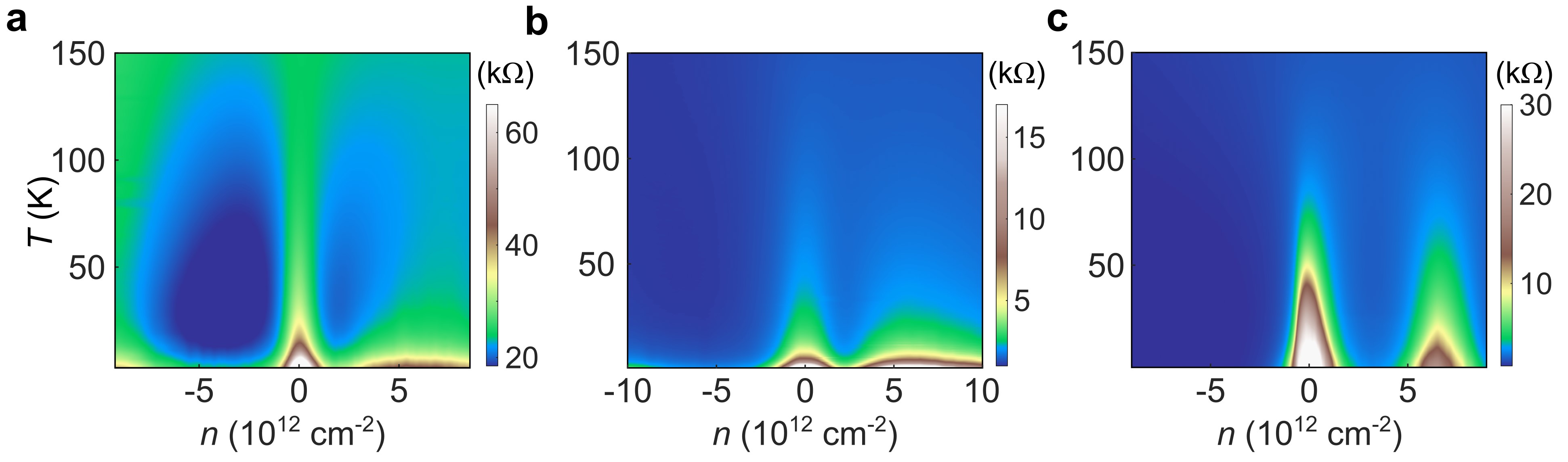
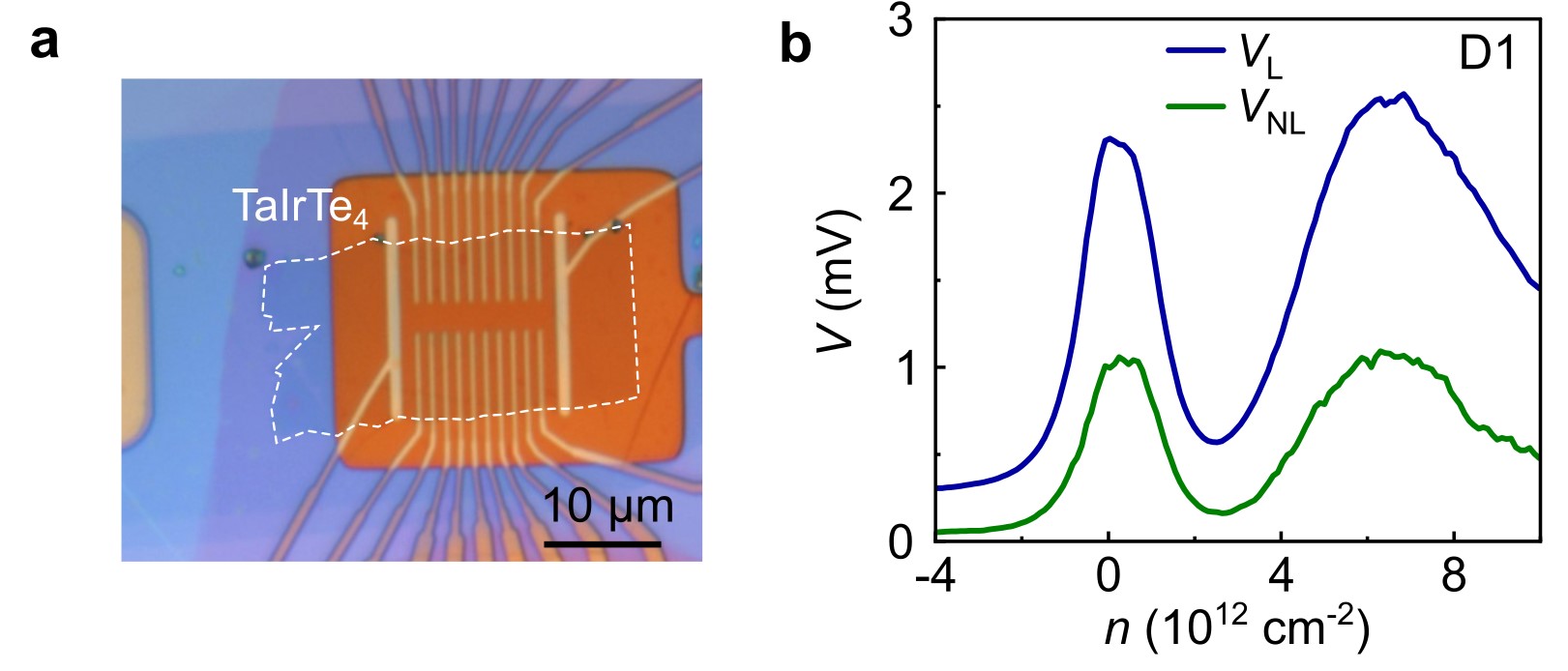
We have fabricated high-quality dual-gated (top gate voltage, and bottom gate voltage, ) monolayer TaIrTe4 devices. We observed highly consistent behaviors across over a dozen devices. Transport characterizations conducted on 19 devices indicate mobility ranging from approximately 10 to 400 cm2/(Vs) (SI 1.4). Figure 1f shows the four-probe resistance as a function of the carrier density (see electric field dependence and discussions in SI 4.2 and 5.2). Notably, even for this basic property, monolayer TaIrTe4 already distinctly differs from known QSH systems including monolayer WTe2 [34, 39]. Specifically, in addition to the resistance peak at charge neutrality which is expected based on the single-particle band structure, we observe a second resistance peak in the electron-doped regime at cm-2 (Fig. 1f-g). Below, we systematically study both resistive peaks.
Observation of single-particle QSH state at charge neutrality
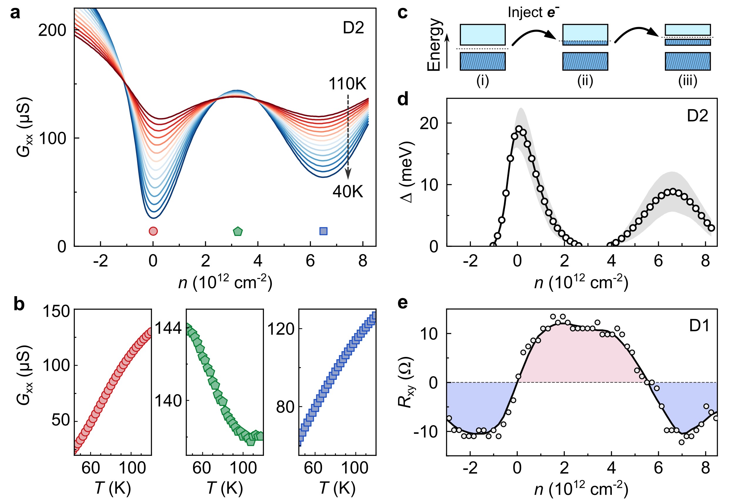
We first study the physics associated with the resistance peak at the charge neutrality point (CNP). As shown in Fig. 2a, the CNP conductance decreases with decreasing temperature and expands into a plateau below 30 K, suggesting a band gap. Also, the conductance saturates at a nonzero value denoted as in Fig. 2a, hinting at an additional in-gap conduction channel. Importantly, the conductance of this plateau is S, approaching ( S). To estimate the magnitude of the band gap, we apply the thermal-activation fit to the temperature-dependent conductance at CNP (with and without subtracting ) (Fig. 2b). The fitting yields an activation gap between 20 to 30 meV, which approximately aligns with the first-principles calculated gap at the CNP (Fig. 1c). In SI 1.4, we further extracted the gap size on devices in which the edge channels are physically covered.
The finite conductance plateau at the CNP suggests in-gap states, which could arise from edge states or bulk defect states. To gain further insight, we performed nonlocal transport measurements, previously proven effective in studying QSH systems [52, 34] in which significant nonlocal voltage, , arises from the edge conduction around the outer boundary of the sample (Fig. 2c). In our measurements, is prominent within the band gap and suppressed outside the gap (Fig. 2d). Moreover, we found negligible when the edge contribution was eliminated by physically covering the edge with an insulating boron nitride (BN) flake (Extended Data Fig. 5). These observations suggest that the finite conductance plateau in Fig. 2a originates from edge state conduction.
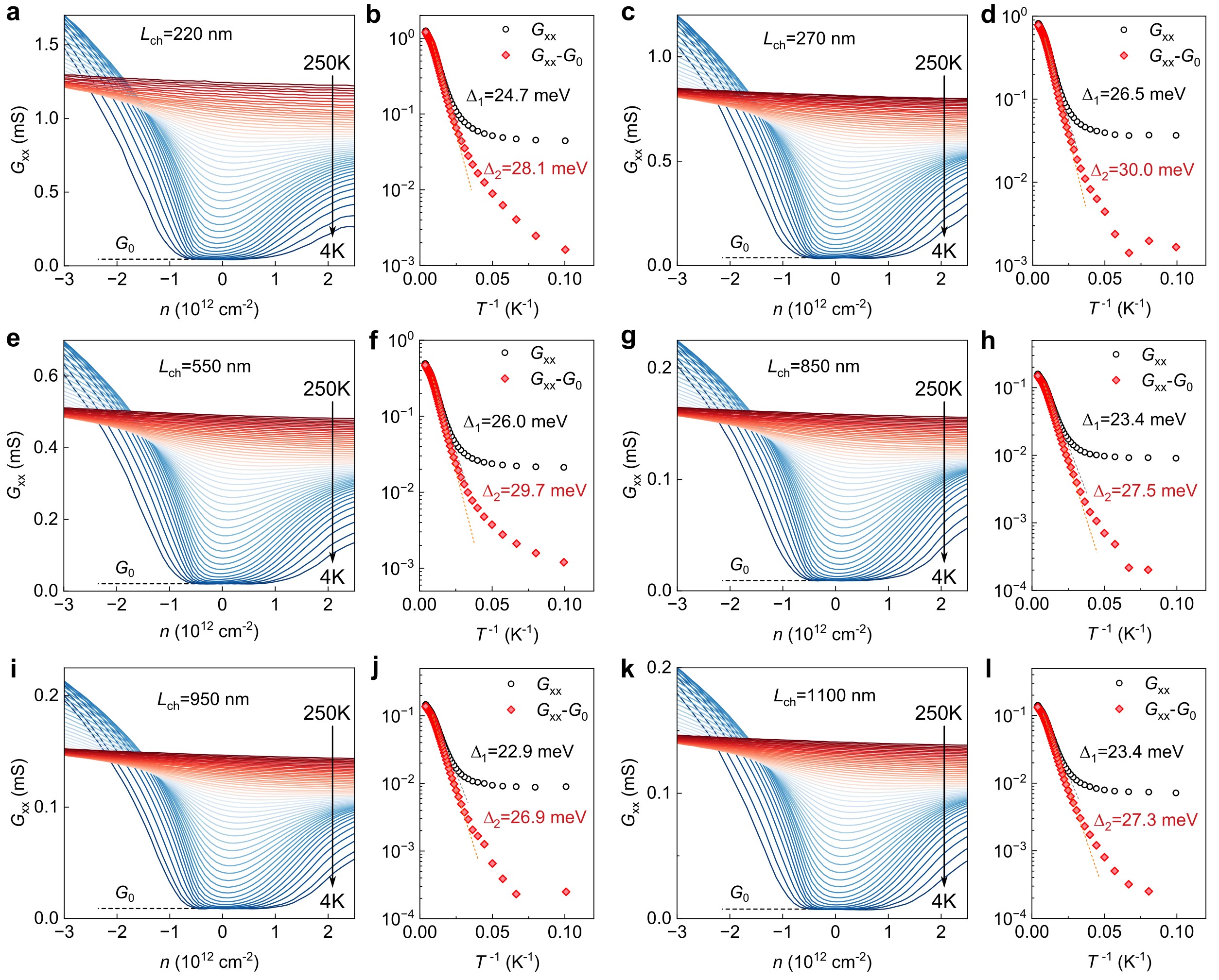
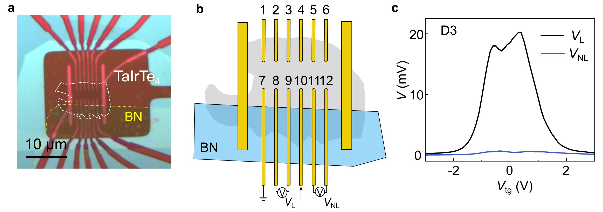
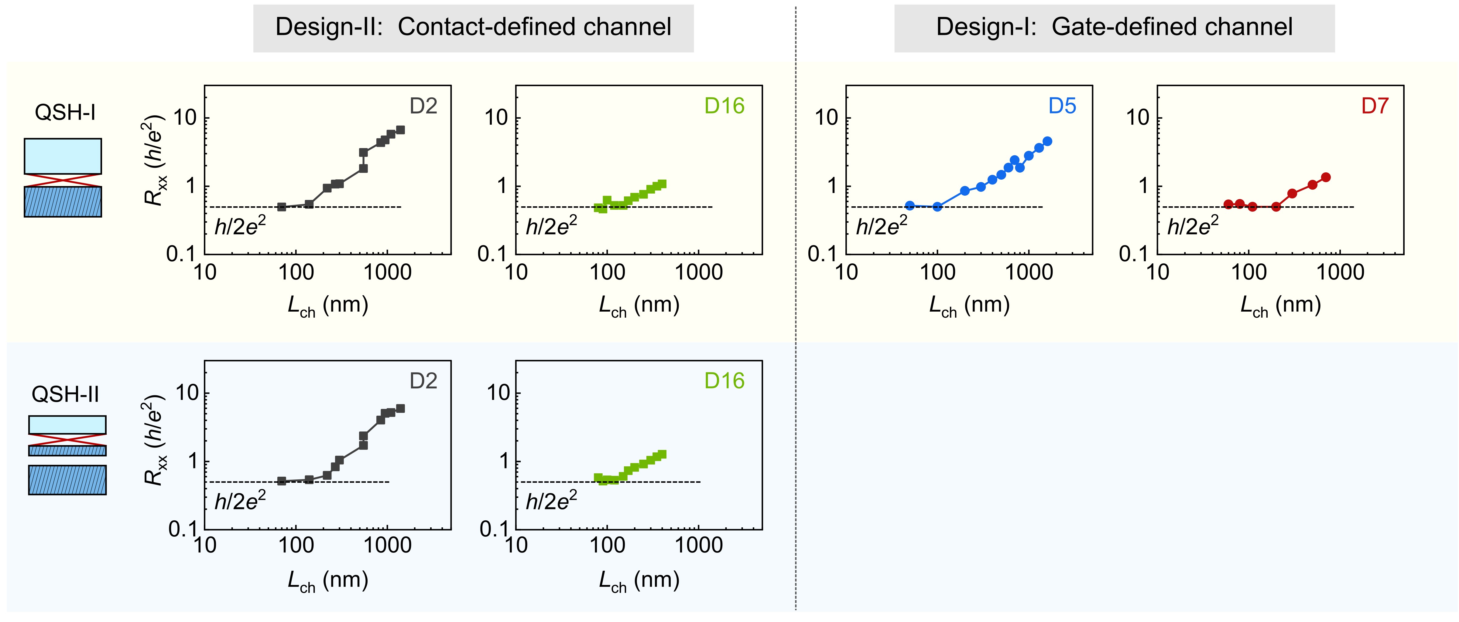
We now study the nature of the edge states (topological or trivial). A defining characteristic of QSH is the quantized conductance of ( per edge) in the short-channel (ballistic) regime [26, 31, 39, 40]. Therefore, we now investigate the edge conduction versus the channel length via two device designs. In Design-I, a strategy previously utilized in WTe2 [39], we apply the global top gate to heavily dope the sample and adjust the local bottom gate to neutralize the charge, effectively setting as the width of the designated local bottom gate (Fig. 2e). In Design-II, the channel is more directly defined between adjacent metal contacts (Fig. 2f). Both designs yielded consistent results in our case: the resistance (conductance) decreases (increases) as decreases. Upon entering the short-channel regime, the resistance (conductance) approaches and levels off at the quantized value of () regardless of the channel width (Fig. 2g). The edge quantization exhibits minimal dependence on current biasing within 100 nA (SI 2.2), suggesting ohmic contacts to the edge channels. The quantization channel length typically ranges from 100 to 200 nm, with our highest-performing sample extending up to 380 nm. Beyond this length, conductance may still saturate to a value on the order of below 30 K (Extended Data Fig. 4), implying minimal bulk contribution. This suggests that deviations from quantization are likely due to inelastic edge scattering [53, 54] rather than bulk residual channels.
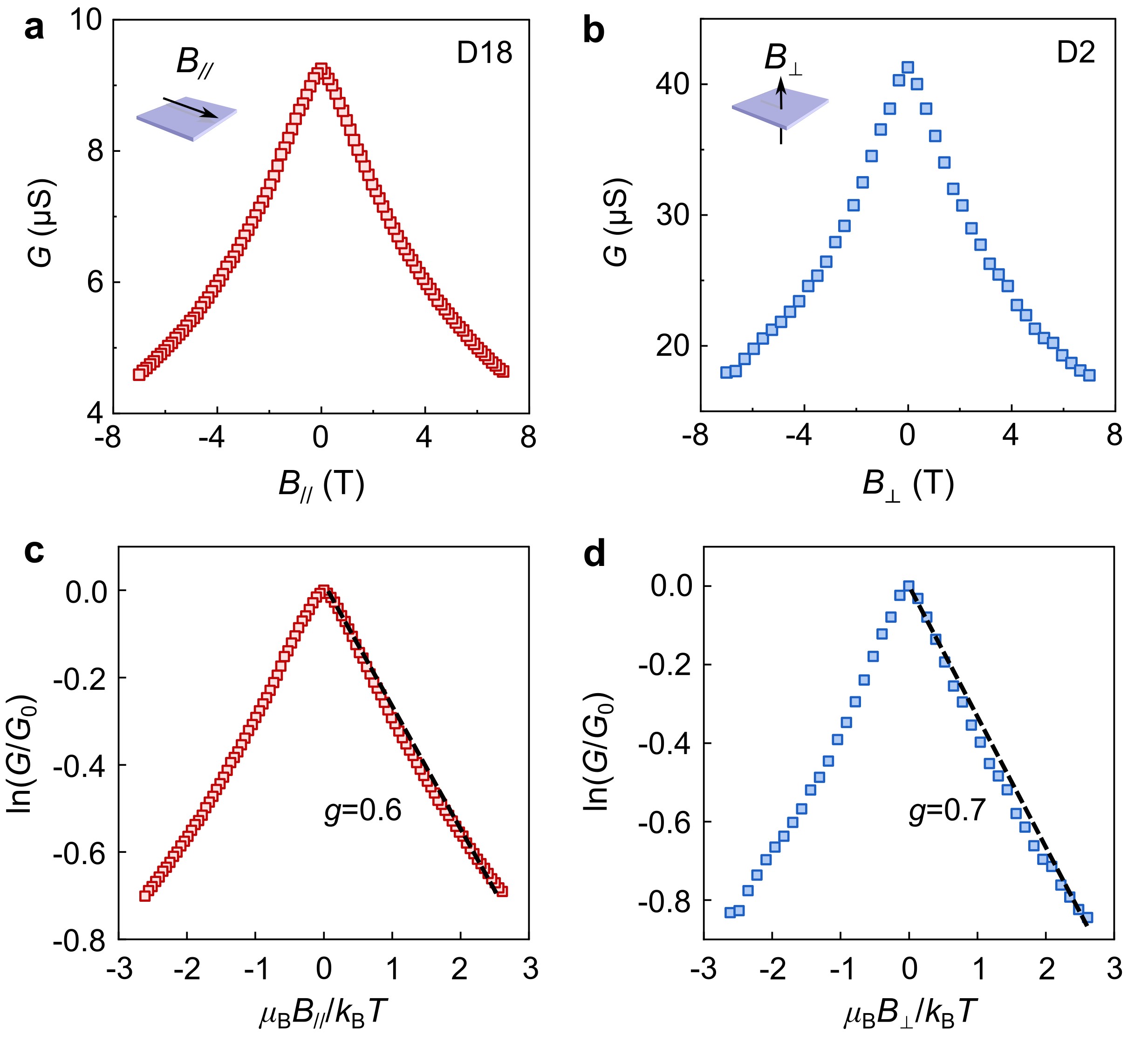
We conducted further investigations into the magnetic field dependence of the edge conduction [55, 56]. Our data show that the edge conduction is weakly suppressed by applying magnetic field (Extended Data Fig. 7). We propose an explanation based on our DFT calculation shown in Fig. 1c: the edge Dirac point resides within the valence band of the bulk, making it impossible to position the chemical potential solely within the magnetic gap, leading to a weak magnetic field response (See SI 2.5 for more detailed discussions).
Unexpected insulating states at finite dopings
We now turn our attention to investigating the resistance peak in the electron-doped regime, which contradicts the expectations based on the single-particle band structure. Extrinsically, this second resistance peak may be due to disorder-induced localization [57], while intrinsically, it may arise from the opening of an energy gap at a specific chemical potential due to electron correlations. To explore this further, we present the temperature-dependent conductance across a wider range of carrier densities in Fig. 3a as well as in Extended data Fig. 3. At CNP (), the temperature dependence displays insulating behavior (Fig. 3b, red curve), consistent with the CNP single-particle gap. As we increase the carrier density to cm-2, the temperature dependence becomes metallic (green curve). Further increasing to cm-2 results in insulating behavior once again (blue curve). In a typical scenario, if disorder played a significant role in inducing insulating behavior at cm-2, it should similarly result in insulating behavior at lower carrier densities such as cm-2. Figure 3d shows the fitted activation gap as a function of carrier density .
We also performed Hall measurements at an elevated temperature of 60 K. We observed not only the expected sign reversal of the Hall signal at the CNP but also a second sign reversal near the resistive feature at cm-2 (Fig. 3e). This additional sign reversal could arise from the emergence of hole-like pockets, consistent with the existence of VHS (Fig. 1c and additional data and analysis in SI 3.1-3.3). Collectively, we propose the following explanation for the double resistance peaks observed in Fig. 1f: The first resistance peak at CNP represents a single-particle gap. Upon electron doping to a certain level, a correlated gap appears from enhanced correlations near the VHS, as illustrated in Fig. 3c.
Observation of a second QSH state - TaIrTe4 is a dual QSH insulator
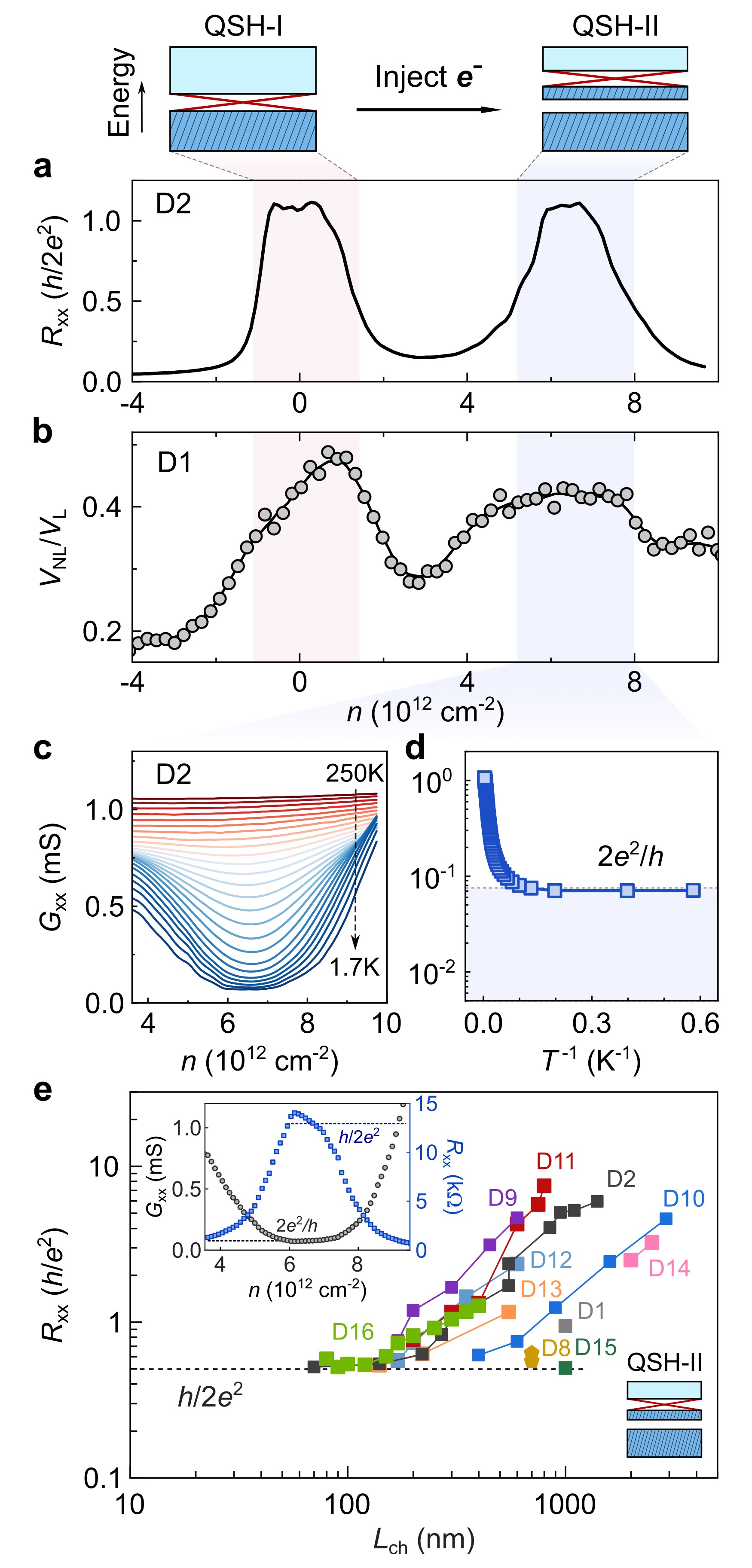
Before moving to more in-depth theoretical considerations, we now explore the topological nature of the emergent insulating state. This is particularly interesting since the new insulating gap occurs at a low filling ( cm-2) of the QSH conduction band. Our initial findings revealed that the ratio between and is significant within both the CNP single-particle gap and the second insulating gap while suppressed elsewhere (Fig. 4a-b). This indicates that edge conduction is present within the second gap as well.
To definitively discern if the second insulating state is topological or trivial, we proceeded to measure the conductance of short-channel devices. In Fig. 4c-d, we investigate the temperature-dependent conductance of a fixed short channel length ( nm) in the vicinity of the second insulating gap. As the temperature decreases, we observe that the conductance stabilizes at a plateau of . We further investigate the channel length dependence of the conductance at the second gap. As shown in Fig. 4e, the resistance (conductance) decreases (increases) with decreasing the channel length . Upon entering the short-channel regime, the resistance (conductance) levels off at the quantized value of (). We also examined the dependence on the magnetic field, which shows a conductance suppression by magnetic field similar to that for the CNP state (SI 4.3). In conclusion, we establish that the second insulating gap also exhibits the QSH state with quantized helical edge conduction.
Beyond the quantized conduction, we have further conducted spin valve experiments [58]. Our results, provided in SI 4.5, indicate that the edge currents within both insulating gaps carry spin. Collectively, we provide strong evidence that monolayer TaIrTe4 is a novel dual QSH insulator, which consists of two QSH states, both featuring the hallmark helical quantized edge conduction (Fig. 4a): one is the consequence of the single-particle topology at CNP and the other may arise from enhanced correlations at finite dopings. The two QSH states can be switched back and forth by tuning the carrier density via gating.
Theoretical understanding of the dual QSH state
We now provide theoretical analyses and present a tentative framework to understand the observed dual QSH insulator state. We outline our theoretical understanding in a step-by-step manner as follows.
First, we study the single-particle band structure to understand the QSH at charge neutrality. Our first-principles calculations have revealed that the low-energy electronic states primarily originate from the Ta 5 orbitals (see Extended Data Fig. 9 and SI 5.1). The presence of two inequivalent Ta atoms results in two distinct bands, and the fact that they are related by the symmetry implies that these two bands will exhibit Dirac crossings (see Extended Data Fig. 10). Indeed, our calculations on monolayer TaIrTe4 show two Dirac cones at the points without spin-orbit coupling (SOC). The inclusion of SOC gaps the Dirac point, giving rise to the QSH insulating state (see SI 5.1).
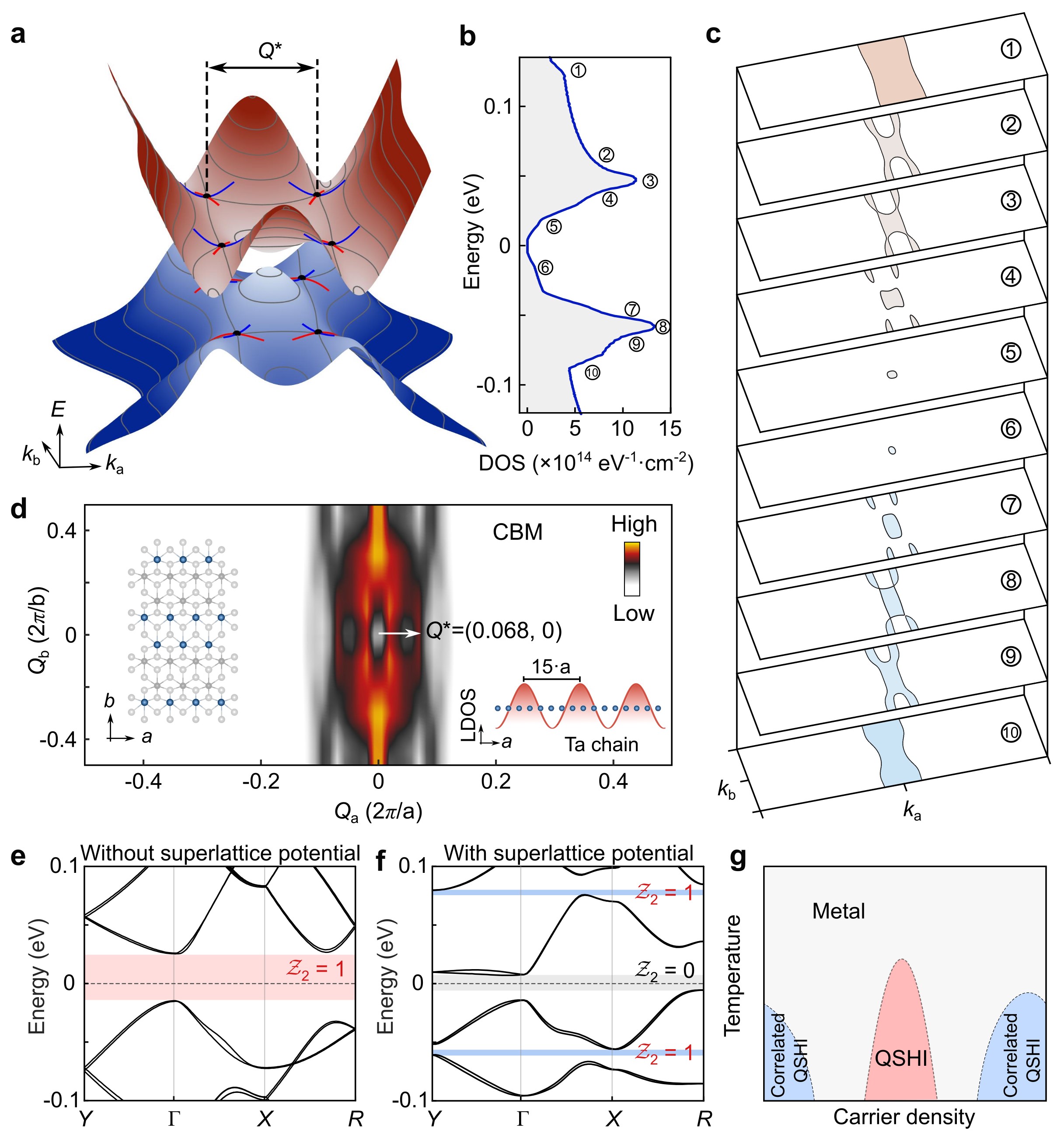
Second, our calculations revealed saddle-point VHS inside the conduction (valence) band. Monolayer TaIrTe4 has three low-energy Fermi pockets with direct gaps (Fig. 5a) - Two arise from the gapped Dirac cones at , while the third comes from an additional pocket at . As one increases energy, these pockets are found to gradually expand and merge into saddle points in the conduction and valence bands, giving rise to VHS (Figs. 5a-c). Interestingly, our calculations indicate that achieving the VHS on the hole side requires a higher carrier density. Consequently, we might also expect to observe a VHS-induced correlated insulating peak on the hole side, but this would necessitate reaching higher gate voltages on the hole side. Currently, our data only shows a slight increase in resistance on the hole side, as shown in Fig. 1f.
Third, we attempt to understand the emergent insulating state. Based on the carrier density, the absence of evidence for magnetism, and the value of quantized edge conductance associated with the correlated insulating gap, we identify charge density wave (CDW) with translational symmetry breaking as a reasonable state (see detailed discussion in SI 6.1). We computed the electronic charge susceptibility at various wavevectors (Q) via the Lindhard function (Methods). The calculated charge susceptibility shows multiple distinct local maxima at different vectors (Fig. 5d). Among these, we identify a specific local maximum at for the following reasons: (1) It aligns with the 1D Ta chain direction (Fig. 5d left inset). (2) It corresponds to a relatively large supercell spanning 15 atomic unit cells ( 5.6 nm), consistent with the low density of the second gap. (3) It connects two adjacent VHS (Fig. 5a) at the energy where the Fermi surface exhibits two parallel contours (③ in Fig. 5c). Subsequently, we computed the folded band structure in the defined superlattice (Fig. 5e-f and Methods). Indeed, the introduction of the superlattice potential results in the opening of an insulating gap (Fig. 5f), providing a plausible explanation for our experimental data.
Fourth, we continue with the CDW scenario and theoretically evaluate the topology of the CDW gap. As shown in Fig. 5f, we found that the CDW gap indeed hosts nontrivial QSH states by calculating the invariant via the Wilson loop (Methods). Our calculations interestingly show that the nature of the CDW - whether it is topological or trivial - is closely tied to the periodicity of the CDW, as detailed in SI 6.2. The determined above leads to a topological CDW whereas larger could yield trivial CDW. In contrast, when the CDW periodicity is fixed by , the CDW consistently exhibits a topological nature, regardless of the strength of CDW superlattice potential (SI 6.3).
Discussions
Our research presents experimental confirmation of a unique dual QSH state in an intrinsic monolayer TaIrTe4. This dual QSH state combines a high-quality single-particle QSH with a novel correlated QSH. These results position TaIrTe4 as an exemplary system for investigating time-reversal-symmetric (fractionalized) topological states and the interplay between topology and the potential charge order (Fig. 5g). Employing scanning tunneling microscopy (STM) measurements could shed more light on the nature of the correlated state, as STM is an ideal tool to detect potential density wave orders [44]. Furthermore, the emergent insulating state might give rise to the spontaneous breaking of various symmetries (e.g., space-inversion, rotation), which, coupled with the significant Berry curvature of the topological bands, could yield strong second-order nonlinear responses at low frequencies [59, 60]. Additionally, it’s worthwhile to explore the impact of strain, which could influence the VHS and, consequently, the correlated state. Moreover, it is interesting to study bilayer TaIrTe4 which is also predicted to be a QSH insulator [51], in sharp contrast to WTe2 where the bilayer becomes a trivial insulator.
Our data implies the existence of emergent flat QSH bands: The “QSH” aspect is supported by our observation of quantized edge conduction within the emergent insulating gap; the “flatness” can be inferred from the low carrier density ( cm-2) associated with the emergent gap. The creation of these flat bands, likely originating from the CDW superlattice with a periodicity of a few nanometers, parallels the extensively studied moiré flat bands. In the future, micro-ARPES measurements with gating capabilities would be valuable for directly resolving the emergent band structures. Additionally, exploring the fractional filling of these bands at ultralow temperatures in high-quality samples holds promise for realizing time-reversal-symmetric fractionalization and topological order [4, 12, 5, 6, 7, 8, 9, 10, 13, 11].
References
- [1]
- [2] Wen, X.-G. Choreographed entanglement dances: Topological states of quantum matter. Science 363, eaal3099 (2019).
- [3] Tokura, Y. Quantum materials at the crossroads of strong correlation and topology. Nature Materials 21, 971–973 (2022).
- [4] Levin, M. & Stern, A. Fractional topological insulators. Physical Review Letters 103, 196803 (2009).
- [5] Maciejko, J., Qi, X.-L., Karch, A. & Zhang, S.-C. Fractional topological insulators in three dimensions. Physical Review Letters 105, 246809 (2010).
- [6] Santos, L., Neupert, T., Ryu, S., Chamon, C. & Mudry, C. Time-reversal symmetric hierarchy of fractional incompressible liquids. Physical Review B 84, 165138 (2011).
- [7] Goerbig, M. From fractional chern insulators to a fractional quantum spin hall effect. The European Physical Journal B 85, 1–8 (2012).
- [8] Li, W., Sheng, D., Ting, C. & Chen, Y. Fractional quantum spin Hall effect in flat-band checkerboard lattice model. Physical Review B 90, 081102 (2014).
- [9] Wang, C. & Senthil, T. Time-reversal symmetric quantum spin liquids. Physical Review X 6, 011034 (2016).
- [10] Barkeshli, M., Bonderson, P., Cheng, M. & Wang, Z. Symmetry fractionalization, defects, and gauging of topological phases. Physical Review B 100, 115147 (2019).
- [11] Wu, Y.-M., Shaffer, D., Wu, Z. & H. Santos, L. Time-Reversal Invariant Topological moiré Flatband: A Platform for the Fractional Quantum Spin Hall Effect. arXiv preprint arXiv:2309.07222 (2023).
- [12] Park, K.-S. & Han, H. Dirac quantization and fractional magnetoelectric effect in interacting topological insulators. Physical Review B 82, 153101 (2010).
- [13] Wang, H.-W., Fu, B., Zou, J.-Y., Hu, Z.-A. & Shen, S.-Q. Fractional electromagnetic response in a three-dimensional chiral anomalous semimetal. Physical Review B 106, 045111 (2022).
- [14] Hasan, M. Z. & Kane, C. L. Colloquium: topological insulators. Reviews of Modern Physics 82, 3045 (2010).
- [15] Sheng, D., Gu, Z.-C., Sun, K. & Sheng, L. Fractional quantum Hall effect in the absence of Landau levels. Nature Communications 2, 389 (2011).
- [16] Neupert, T., Santos, L., Chamon, C. & Mudry, C. Fractional quantum Hall states at zero magnetic field. Physical Review Letters 106, 236804 (2011).
- [17] Tang, E., Mei, J.-W. & Wen, X.-G. High-temperature fractional quantum Hall states. Physical Review Letters 106, 236802 (2011).
- [18] Regnault, N. & Bernevig, B. A. Fractional chern insulator. Physical Review X 1, 021014 (2011).
- [19] Stormer, H. L., Tsui, D. C. & Gossard, A. C. The fractional quantum Hall effect. Reviews of Modern Physics 71, S298 (1999).
- [20] Xie, Y. et al. Fractional chern insulators in magic-angle twisted bilayer graphene. Nature 600, 439–443 (2021).
- [21] Cai, J. et al. Signatures of Fractional Quantum Anomalous Hall States in Twisted MoTe2. Nature 622, 63–68 (2023).
- [22] Zeng, Y. et al. Thermodynamic evidence of fractional Chern insulator in moiré MoTe2. Nature 622, 69–73 (2023).
- [23] Park, H. et al. Observation of Fractionally Quantized Anomalous Hall Effect. Nature 622, 74–79 (2023).
- [24] Xu, F. et al. Observation of integer and fractional quantum anomalous Hall effects in twisted bilayer MoTe2. Physical Review X 13, 031037 (2023).
- [25] Bernevig, B. A., Hughes, T. L. & Zhang, S.-C. Quantum spin Hall effect and topological phase transition in HgTe quantum wells. Science 314, 1757–1761 (2006).
- [26] Konig, M. et al. Quantum spin Hall insulator state in HgTe quantum wells. Science 318, 766–770 (2007).
- [27] Yang, F. et al. Spatial and energy distribution of topological edge states in single Bi(111) bilayer. Physical Review Letters 109, 016801 (2012).
- [28] Xu, Y. et al. Large-gap quantum spin Hall insulators in tin films. Physical Review Letters 111, 136804 (2013).
- [29] Drozdov, I. K. et al. One-dimensional topological edge states of bismuth bilayers. Nature Physics 10, 664–669 (2014).
- [30] Qian, X., Liu, J., Fu, L. & Li, J. Quantum spin Hall effect in two-dimensional transition metal dichalcogenides. Science 346, 1344–1347 (2014).
- [31] Du, L., Knez, I., Sullivan, G. & Du, R.-R. Robust helical edge transport in gated InAs/GaSb bilayers. Physical Review Letters 114, 096802 (2015).
- [32] Zhu, F.-F. et al. Epitaxial growth of two-dimensional stanene. Nature Materials 14, 1020–1025 (2015).
- [33] Li, X.-B. et al. Experimental observation of topological edge states at the surface step edge of the topological insulator ZrTe5. Physical Review Letters 116, 176803 (2016).
- [34] Fei, Z. et al. Edge conduction in monolayer WTe2. Nature Physics 13, 677–682 (2017).
- [35] Tang, S. et al. Quantum spin Hall state in monolayer 1T’-WTe2. Nature Physics 13, 683–687 (2017).
- [36] Dong, X. et al. Observation of topological edge states at the step edges on the surface of type-II Weyl semimetal TaIrTe4. ACS Nano 13, 9571–9577 (2019).
- [37] Shumiya, N. et al. Evidence of a room-temperature quantum spin Hall edge state in a higher-order topological insulator. Nature Materials 21, 1111–1115 (2022).
- [38] Wang, R., Sedrakyan, T. A., Wang, B., Du, L. & Du, R.-R. Excitonic topological order in imbalanced electron-hole bilayers. Nature 619, 57–62 (2023).
- [39] Wu, S. et al. Observation of the quantum spin Hall effect up to 100 kelvin in a monolayer crystal. Science 359, 76–79 (2018).
- [40] Zhao, W. et al. Realization of the Haldane Chern insulator in a moiré lattice. Nature Physics 1–6 (2024).
- [41] Wu, S., Zhang, Z., Watanabe, K., Taniguchi, T. & Andrei, E. Y. Chern insulators, van hove singularities and topological flat bands in magic-angle twisted bilayer graphene. Nature Materials 20, 488–494 (2021).
- [42] Zhou, H. et al. Isospin magnetism and spin-polarized superconductivity in bernal bilayer graphene. Science 375, 774–778 (2022).
- [43] Yin, J.-X., Lian, B. & Hasan, M. Z. Topological kagome magnets and superconductors. Nature 612, 647–657 (2022).
- [44] Teng, X. et al. Discovery of charge density wave in a kagome lattice antiferromagnet. Nature 609, 490–495 (2022).
- [45] Liu, Y. et al. Raman signatures of broken inversion symmetry and in-plane anisotropy in type-II Weyl semimetal candidate TaIrTe4. Advanced Materials 30, 1706402 (2018).
- [46] Ma, J. et al. Nonlinear photoresponse of type-II Weyl semimetals. Nature Materials 18, 476–481 (2019).
- [47] Belopolski, I. et al. Signatures of a time-reversal symmetric Weyl semimetal with only four Weyl points. Nature Communications 8, 942 (2017).
- [48] Cai, S. et al. Observation of superconductivity in the pressurized Weyl-semimetal candidate TaIrTe4. Physical Review B 99, 020503 (2019).
- [49] Kumar, D. et al. Room-temperature nonlinear Hall effect and wireless radiofrequency rectification in Weyl semimetal TaIrTe4. Nature Nanotechnology 16, 421–425 (2021).
- [50] Liu, J., Wang, H., Fang, C., Fu, L. & Qian, X. van der Waals stacking-induced topological phase transition in layered ternary transition metal chalcogenides. Nano Letters 17, 467–475 (2017).
- [51] Guo, P.-J., Lu, X.-Q., Ji, W., Liu, K. & Lu, Z.-Y. Quantum spin Hall effect in monolayer and bilayer TaIrTe4. Physical Review B 102, 041109 (2020).
- [52] Roth, A. et al. Nonlocal transport in the quantum spin Hall state. Science 325, 294–297 (2009).
- [53] Xu, C. & Moore, J. E. Stability of the quantum spin Hall effect: Effects of interactions, disorder, and topology. Physical Review B 73, 045322 (2006).
- [54] Maciejko, J. et al. Kondo effect in the helical edge liquid of the quantum spin Hall state. Physical Review Letters 102, 256803 (2009).
- [55] Zhang, S.-B., Zhang, Y.-Y. & Shen, S.-Q. Robustness of quantum spin Hall effect in an external magnetic field. Physical Review B 90, 115305 (2014).
- [56] Ma, E. Y. et al. Unexpected edge conduction in mercury telluride quantum wells under broken time-reversal symmetry. Nature Communications 6, 7252 (2015).
- [57] Kramer, B. & MacKinnon, A. Localization: theory and experiment. Reports on Progress in Physics 56, 1469 (1993).
- [58] Li, C. et al. Electrical detection of charge-current-induced spin polarization due to spin-momentum locking in Bi2Se3. Nature Nanotechnology 9, 218–224 (2014).
- [59] Xu, S.-Y. et al. Electrically switchable Berry curvature dipole in the monolayer topological insulator WTe2. Nature Physics 14, 900–906 (2018).
- [60] Ma, Q. et al. Observation of the nonlinear Hall effect under time-reversal-symmetric conditions. Nature 565, 337–342 (2019).
Methods
TaIrTe4 crystal growth: TaIrTe4 crystals were synthesized by a solution-growth method with Te flux. High-purity () Ta, Ir, and Te elements were mixed at a molar ratio of 3:3:94 in an alumina crucible and sealed in a vacuum quartz tube. The quartz tube was slowly heated up to 1373 K, maintained for 10 hours and then gradually cooled down to 873 K at a rate of 2 K/h. The shiny, needle-like single crystals were separated from the Te flux by centrifuging. The TaIrTe4 single crystals were characterized by atomic-resolution cross-sectional scanning transmission electron microscopy (STEM), selected area electron diffraction (SAED), energy-dispersive X-ray spectroscopy (EDS) and residual resistivity ratio (RRR) for crystalline properties, atomic structure, elemental ratio, and sample electrical quality (see detailed characterizations in SI 1.1-1.2).
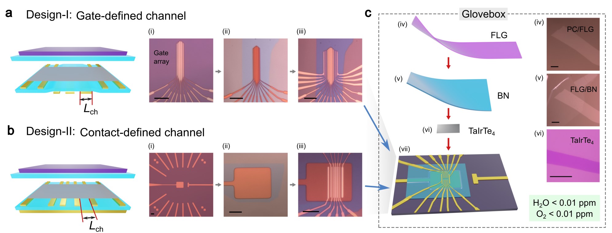
Mechanical exfoliation and layer number identification of TaIrTe4: The TaIrTe4 were exfoliated on Si/SiO2 substrates (SiO2 is 285 nm thickness) by the Scotch tape method. To address the air-sensitive nature of thin TaIrTe4 flakes, the exfoliation and the following device fabrication processes were performed in an argon-glovebox. We introduced gentle oxygen plasma treatment and heating process to increase the exfoliation yield. Prior to the exfoliation process, we employed a mild oxygen plasma treatment using the Anatech Barrel plasma cleaning system. The treatment involved a flow rate of 40 sccm at a power setting of 100 W for 10 minutes to clean the Si/SiO2 substrate. Subsequently, we placed the Si/SiO2 substrates onto the TaIrTe4 tape, carefully pressing the stack to eliminate any trapped air bubbles. The tape (with Si/SiO2 substrates) was then heated on a hot plate at a temperature of C for 10 minutes. Finally, we carefully removed the substrates from the TaIrTe4 tape and inspected them for the presence of thin flakes using an optical microscope.
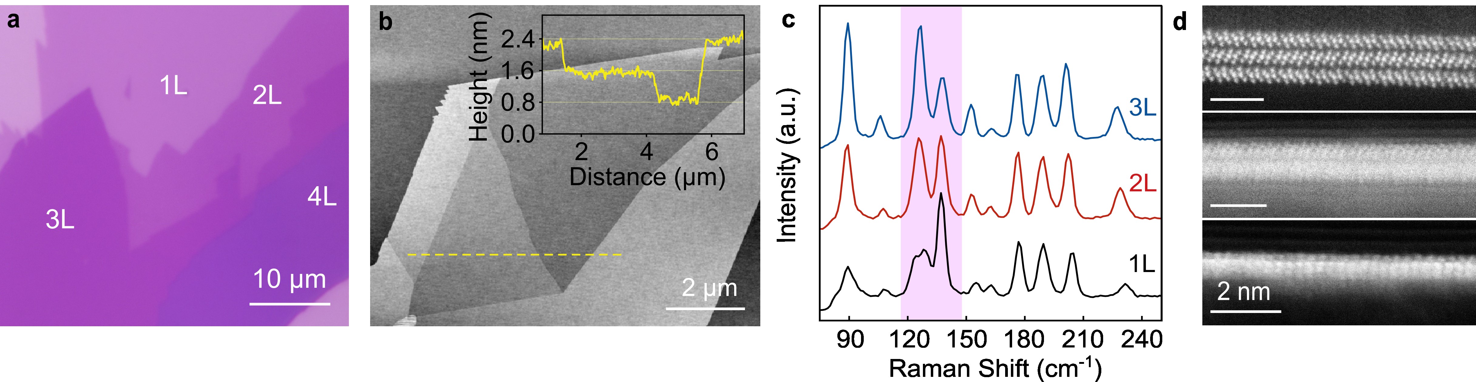
We used multiple characterizations to determine the layer number of TaIrTe4 flakes as shown in Extended Data Fig. 1, including optical contrast, atomic force microscopy (AFM), Raman spectroscopy, and cross-sectional STEM. Extended Data Fig. 1a displays optical images of representative TaIrTe4 flakes situated on a SiO2 substrate, revealing distinct optical contrast variations corresponding to different layer numbers. The quantitative relationship between optical contrast () and layer numbers can be found in SI 1.2. Extended Data Fig. 1b displays the surface morphology of exfoliated TaIrTe4 flakes, examined using a Park NX10 atomic force microscopy (AFM) system in tapping mode with a NCHR tip. The height linecut (inset) reveals a step of approximately 0.8 nm, indicative of a monolayer thickness. Raman spectroscopy also exhibits layer-dependent behavior (Extended Data Fig. 1c): with increasing layer numbers, the intensity ratio of A2 (@125.7 cm-1 for 1L)/A2 (@137.3 cm-1 for 1L) rises, and the A1 mode (@231.8 cm-1 for 1L) shifts toward lower wavenumbers. Additionally, cross-sectional STEM results in Extended Data Fig. 1d directly confirm the layer numbers (layer thickness approximately 0.7 nm, consistent with AFM results). These diverse characterization methods, collectively, and unambiguously determine layer numbers.
Device fabrication and measurements: Because of the air-sensitivity of thin TaIrTe4 flakes, we adopted the bottom contact structure with BN encapsulation. The metal electrodes (both gates and contacts) were patterned by standard UV or e-beam lithography via the Heidelberg PG101 laser writing and the Elionix HS50 e-beam writing systems. Metal electrodes, consisting of 2 nm Ti and 10 nm Pt layers, were deposited using an e-beam evaporator (Angstrom Engineering) and subsequently annealed in a tube furnace at C for 3 hours in an Ar/H2 (1:1) forming gas atmosphere. The metal electrodes were fabricated under ambient conditions and subsequently transferred into a glovebox for further processing. Within the glovebox, we conducted the assembly of the BN/few-layer graphene stack (for the top gate structure), as well as the exfoliation, identification, stacking, and encapsulation of TaIrTe4 flakes. This glovebox is equipped with a dry transfer stage and an optical microscope to facilitate these operations. For a detailed fabrication process, please refer to Extended Data Fig. 2 and SI 1.3. To safeguard the final device, we applied a PMMA capping layer via spin coating while still within the glovebox.
Electrical transport measurements were conducted using a variety of cryogenic systems, including the Montana cryostat, Quantum Design Opticool, PPMS, and MPMS3 systems. Standard lock-in techniques were predominantly employed to measure most of the electrical signals. Gate voltages were applied using Keithley source meters. In dual-gated devices, the charge carrier densities () and the external electric field () can be independently adjusted through the combination of the top gate voltage (Vtg) and the bottom gate voltage ().
| (1) |
| (2) |
Here, is the vacuum permittivity, is the BN dielectric constant () and is the thickness of the bottom (top) BN dielectric.
First-principles calculations: The electronic structures of TaIrTe4 were calculated from density functional theory via the Vienna ab-initio simulation package (VASP) [3]. The exchange correlation functional was considered by the generalized gradient approximation (GGA) [4]. The energy cutoff of plane waves was set to be eV and the smearing width of the Gaussian smearing method was chosen to be eV. A Gamma-centered mesh () was used for the BZ integrations. To get the ground state, the convergence criteria of lattice optimizations were set to 10-6 eV and 0.1 meV/ for the total energy and ionic forces, respectively. The optB88-vdW correlation functional [5] was used to describe the vdW interactions for 2D materials. The obtained Bloch wavefunctions were projected onto Wannier functions via using the WANNIER90 package [6]. The density functional perturbation theory implemented in VASP was performed to obtain the force constants with a supercell for phonon dispersion by Phonopy code [7]. The real space Hamiltonian was constructed by and orbitals of Ta, orbital of Te, and orbitals of Ir. The edge states were calculated by iterating the surface Green function [8]. The electronic susceptibility was calculated by the Lindhard function:
| (3) |
where is the Fermi Dirac distribution, is the momentum-dependence energy and is the broadening. The CDW modulation of electronic structure was performed by the Fröhlich-Peierls model [9]:
| (4) |
where is the modulation strength and only the intra-orbital interaction is considered. The periodicity of potential was determined by the vector denoted in Fig. 5d.
To figure out the origin of the topology of the band with superlattice potential, we perform calculations of bands and Wilson loop with continuously changed periodicity based on an eight-band tight-binding model. The eight-band tight-binding model is fitted by WANNIER90 package [6] and constructed by two Ta’s -orbital and two Te’s -orbital with spin-up, down components and spin-orbit coupling. We confirmed that our eight-band tight-binding model captures the same saddle points and helical edge as the tight-binding model with full orbitals.
Acknowledgements:
We thank Jennifer Cano, Valla Fatemi, Rafael Fernando, Luqiao Liu, Haizhou Lu, Xiao-Bin Qiang, Ying Ran, Brian Skinner, Aviram Uri, Ilija Zeljkovic, Fan Zhang, and Yi Zhang for fruitful discussions. Q.M. acknowledges the support by the AFOSR grant FA9550-22-1-0270 (transport measurements and data analysis). Q.M. and S.-Y.X. acknowledge the support from the Center for the Advancement of Topological Semimetals, an Energy Frontier Research Center funded by the US Department of Energy Office of Science, through the Ames Laboratory under contract DE-AC02-07CH11358 (device fabrication). Q.M. also acknowledges support from the NSF CAREER award DMR-2143426 (manuscript writing), the CIFAR global scholar program, and the Alfred P. Sloan Foundation. G.C. acknowledges the support from the National Research Foundation, Singapore under its Fellowship Award (NRF-NRFF13-2021-0010) and the Nanyang Assistant Professorship grant. N.N. acknowledges the supports from the US DOE, Office of Science, under Award Number DE-SC0021117 (single crystal growth and characterization of TaIrTe4). Y.S. acknowledges the support from the Strategic Priority Research Program of the Chinese Academy of Sciences (grants number XDB33030000) and the Informatization Plan of Chinese Academy of Sciences(CAS-WX2021SF-0102). K.S.B. and Y.W. acknowledges the support by the Air Force Office of Scientific Research under award number FA9550-20-1-0246. X.Q. acknowledges the support by the National Science Foundation (NSF) under Award Number DMR-1753054 and by the donors of ACS Petroleum Research Fund under grant number 65502-ND10. D.C.B. acknowledges the support from Harvard University Center for Nanoscale Systems, a member of the National Nanotechnology Coordinated Infrastructure Network, under NSF award number ECCS-2025158, and the STC Center for Integrated Quantum Materials, NSF grant number DMR-1231319. Z.S. acknowledges the support from Swiss National Science Foundation under grant number P500PT-206914. M.G. acknowledges the support of the National Science Foundation (NSF) EPMD program via grant 2211334. A.S. acknowledges the support by DMR-2103842. Portions of this research were conducted with the advanced computing resources provided by Texas A&M High Performance Research Computing. J. L. and Y. Z. are partly supported by the National Science Foundation Materials Research Science and Engineering Center program through the UT Knoxville Center for Advanced Materials and Manufacturing (Grant number DMR-2309083). L.F. and Q.M. acknowledge support from the National Science Foundation Convergence Program under grant number ITE-2235945. Ziqiang Wang is supported by the U.S. Department of Energy, Basic Energy Sciences grant number DE-FG02-99ER45747. K.W. and T.T. acknowledge support from the JSPS KAKENHI (Grant Numbers 21H05233 and 23H02052) and World Premier International Research Center Initiative (WPI), MEXT, Japan. We also acknowledge that some of the work was done in the Boston College cleanroom and nanotechnology facilities.
Author contributions: Q.M. conceived the experiments and supervised the project. J.T. fabricated the devices with the help of T.S.D., A.G., M.G., S.-Y.X., and K.S.B. J.T. performed the electrical measurements, and analyzed data with the assistance from T.S.D, A.G., Z.H., Z.S. M.S., V.B. and Z.H.W. A.S. and X.Q. performed the first-principles calculations of the single-particle band; H.C. and G.C. performed the calculations for different edge terminations, electronic susceptibility, CDW band structures, and topology; J.L. and Y.Z. performed the phonon dispersion calculation. L.F. and Z.Q.W. supplied the theory inputs. Y.W. and K.S.B. performed the Raman measurements. D.C.B. carried out the TEM characterization. T.Q., X.H., Y.S., and N.N. grew the TaIrTe4 bulk crystals. K.W. and T.T. grew the BN bulk crystals. Q.M., S.-Y.X., and J.T. wrote the manuscript with input from all authors.
Competing interests: The authors declare that they have no competing interests.
Data availability: Source data are available at https://doi.org/10.7910/DVN/JJAI19. All other data that support the plots within this paper and other findings of this study are available from the corresponding authors upon reasonable request.
References
- [1]
- [2]
- [3] Kresse, G. & Furthmüller, J. Efficient iterative schemes for ab initio total-energy calculations using a plane-wave basis set. Physical Review B 54, 11169 (1996).
- [4] Perdew, J. P., Burke, K. & Ernzerhof, M. Generalized gradient approximation made simple. Physical Review Letters 77, 3865 (1996).
- [5] Klimeš, J., Bowler, D. R. & Michaelides, A. Van der Waals density functionals applied to solids. Physical Review B 83, 195131 (2011).
- [6] Mostofi, A. A. et al. wannier90: A tool for obtaining maximally-localised Wannier functions. Computer Physics Communications 178, 685–699 (2008).
- [7] Togo, A. & Tanaka, I. First principles phonon calculations in materials science. Scripta Materialia 108, 1–5 (2015).
- [8] Bryant, G. W. Surface states of ternary semiconductor alloys: effect of alloy fluctuations in one-dimensional models with realistic atoms. Physical Review B 31, 5166 (1985).
- [9] Fröhlich, H. On the theory of superconductivity: The one-dimensional case. Proceedings of the Royal Society of London. Series A. Mathematical and Physical Sciences 223, 296–305 (1954).