Breakdown of the static dielectric screening approximation of Coulomb interactions in atomically thin semiconductors
Abstract
Coulomb interactions in atomically thin materials are uniquely sensitive to variations in the dielectric screening of the environment, which can be used to control quasiparticles and exotic quantum many-body phases. A static approximation of the dielectric response, where increased dielectric screening is predicted to cause an energy redshift of the exciton resonance, has been until now sufficient. Here, we use charge-tunable exciton resonances to study screening effects in transition metal dichalcogenide monolayers embedded in materials with dielectric constants ranging from to more than . In contrast to expectations, we observe a blueshift of the exciton resonance exceeding meV for larger dielectric constant environments. By employing a dynamical screening model, we find that while the exciton binding energy remains mostly controlled by the static dielectric response, the exciton self-energy is dominated by the high-frequency response. Dielectrics with markedly different static and high-frequency screening enable the selective addressing of distinct many-body effects in layered materials and their heterostructures, expanding the tunability range and offering new routes to detect and control correlated quantum many-body states and to design optoelectronic and quantum devices.
Introduction
Interactions amongst particles, or many-body effects, occupy a central role in physics. They give rise to collective phenomena described by new fundamental laws that arise when one ventures beyond simplified single-particle systems [1]. This is particularly evident in heterostructures of two-dimensional (D) materials, in which a wide variety of correlated electronic and excitonic phases have been realized, driven by strong Coulomb interactions [2, 3, 4, 5, 6]. For instance, excitonic complexes up to eight particles [7, 8, 9] and signatures of Wigner crystals [10] have recently been reported in encapsulated, gated monolayer transition metal dichalcogenides (TMDs). Hubbard physics [11, 12], unconventional superconductivity [13], and Chern insulators [14] have been observed in moiré superlattices.
In all such phenomena, Coulomb interactions are heavily influenced by the dielectric response of the environment because the electric field created by a quasiparticle in a 2D material extends into the surrounding medium [15, 16, 17, 18, 19]. Screening takes a central place in all field-matter interactions via susceptibility [20], affecting phase transitions of many-body states [21] and delimiting the range of charge interactions [22]. The response of a dielectric material to an electric field comes from its valence electrons and, if the material is polar, from field-induced lattice vibrations that induce a net polarization [23]. To describe screening in 2D materials, a common practice is to use an effective dielectric constant, neglecting frequency dependence [24, 25]. This approach greatly simplifies the description of interactions between quasiparticles and appeared so far sufficient to describe excitons in TMD monolayers [18, 26, 27, 28, 29, 30, 27].
Here, we unravel conditions under which the frequency-independent dielectric screening approximation breaks down, and dynamic effects become a key factor in determining excitonic behaviour. We track gate-tunable exciton resonances in monolayer WSe2 embedded in environments with static dielectric constants spanning three orders of magnitude but with a small range of high-frequency dielectric constants. In contrast with the preceding literature, we surprisingly observe an exciton resonance blueshift for larger static dielectric constants. We explain this behavior by showing that the exciton binding energy primarily responds to the static dielectric constant, while the self-energy primarily depends on the high-frequency dielectric constant. Our results reveal the necessity of including a dynamic description to fully capture screened many-body states in D systems. In addition, materials with strong frequency-dependent dielectric functions allow the selective tuning of exciton binding energy and self-energy, providing a knob to control quantum many-body states and their interactions and to design dielectric engineered optoelectronic and quantum devices.
Effect of the dielectric screening on the optical spectrum of monolayer TMDs
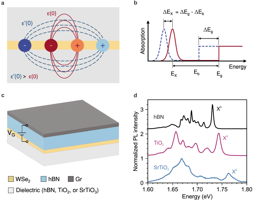
a, Schematic of an exciton and the electric field lines between its electron and hole when an atomically thin semiconductor is embedded in a weak (strong) screening environment whose effective dielectric constant is (). b, Sketches of the expected absorption spectra where denotes the energy resonance of the exciton ground state (n ), the binding energy, and the continuum bandgap energy (exciton energy in the limit n ). c, Schematic of our gate-tunable devices for the study of Coulomb interactions. In each device, a monolayer WSe2 is placed between hBN and a bottom dielectric, which is either hBN, TiO2, or SrTiO3. d, Normalized PL spectra of the different dielectric configurations at K. The resonance energy of the charge-neutral exciton X0 blueshifts with increasing static dielectric constant of the environment.
Figure 1a shows the schematic of an exciton in an atomically thin semiconductor embedded in environments with two different effective static dielectric constants and , where . Exciton states manifest as discrete optical resonances below the renormalized free-particle bandgap energy as shown in Fig. 1b for the exciton ground state. The dielectric environment affects the exciton resonance energy through changes to both its binding energy and self-energy, the latter being a bandgap renormalization (BGR) effect. For increasing effective dielectric constants, the quasiparticle self-energy reduces, inducing a redshift of the exciton resonance. At the same time, the exciton binding energy also decreases, thereby inducing a blueshift of the exciton resonance. The two effects are of the same order of magnitude in TMDs (up to hundreds of meV), almost cancelling each other [19, 26].
In the static approximation, the former is expected to be always slightly stronger than the latter by up to a few tens of meV [31, 25]. When calculating the BGR, the Coulomb potential is evaluated at a distance , whereas the binding energy is evaluated at a finite distance. Since the difference between the Coulomb potentials in two dielectric environments is greatest at , the net effect should always be a redshift of the exciton resonance with increasing static dielectric constant [31, 25]. Importantly, this picture also implies that static screening alone does not allow to independently tune binding energy and self-energy. To date, applications using dielectric engineering to control quasiparticles and their interactions, as well as to design devices, have rested on this understanding.
We fabricate charge-tunable devices based on monolayer WSe2 by using van der Waals fabrication techniques (Methods). In this study, we use WSe2 as a prototypical TMD material since it offers a larger exciton Bohr radius than Mo-based TMDs [32, 30], amplifying its sensitivity to the dielectric environment and because it does not display significant Fermi level pinning [7, 33]. Figure 1c shows the device configuration. Monolayer WSe2 is sandwiched between a top layer of hexagonal boron nitride (hBN) and a bottom dielectric with varying , either hBN, TiO2, or SrTiO3. Throughout this work, we will refer to the different dielectric configurations by their bottom dielectric layer. At temperatures K, the effective of these configurations range from for the hBN [10] sample, to for the TiO2 sample [34], and for the SrTiO3 sample [35]. Few-layer graphene (Gr) is used as a gate, allowing tuning of the electrochemical potential in all devices. Figure 1d shows the low-temperature photoluminescence (PL) spectra near charge neutrality, evidenced by the high ratio between neutral exciton X0 and negative trion X- intensities. In contrast to previous reports [28, 26, 29], the X0 energy surprisingly blueshifts with increasing effective dielectric constant, from eV in the hBN sample, to eV in the TiO2 sample, and further to eV in the SrTiO3 sample. These findings are not limited to WSe2, but we observe consistent blueshifts in monolayer MoSe2 and WS2 crystals embedded in the same dielectric environments (Supplementary Fig. ).
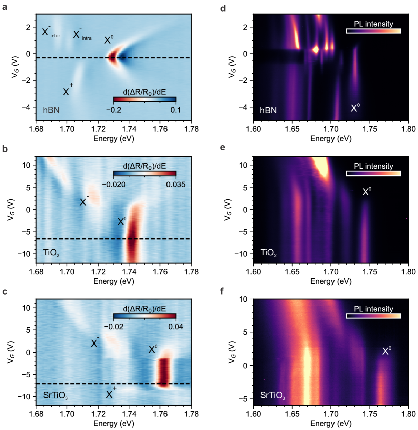
a-c, Gate-dependent reflection contrast derivative () of monolayer WSe2 in the hBN (a), TiO2 (b), and SrTiO3 (c) dielectric configuration. The voltage corresponding to charge neutrality is indicated by a dashed horizontal line. X0 and the charged excitons are labeled in the figures. At charge neutrality, X0 blueshifts with increasing effective static dielectric constant of the environment. d-f, Gate-dependent PL spectra of monolayer WSe2 in the hBN (d), TiO2 (e), and SrTiO3 (f) dielectric configuration. X0 is labeled in the figures.
To exclude a contribution to the exciton resonance shift from charge doping [36], we study the gate-dependent optical response of monolayer WSe2 in the different dielectric configurations. Figures 2a-c compare the gate-dependent reflection contrast derivatives () from the hBN, TiO2, and SrTiO3 samples. In all cases, we extract the X0 energy by fitting a dispersive Lorentzian at the charge neutrality point identified from the X0 absorption maximum (Supplementary Fig. ). In the hBN sample (Fig. 2a), the energy of X0 is eV. The spectrum of X0 exhibits a pronounced broadening and energy blueshift from charge neutrality to higher charge doping. This highlights the importance of evaluating excitonic energies at charge neutrality in such studies. The negative exchange-split trions [7] (X and X) appear in the electron-doped regime (positive ). In contrast, the positively charged trion [7] (X+) becomes visible in the hole-doped regime (negative ). The TiO2 sample (Fig. 2b) shows the X0 at eV, meV blueshifted with respect to X0 in the hBN sample. Even more, the SrTiO3 sample (Fig. 2c) shows a X0 energy of eV, meV blueshifted with respect to that in the hBN sample.
To further corroborate our findings, we inspect the optical response of WSe2 via gate-dependent PL spectroscopy, and extract the energy of X0 at charge neutrality. Figures 2d-f show the gate-dependent PL spectra of the hBN, TiO2, and SrTiO3 samples. In the hBN sample (Fig. 2d), the energy of X0 is eV, accompanied by a linewidth below meV, consistent with the highest quality samples reported in the literature [7, 33, 37, 38], and blueshifts due to charge doping by up to meV before disappearing (Supplementary Fig. ). The excited states , , , and are well-resolved in the PL spectra (Supplementary Fig. ), further testifying to the high sample quality [37, 38]. In the TiO2 sample (Fig. 2e), X0 has a linewidth of less than meV and appears at eV, blueshifted by meV compared to that in the hBN sample, which is consistent with the reflection contrast measurements. In the SrTiO3 sample (Fig. 2f), X0 has a linewidth of meV and arises at eV, blueshifted by meV compared to that in the hBN sample, once again in agreement with the reflection contrast data.
To exclude any contribution to the exciton energy shifts from uncontrolled strain fields [39] or other spatially dependent effects, we study the X0 energy distribution over large areas on multiple samples for each dielectric configuration (Supplementary Fig. ). We observe a narrow distribution below meV, reflecting the high homogeneity of the samples.
Having excluded these potential sources of blueshift, we conclude that X0 blueshifts with an increasing static dielectric constant of the environment. This implies that the corresponding reduction in the exciton binding energy must be greater than the BGR. Hence, the static approximation of Coulomb interactions is not sufficient to describe dielectric screening in atomically thin semiconductors.
Fully dynamical description of Coulomb screening
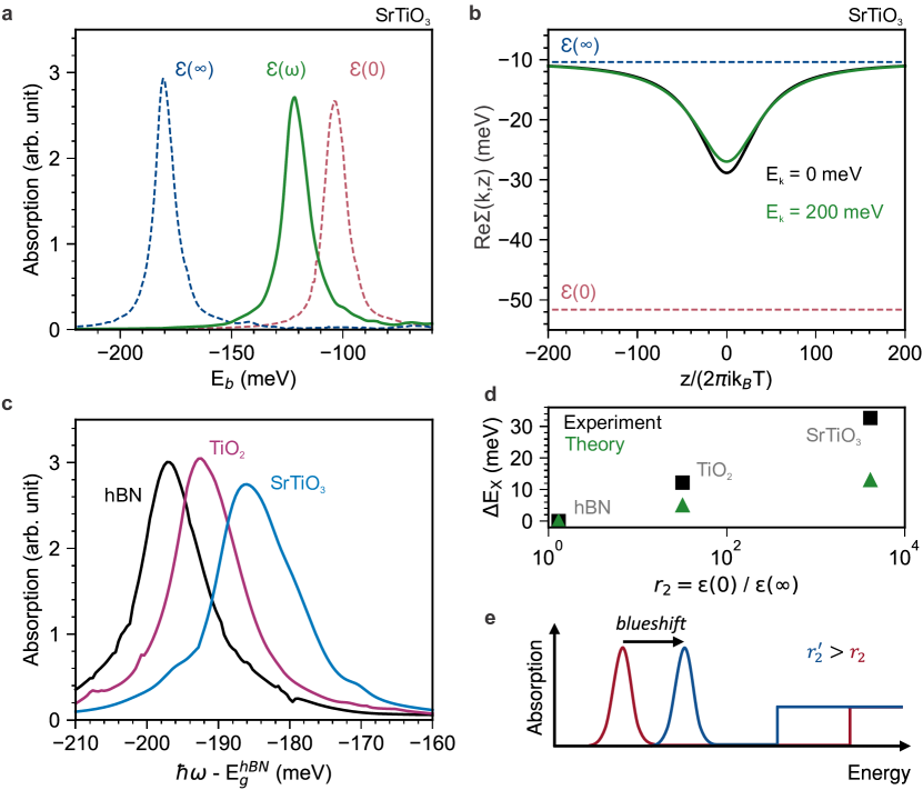
a, Calculated absorption spectrum of monolayer WSe2 on SrTiO3 without the BGR effect as a function of the exciton binding energy using (red), (blue), and (green). b, Calculated real part of the self-energy of conduction band electrons as a function of Matsubara frequencies for the SrTiO3 sample. Solid lines indicate dynamical calculations for two relevant electron energies, while dashed lines indicate static calculations. Zero energy is set to the calculated self-energy of the hBN sample for . c, Absorption spectra of the different samples obtained by combining binding energy and BGR calculated with dynamical screening (). The spectra are plotted relative to eV. d, Comparison of the energy shift as a function of the parameter from the optical experiments (black squares) and from the theoretical calculations (green arrows). e, Schematic of the absorption spectrum of a monolayer TMD highlighting the exciton resonance blueshift when increases from to .
To reconcile the contradiction between our results and the theory of screened many-body interactions, we turn to examining the role of frequency dependence in dielectric screening. The electron and hole are not independent entities; instead, they move with respect to each other with kinetic energy commensurate with the exciton binding energy as dictated by the virial theorem, resulting in a rapidly varying electric field [24, 31]. Consequently, we lift the assumption that the atoms of the encapsulating layers either perfectly trace or completely ignore the fast variation of the electric field. If the dielectric layer adjacent to the monolayer semiconductor is a polar material, we can approximate its response to electric field at frequency by the dielectric function:
The ratio between the static and high-frequency dielectric constants is the Lyddane–Sachs–Teller relation [23]. The index runs over the optical phonon modes, where is the associated frequency of the longitudinal/transverse optical lattice vibration in the dielectric layers. In the following, we use the formulation of the Coulomb potential designed for atomically thin semiconductors [24] and introduce dynamical dielectric functions to model the response of top and bottom dielectrics (Supplementary Theoretical Methods).
Figure 3a shows the calculated absorption spectrum of the SrTiO3 sample plotted in exciton binding energy units. The binding energy calculated with the static dielectric constant , which assumes that atoms can readily trace the varying electric field of the electron and hole, is meV smaller than that calculated with the high-frequency dielectric constant , which only considers the electronic contribution to the screening. Calculating the binding energy by using the dynamical dielectric function in the effective Bethe-Salpeter equation (BSE) [40], we obtain results closer to , indicating that the binding energy is mostly influenced by the static dielectric constant.
To include the dynamical effect, we calculate the self-energy of conduction band electrons from the solution of the Dyson equation [41]. Figure 3b shows the real part of the self-energy for the SrTiO3 sample as a function of imaginary Matsubara frequencies. The reference point at meV is set to the self-energy calculated for the hBN sample with . The self-energies calculated for the SrTiO3 sample at and are meV apart. We calculate the dynamical self-energy for two relevant electron energies of and meV. Across the whole Matsubara frequency spectrum, the self-energies remain close to the value calculated with , indicating that the dynamical self-energy is mainly influenced by the high-frequency dielectric constant.
Figure 3c presents the calculated absorption spectra of X0 by including the dynamics of both BGR and binding energy in the BSE for all the dielectric configurations considered in our experiments. The calculations show a net blueshift with increasing dielectric constant, in agreement with the experimental findings.
Figure 3d provides a comparison of the exciton resonance shift as a function of between the gate-dependent PL measurements and theory predictions. Despite the qualitative agreement, we note a lower calculated shift, possibly due to underestimation of the environmental screening in the model [24], as well as a possible smaller difference of the high-frequency dielectric constants (that is . Figure 3e summarizes the effect of dynamical screening on excitons when . X0 blueshifts because the binding energy blueshift contribution is larger than the BGR redshift contribution for a higher .
This finding stems from the dynamical dielectric screening. On the one hand, the BGR of a bound exciton is not the self-energy of a free electron in the conduction band plus that of a free hole in the valence band. In a bound pair, the bandgap energy introduces a relative phase between the electron and hole components, and therefore, at least one of these components is influenced by the high-frequency dielectric constant (Supplementary Theoretical Methods). On the other hand, the self-energy of a free charge particle is influenced by the static dielectric constant because the reference energy level in this case is the edge of the relevant energy band.
Our results are also consistent with works that utilized graphene as a screening layer for the Coulomb engineering of excitons in TMDs [29, 26]. Unlike in our case, where strongly polar oxides result in extremely high , the large carrier mobility in graphene results in a very effective electronic screening, which in turn leads to a low and redshifting X0 in TMDs. Crucially, our results indicate that the exciton self-energy and the exciton binding energy can be individually controlled by selecting screening materials with different values. Achieving the highest exciton energy difference at a dielectric heterojunction requires maximizing the between the different dielectric materials.
Effect of the dielectric screening on short-range Coulomb interactions
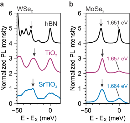
a, PL spectra of monolayer WSe2 on hBN, TiO2, and SrTiO3 in the electron doping regime. is taken as the origin of the energy axis. In WSe2, the negative trions are exchange-split. In each spectrum, X is indicated by a black arrow. b, PL spectra of monolayer MoSe2 on hBN, TiO2, and SrTiO3 in the electron doping regime. is taken as the origin of the energy axis, and it is indicated on the plots. X- is indicated by a black arrow in each spectrum.
To understand dielectric screening effects on many-body complexes beyond excitons, we also experimentally investigate the behavior of the trion. Figure 4a shows the PL spectra of monolayer WSe2 for the hBN, TiO2, and SrTiO3 samples in the electron doping regime, but close to charge neutrality (the X0 and negative trions intensities are comparable) to minimize energy shifts from charge doping. The exciton resonance X0 of each sample is taken as the origin of the energy axis to allow for a direct comparison of the trion binding energy across the different dielectric configurations. The negatively-charged intravalley trion X shows only a weak dependence on . Its binding energy starts at meV in the hBN sample, drops to meV in the TiO2 sample, and rises to meV in the SrTiO3 sample. The non-monotonic behavior may be attributed to residual energy shifts from inconsistencies in charge doping among samples. To investigate the same effect in a material with spectrally well-separated resonances, we also study the X- binding energy in monolayer MoSe2. Figure 4b shows the PL spectra of monolayer MoSe2 for the hBN, TiO2, and SrTiO3 samples in the electron doping regime. We first note that X0 in MoSe2 also experiences a blueshift of up to meV at higher values of . However, we do not observe any meaningful X- binding energy dependence on , with the change being of the order of only a few meV.
The weak sensitivity of the trion binding energy in WSe2 and MoSe2 to , together with the conservation of many of the excitonic features at extreme values, suggests that the formation of trions and other excitonic few-body complexes is only weakly affected by the static dielectric constant. At large distances, the interaction between a neutral exciton and an extra charge is dipolar in nature and, thus, has a relatively fast decay (). Consequently, the binding energy of few-body complexes such as the trion is governed by short-range interparticle interactions, which are not sensitive to static screening [24].
Conclusion
Exploring Coulomb interactions in atomically thin semiconductors beyond the static dielectric constant approximation breaks the monolithic picture of exciton binding energy change and BGR as effects governed by the same type of screening, revealing a more nuanced interplay of phenomena with distinct frequency dependence. Our results offer new avenues to study and manipulate many-body interactions. A natural consequence of our work would be to study the tuning of interlayer and moiré excitons via the dielectric environment. Using excitonic resonances as sensors for charge ordering could now provide deeper insights into correlated states. An exciting direction would be to explore the tuning of long-range interactions in strongly correlated systems, for example, in systems realizing the extended Hubbard model. This may allow the realization of currently inaccessible many-body phases, including interaction-induced Chern insulators and quantum spin liquids [42, 43]. Finally, enabling the deterministic fabrication of dielectric superlattices could unlock the study of strongly correlated physics in artificial solid-state crystals and quasicrystals [44].
Methods
Sample preparation
All TMD and hBN flakes were mechanically exfoliated from bulk crystals on SiO2 substrates. The flakes were selected based on their optical contrast, shape, and cleanliness. The devices were assembled via the dry-transfer technique using polycarbonate films [45] for the hBN and TiO2 devices and using polypropylene carbonate [46] for the SrTiO3 devices. Contacts to the respective layers were patterned using optical lithography and electron beam evaporation Cr/Au nm. Single-crystal substrates of TiO2 and SrTiO3 were acquired from Shinkosha Co., Ltd.
Optical spectroscopy
The optical measurements were performed in a variable-temperature helium flow cryostat with a confocal microscope in reflection geometry. For the PL measurements, nm / nm continuous wave laser sources were used for the excitation. The laser beam was focused onto the sample using an objective with a numerical aperture of , yielding an excitation spot size of around m. A pinhole was used as a spatial filter to obtain a diffraction-limited collection spot. The collected light is dispersed using a grating monochromator and detected on a CCD sensor array. The laser light was filtered using a nm short-pass filter. For reflection spectroscopy, thermal light from a tungsten halogen light source was used for excitation. The gate voltage in the gate-tunable measurements was controlled using a Keithley source meter.
Data availability
The datasets generated and analyzed during the current study are available from the corresponding authors upon reasonable request.
References
- Snoke [2019] D. W. Snoke, Solid State Physics: Essential Concepts, 2nd ed. (Cambridge University Press, Cambridge, United Kingdom ; New York, NY, 2019).
- Yankowitz et al. [2019] M. Yankowitz, Q. Ma, P. Jarillo-Herrero, and B. J. LeRoy, Nature Reviews Physics 1, 112 (2019).
- Mak and Shan [2022] K. F. Mak and J. Shan, Nature Nanotechnology 17, 686 (2022).
- Wilson et al. [2021] N. P. Wilson, W. Yao, J. Shan, and X. Xu, Nature 599, 383 (2021).
- Regan et al. [2022] E. C. Regan, D. Wang, E. Y. Paik, Y. Zeng, L. Zhang, J. Zhu, A. H. MacDonald, H. Deng, and F. Wang, Nature Reviews Materials 7, 778 (2022).
- Montblanch et al. [2023] A. R.-P. Montblanch, M. Barbone, I. Aharonovich, M. Atatüre, and A. C. Ferrari, Nature Nanotechnology 18, 555 (2023).
- Barbone et al. [2018] M. Barbone, A. R.-P. Montblanch, D. M. Kara, C. Palacios-Berraquero, A. R. Cadore, D. De Fazio, B. Pingault, E. Mostaani, H. Li, B. Chen, K. Watanabe, T. Taniguchi, S. Tongay, G. Wang, A. C. Ferrari, and M. Atatüre, Nature Communications 9, 3721 (2018).
- Sidler et al. [2017] M. Sidler, P. Back, O. Cotlet, A. Srivastava, T. Fink, M. Kroner, E. Demler, and A. Imamoglu, Nature Physics 13, 255 (2017).
- Van Tuan et al. [2022] D. Van Tuan, S.-F. Shi, X. Xu, S. A. Crooker, and H. Dery, Physical Review Letters 129, 076801 (2022).
- Smoleński et al. [2021] T. Smoleński, P. E. Dolgirev, C. Kuhlenkamp, A. Popert, Y. Shimazaki, P. Back, X. Lu, M. Kroner, K. Watanabe, T. Taniguchi, I. Esterlis, E. Demler, and A. Imamoğlu, Nature 595, 53 (2021).
- Tang et al. [2020] Y. Tang, L. Li, T. Li, Y. Xu, S. Liu, K. Barmak, K. Watanabe, T. Taniguchi, A. H. MacDonald, J. Shan, and K. F. Mak, Nature 579, 353 (2020).
- Xu et al. [2020] Y. Xu, S. Liu, D. A. Rhodes, K. Watanabe, T. Taniguchi, J. Hone, V. Elser, K. F. Mak, and J. Shan, Nature 587, 214 (2020).
- Cao et al. [2018] Y. Cao, V. Fatemi, S. Fang, K. Watanabe, T. Taniguchi, E. Kaxiras, and P. Jarillo-Herrero, Nature 556, 43 (2018).
- Chen et al. [2020] G. Chen, A. L. Sharpe, E. J. Fox, Y.-H. Zhang, S. Wang, L. Jiang, B. Lyu, H. Li, K. Watanabe, T. Taniguchi, Z. Shi, T. Senthil, D. Goldhaber-Gordon, Y. Zhang, and F. Wang, Nature 579, 56 (2020).
- Rytova [2020] N. S. Rytova, Screened potential of a point charge in a thin film (2020), arxiv:1806.00976 .
- Keldysh [1979] L. V. Keldysh, JETP Letters 29, 658 (1979).
- Cudazzo et al. [2011] P. Cudazzo, I. V. Tokatly, and A. Rubio, Physical Review B 84, 085406 (2011).
- Chernikov et al. [2014] A. Chernikov, T. C. Berkelbach, H. M. Hill, A. Rigosi, Y. Li, B. Aslan, D. R. Reichman, M. S. Hybertsen, and T. F. Heinz, Physical Review Letters 113, 076802 (2014).
- Ugeda et al. [2014] M. M. Ugeda, A. J. Bradley, S.-F. Shi, F. H. da Jornada, Y. Zhang, D. Y. Qiu, W. Ruan, S.-K. Mo, Z. Hussain, Z.-X. Shen, F. Wang, S. G. Louie, and M. F. Crommie, Nature Materials 13, 1091 (2014).
- Petrić et al. [2023] M. M. Petrić, V. Villafañe, P. Herrmann, A. Ben Mhenni, Y. Qin, Y. Sayyad, Y. Shen, S. Tongay, K. Müller, G. Soavi, J. J. Finley, and M. Barbone, Advanced Optical Materials 11, 2300958 (2023).
- Fogler et al. [2014] M. M. Fogler, L. V. Butov, and K. S. Novoselov, Nature Communications 5, 4555 (2014).
- Knörzer et al. [2022] J. Knörzer, C. J. van Diepen, T.-K. Hsiao, G. Giedke, U. Mukhopadhyay, C. Reichl, W. Wegscheider, J. I. Cirac, and L. M. K. Vandersypen, Physical Review Research 4, 033043 (2022).
- Lyddane et al. [1941] R. H. Lyddane, R. G. Sachs, and E. Teller, Physical Review 59, 673 (1941).
- Van Tuan et al. [2018] D. Van Tuan, M. Yang, and H. Dery, Physical Review B 98, 125308 (2018).
- Cho and Berkelbach [2018] Y. Cho and T. C. Berkelbach, Physical Review B 97, 041409 (2018).
- Raja et al. [2017] A. Raja, A. Chaves, J. Yu, G. Arefe, H. M. Hill, A. F. Rigosi, T. C. Berkelbach, P. Nagler, C. Schüller, T. Korn, C. Nuckolls, J. Hone, L. E. Brus, T. F. Heinz, D. R. Reichman, and A. Chernikov, Nature Communications 8, 15251 (2017).
- Raja et al. [2019] A. Raja, L. Waldecker, J. Zipfel, Y. Cho, S. Brem, J. D. Ziegler, M. Kulig, T. Taniguchi, K. Watanabe, E. Malic, T. F. Heinz, T. C. Berkelbach, and A. Chernikov, Nature Nanotechnology 14, 832 (2019).
- Stier et al. [2016] A. V. Stier, N. P. Wilson, G. Clark, X. Xu, and S. A. Crooker, Nano Letters 16, 7054 (2016).
- Tebbe et al. [2023] D. Tebbe, M. Schütte, K. Watanabe, T. Taniguchi, C. Stampfer, B. Beschoten, and L. Waldecker, npj 2D Materials and Applications 7, 1 (2023).
- Goryca et al. [2019] M. Goryca, J. Li, A. V. Stier, T. Taniguchi, K. Watanabe, E. Courtade, S. Shree, C. Robert, B. Urbaszek, X. Marie, and S. A. Crooker, Nature Communications 10, 4172 (2019).
- Scharf et al. [2019] B. Scharf, D. V. Tuan, I. Žutić, and H. Dery, Journal of Physics: Condensed Matter 31, 203001 (2019).
- Stier et al. [2018] A. V. Stier, N. P. Wilson, K. A. Velizhanin, J. Kono, X. Xu, and S. A. Crooker, Physical Review Letters 120, 057405 (2018).
- He et al. [2020] M. He, P. Rivera, D. Van Tuan, N. P. Wilson, M. Yang, T. Taniguchi, K. Watanabe, J. Yan, D. G. Mandrus, H. Yu, H. Dery, W. Yao, and X. Xu, Nature Communications 11, 618 (2020).
- Schöche et al. [2013] S. Schöche, T. Hofmann, R. Korlacki, T. E. Tiwald, and M. Schubert, Journal of Applied Physics 113, 164102 (2013).
- Neville et al. [1972] R. C. Neville, B. Hoeneisen, and C. A. Mead, Journal of Applied Physics 43, 2124 (1972).
- Van Tuan et al. [2019] D. Van Tuan, B. Scharf, Z. Wang, J. Shan, K. F. Mak, I. Žutić, and H. Dery, Physical Review B 99, 085301 (2019).
- Liu et al. [2019] E. Liu, J. van Baren, T. Taniguchi, K. Watanabe, Y.-C. Chang, and C. H. Lui, Physical Review B 99, 205420 (2019).
- Liu et al. [2021] E. Liu, J. van Baren, Z. Lu, T. Taniguchi, K. Watanabe, D. Smirnov, Y.-C. Chang, and C. H. Lui, Nature Communications 12, 6131 (2021).
- Aslan et al. [2018] B. Aslan, M. Deng, and T. F. Heinz, Physical Review B 98, 115308 (2018).
- Salpeter and Bethe [1951] E. E. Salpeter and H. A. Bethe, Physical Review 84, 1232 (1951).
- Dyson [1949] F. J. Dyson, Physical Review 75, 1736 (1949).
- Wu et al. [2018] F. Wu, T. Lovorn, E. Tutuc, and A. H. MacDonald, Physical Review Letters 121, 026402 (2018).
- Pan et al. [2020] H. Pan, F. Wu, and S. Das Sarma, Physical Review B 102, 201104 (2020).
- Forsythe et al. [2018] C. Forsythe, X. Zhou, K. Watanabe, T. Taniguchi, A. Pasupathy, P. Moon, M. Koshino, P. Kim, and C. R. Dean, Nature Nanotechnology 13, 566 (2018).
- Purdie et al. [2018] D. G. Purdie, N. M. Pugno, T. Taniguchi, K. Watanabe, A. C. Ferrari, and A. Lombardo, Nature Communications 9, 5387 (2018).
- Wang et al. [2013] L. Wang, I. Meric, P. Y. Huang, Q. Gao, Y. Gao, H. Tran, T. Taniguchi, K. Watanabe, L. M. Campos, D. A. Muller, J. Guo, P. Kim, J. Hone, K. L. Shepard, and C. R. Dean, Science 342, 614 (2013).
Acknowledgments
We thank Eduardo Zubizarreta-Casalengua and Ferdinand Menzel for useful discussions. A.B.M acknowledges funding from the International Max Planck Research School for Quantum Science and Technology (IMPRS-QST). M.B. acknowledges funding from the A. von Humboldt Foundation. We gratefully acknowledge funding from the Deutsche Forschungsgemeinschaft (DFG, German Research Foundation) via Germany’s Excellence Strategy (MCQST, EXC-2111/390814868, and e-conversion, EXC-2089/1-390776260). J.J.F. also acknowledges the BMBF for funding via projects 16K15Q027, 13N15760, 13N16214, as well as the DFG via INST 95/1719-1, FI 947/6-1, INST 95/1496-1, FI 947/5-1, FI 947/8-1, DI 2013/5-1 and DI 2013/5-2. K.M. also acknowledges the DFG via the project PQET (INST 95/1654-1). Furthermore, we acknowledge the Bavarian Science Ministry for funding via the Munich Quantum Valley, Nequs, and IQ-Sense projects. Work at the University of Rochester was supported by the Department of Energy, Basic Energy Sciences, Division of Materials Sciences and Engineering under Award No. DE-SC0014349. S.T. acknowledges primary support from DOE-SC0020653 (materials synthesis), NSF CMMI 1825594 (NMR and TEM studies), NSF ECCS 2052527 (electrical testing), DMR 2111812 (optical testing), and CMMI 2129412 (scaling). K.W. and T.T. acknowledge support from the JSPS KAKENHI (Grant Numbers 20H00354 and 23H02052) and World Premier International Research Center Initiative (WPI), MEXT, Japan.
Author contributions
A.B.M. and M.B. conceived and managed the research. A.B.M., and L.G. prepared the samples. A.B.M., L.G., M.M.P., and M.B. performed the optical measurements. A.B.M. and M.B. analyzed the results. J.J.F. and K.M. obtained third party funding and provided experimental and nanofabrication infrastructure. D.V.T. and H.D. developed the models and performed the calculations. M.E. and S.T. grew WSe2, WS2, and MoSe2 bulk crystals. K.W. and T.T. grew bulk hBN crystals. All authors discussed the results and contributed to the writing of the paper.
Competing interests
The authors declare no competing interests.
Supplementary information
Theoretical Methods and Supplementary Figs. 1–5.