A 4 - 8 GHz Kinetic Inductance Travelling-Wave Parametric Amplifier Using Four-Wave Mixing with Near Quantum-Limit Noise Performance
Abstract
Kinetic inductance traveling-wave parametric amplifiers (KI-TWPA) have a wide instantaneous bandwidth with near quantum-limited sensitivity and a relatively high dynamic range. Because of this, they are suitable readout devices for cryogenic detectors and superconducting qubits and have a variety of applications in quantum sensing. This work discusses the design, fabrication, and performance of a KI-TWPA based on four-wave mixing in a NbTiN microstrip transmission line. This device amplifies a signal band from 4 to 8 GHz without contamination from image tones, which are produced in a separate higher frequency band. The 4 - 8 GHz band is commonly used to read out cryogenic detectors, such as microwave kinetic inductance detectors (MKIDs) and Josephson junction-based qubits. We report a measured maximum gain of over 20 dB using four-wave mixing with a 1-dB gain compression point of -58 dBm at 15 dB of gain over that band. The bandwidth and peak gain are tunable by adjusting the pump-tone frequency and power. Using a Y-factor method, we measure an amplifier-added noise of photons from 4.5 - 8 GHz.
I Introduction
Using a quantum noise-limited parametric amplifier as a first-stage amplifier for readout can improve the sensitivity of multiple cryogenic detector technologies, such as the Microwave Kinetic Inductance Detector (MKID) Zobrist et al. (2019), , and microwave SQUID multiplexer (MUX) readout of Mettalic Magnetic Calorimeters Kempf et al. (2017) and Transition-Edge Sensors Malnou et al. (2023a). Traveling wave parametric amplifiers are also an appealing choice for fast and high-fidelity readout Peng et al. (2022); Barzanjeh, DiVincenzo, and Terhal (2014); Didier et al. (2015) of cryogenic qubits. A commonly used frequency band to read out superconducting qubits and detectors is 4 - 8 GHz due to its availability, accessibility, and maturity of readout electronic systems and components at a relatively low cost. Applications of superconducting parametric amplifiers also extend to fundamental physics research for laboratory-based experiments such as dark matter searches, where a quantum-noise-limited gain is of interest Ramanathan et al. (2023).
The resonant Josephson junction amplifiers (JPAs) are the most commonly used superconducting parametric amplifiers Aumentado (2020). Even though these devices have shown quantum-limited noise performance, they have low fractional bandwidths and very low dynamic rangeEsposito et al. (2021). Recently, by implementing a traveling-wave periodic structureAumentado (2020); Mutus et al. (2013), the bandwidths of Josephson traveling-wave parametric amplifiers (JTWPAs) have been increased to a few gigahertz Macklin et al. (2015). However, the low dynamic range of these devices still remains an issue, especially for the readout of resonator arrays Mutus et al. (2013). In addition, the complexity of circuitry of the nonlinear lumped element transmission line and junction fabrication also puts them at a disadvantage compared to their counterparts, the kinetic inductance-based parametric amplifiersShu et al. (2021); Malnou et al. (2021); Eom et al. (2012); Ranzani et al. (2018); Vissers et al. (2016); Chaudhuri et al. (2017); Shan, Sekimoto, and Noguchi (2016); Boc (2014).
Kinetic inductance-based superconducting parametric amplifiers utilize the nonlinear kinetic inductance of superconducting thin films such as NbTiN. Four-wave mixing (4WM) processes can occur in kinetic inductance transmission line structures patterned in coplanar waveguide Eom et al. (2012) or microstrip line Shu et al. (2021) geometries when a strong pump tone is present. To obtain maximum gain over a desired bandwidth, a phase-matching condition is necessary. Implementing geometric dispersion allows for control of phase matching. This technique, called dispersion engineering, can also be utilized to mismatch unwanted higher-order nonlinear processes such as pump third harmonicEom et al. (2012).
Three-wave mixing (3WM) is possible with KI-TWPAs when a constant current is applied to the transmission line. 3WM KI-TWPAs have demonstrated a near quantum-limited noise, wide bandwidth, and high dynamic rangeKlimovich (2022); Malnou et al. (2021). However, since the pump tone corresponds to twice the frequency at the center of the gain curve, it is then folded about its center in the sense that a signal on one side of produces an idler tone at the reflected frequency of . That situation is far from ideal for reading out densely frequency-spaced arrays of resonators where the resulting frequency collisions would seriously impact the yield and other cases where there is power at frequencies corresponding to the idler part of the band. The total bandwidth of the published 3WM devices is also somewhat less than 4-8 GHz Klimovich (2022); Malnou et al. (2021).
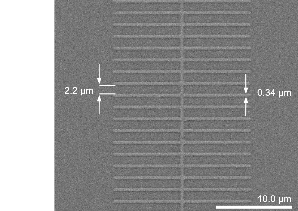
This paper presents a four-wave mixing KI-TWPA, where the pump tone is between the signal and idler frequencies, . The amplifier tends to produce a gain in disjointed frequency ranges that we will refer to as the signal and idler (or image) bands, which makes it possible to separate the idler using ancillary circuitry and use the full signal band without contamination from the image (or idler) frequencies. The devices described here are made of NbTiN and patterned in an inverted microstrip geometryShu et al. (2021). The transmission line is dispersion engineered by adding sinusoidally modulated capacitive stubs with a median length of 9.2 and modulation of 2.08 to create a bandgap centered at 12.5 GHz.
II Device Design and Fabrication
The design of the device is similar to what was reported in Shu et al. Shu et al. (2021) with the exception of Nb as the ground plane. To effectively increase the nonlinearity in the kinetic inductance of the transmission line as a function of the pump current (), the transmission line width was designed to be 320 nm as shown in Fig. 1.a. The kinetic inductance per unit length as a function of pump current is given by the following relationEom et al. (2012):
| (1) |
where is the “characteristic” current that sets the scale of the nonlinearity.
The increase in the impedance of the transmission line, , due to its narrow width and large kinetic inductance was compensated for by adding capacitive stubs to increase the capacitance per unit length,, of the transmission line. The length of the stubs was set to create the dispersion needed for the four-wave mixing process and further modulated along the length of the transmission line to create a photonic bandgap Eom et al. (2012) around the pump frequency, as shown in Fig 1.b.
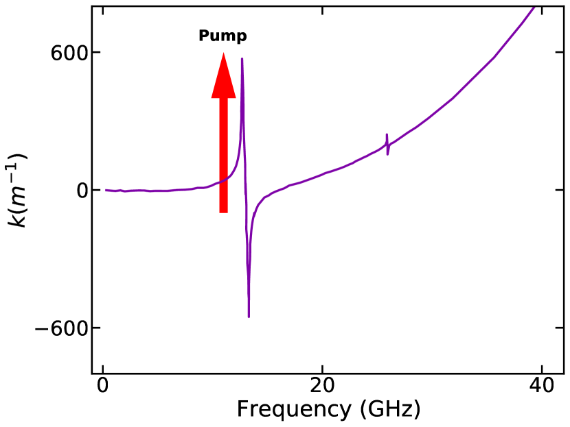
We can approach the following phase-matching criterion for a wide range of frequencies by putting the pump at the upward step before the bandgap:
| (2) |
where ,, and are the wave vectors corresponding to the signal, idler, and pump tones, respectively, and the term on the right represents the nonlinear dispersive effect Eom et al. (2012).Fig. 1.c shows a plot of as a function of frequency.
The devices were fabricated by depositing a 35-nm thick NbTiN layer on a 6-inch high resistivity () silicon wafer via reactive sputtering from a NbTi target in a nitrogen atmosphere at ambient temperatures. The NbTiN film was then patterned using a stepper photo-lithography method, and then etched in a reactive ion etcher. Utilizing a Plasma-Enhanced Chemical Vapor Deposition (PECVD) process, a 60-nm thick amorphous silicon layer was deposited on top of the NbTiN wire. Finally, a 350-nm thick Nb ground-plane layer was sputtered on top of the amorphous silicon layer and then patterned and etched.
III Results and Discussion
III.1 Behavior
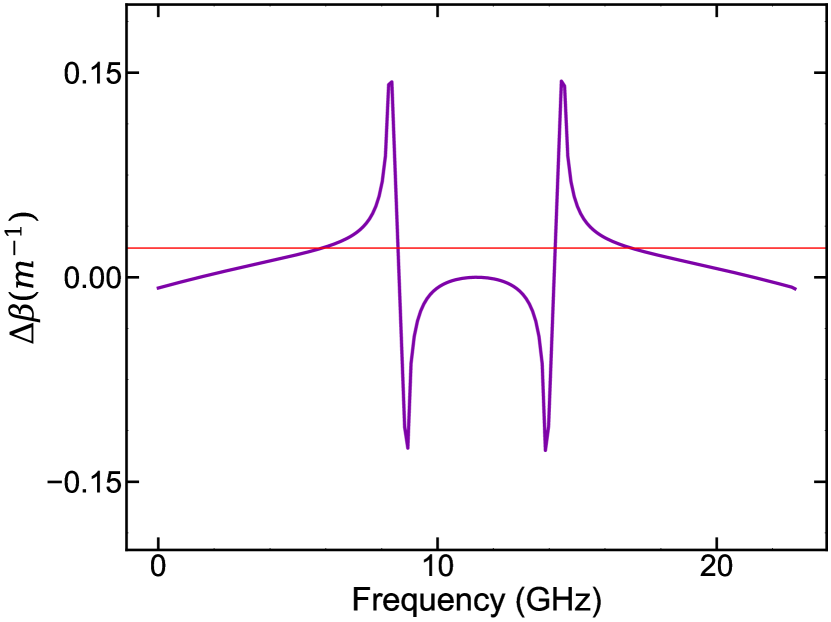
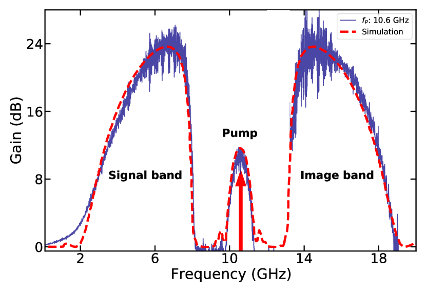
The gain is measured by normalizing the pumped transmission by the pump-off transmission. We expect negligible loss from the KI-TWPA based on results reported in Shu et al.Shu et al. (2021) for a similar device geometry in this frequency range. The KI-TWPA tends to produce gain in disjointed frequency ranges that we refer to as the signal and idler bands (see Fig. 1.a). The amplifier also produces some gain in a narrow frequency band around the pump frequency, but the gain there is less because, in that frequency range, the nonlinear dispersive effect is not compensated by the engineered dispersion. The gap in the gain curve around 12.5 GHz is simply the result of the transmission gap due to the modulation of the stub lengths. The additional gap around 8.7 GHz occurs because with the signal tone near that frequency, the idler tone would fall within the bandgap, and therefore, the gain process is inoperative. The gaps in the gain curve serve a useful function in that it is easier to use a diplexer to separate out the pump and the signal and idler bands. Typically, diplexers have poor input matching at their crossover frequencies, so by placing those frequencies in the zero gain regions, potential problems with reflections can be avoided.
To plot the expected gain of the device, we extracted the phase velocity of the KI-TWPA by fitting its unpumped transmission to the network model of the KI-TWPA non-linear transmission line. To achieve a similar gain level to the measured value, we adjusted the value of the pump current in the coupled-mode equationsShu et al. (2021). Comparing the simulation plot shown in Fig. 2.a indicates a good agreement with measurement results plotted in the same figure.If we adjust the frequency of the pump tone to different levels below the bandgap, it is possible to achieve phase matching of the signal and idler tones depending on the dispersion at the pump at those frequencies. The relationship between the signal, idler, and pump tones in four-wave mixing can be expressed as follows
| (3) |
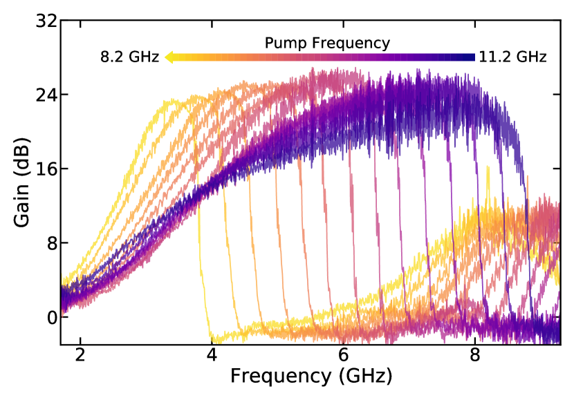
where , , and are the signal, pump, and idler frequencies, respectively. Fig. 2.b shows the signal band gain for different pump tone frequencies measured at 1 K.
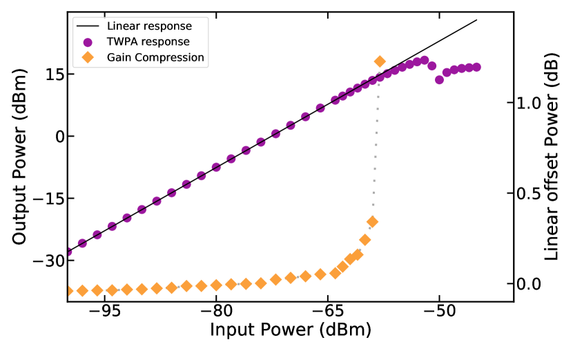
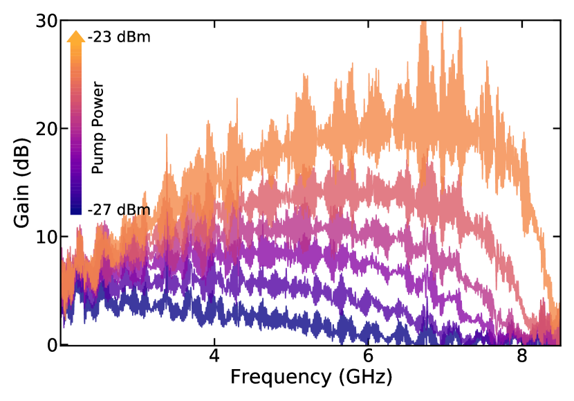
To measure the compression point, a test tone in the middle of the device’s signal band was injected into the KI-TWPA, and the system’s output power was measured using a spectrum analyzer. With the pump frequency set to 10.6 GHz and pump tone power of -23 dBm, resulting in 15 dB of gain, the output power of the amplified test tone at the spectrum analyzer was measured as a function of the test tone’s power at the device. As shown in Fig. 3.a, the gain compresses by 1 dB when the input signal at the device is -58 dBm. Since the compression point of the KI-TWPA is set by the pump depletion effect, the pump is depleted when the output power of the KI-TWPA reaches -43 dBm in this case.
III.2 Noise
The amplifier chain noise was measured using a Y-factor method with two 50 cryogenic loads as noise sources, one at 3.18 K and the other at the Mixing Chamber (MXC) stage ( 20 mK) of the dilution refrigerator. Using a cryogenic relay switch, we alternate between the noise sources as shown in Fig. 4.a. Due to a lack of output-to-input isolation, reflections must be avoided at either side of the TWPA at frequencies where the amplifier has gain. If the sum of the dB return losses on the input and output sides does not exceed the gain, an oscillation will develop. The circuit shown in Fig. 4 achieves this using a combination of diplexer (DPX) circuits. The input side diplexers allow for the injection of the pump tone through a bandpass filter (not shown) that removes synthesizer phase noise. The input side DPX I provides a cold termination to the input of the KI-TWPA over the idler band (13 GHz). The noise from that termination determines the added noise of the KI-TWPA, so it is kept at a temperature mK for the system to be quantum limited. In this configuration, the KI-TWPA only receives the thermal noise emitted from the calibration sources in the signal band.
On the output side of the KI-TWPA, the diplexer removes the pump and idler tones and terminates them. The pump is terminated at a higher temperature stage ( 50 mK) to minimize heating. The idler is terminated at the base temperature to avoid noise from that termination, which may travel back through the KI-TWPA from output to input and possibly be reflected back into the KI-TWPA. Finally, an isolator is used to avoid noise from the HEMT, which may otherwise contaminate the KI-TWPA via the same mechanism. the noise spectrum is then read through a room-temperature low noise amplifier (LNA) and measured using a spectrum analyzer.
The total system noise spectrum in units of quanta, which includes the KI-TWPA, a Low Noise Factory cryogenic HEMT amplifier (Model: LNF-LNC0.3_14B), and a room temperature low noise amplifier, was measured using the Y-factor method,
| (4) |
where is the signal angular frequency, is the Boltzmann constant, and is the reduced Planck’s constant. The and are the effective temperatures of the hot and cold terminations given by Kerr and Feldman (1996)
| (5) |
where is the physical temperature of the noise sources.
The KI-TWPA added noise was measured using the gain of the KI-TWPA and the total system noise. However, microwave losses in the measurement setup, especially between the KI-TWPA and the noise sources, can cause an overestimation of the measured noise. We estimated the loss from the diplexers by comparing the measured transmission through the KI-TWPA and diplexers to a cable bypassing them. After considering the loss, the added noise of the KI-TWPA can be calculated using the following equation.
| (6) | ||||
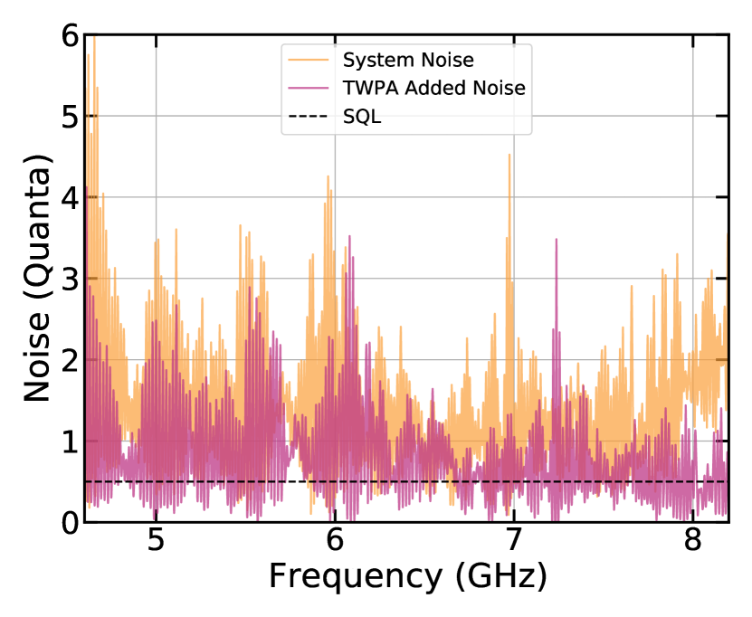
where is the added noise of the KI-TWPA, and are the losses in components before and after the KI-TWPA, respectively. is the quantum noise, is the added noise of the HEMT amplifier and is the measured gain of the KI-TWPA. The noise model used to arrive at equation (6) is explained in Appendix B. We measure a total system noise of in the 4.6 - 8.1 GHz range. Using equation (6), we estimate the added noise of the KI-TWPA to be as shown in Fig. 4. We can also estimate the cryogenic HEMT amplifier’s noise from unpumped KI-TWPA measurements, where we measure an average noise temperature of 5 K or 13 quanta in the 4 - 8 GHZ band consistent with data provided in the amplifier’s datasheet. It was observed that fluctuations in the measured noise spectra and added noise in TWPA were more than half a quanta. These fluctuations could be attributed to some nonidealities in the test setup that could be improved. For instance, both noise sources are connected to the input of the KI-TWPA through three cables and two switches. Estimating the insertion loss in all these components is quite challenging, and any unaccounted losses can lead to uncertainty in the measurement and overestimation of the measured noise. To address this issue, we can use a Variable Temperature Source (VTS) or a shut-noise tunnel junction (SNTJ) Malnou et al. (2023b). Using a VTS would require only one 50 termination and could be physically placed closer to the KI-TWPA. This could lead to fewer cables required between the noise source and KI-TWPA, which would improve the uncertainty and loss of the noise power at the input of the KI-TWPA.
IV Conclusion
In conclusion, we have designed, fabricated, and measured a wide-bandwidth Four-Wave Mixing KI-TWPA that produces gain between 3 - 9 GHz with a 1 dB compression of -58 dBm suitable for the readout of large detector arrays and superconducting qubits. We have demonstrated a near quantum-limited noise performance of KI-TWPA in the 4.5 to 8 GHz frequency range using a y-factor method.
The signal band peak gain of this device is shown to be tunable with the frequency of the pump tone. This tunability makes the KI-TWPA very robust for applications where the signal gain needs to be adjusted, such as in dark matter experiments. Moving forward, KI-TWPA performance could benefit from using lower materials with high kinetic inductance. For instance, a KI-TWPA with a TiN or WSi signal layer would require lower pump power to achieve parametric gain. We also intend to design and integrate superconducting diplexer circuits with the KI-TWPA for compactness and robustness.
Acknowledgements.
This research was carried out at the Jet Propulsion Laboratory under a contract with the National Aeronautics and Space Administration (80NM0018D0004). F.F’s research was supported by appointment to the NASA Postdoctoral Program at the Jet Propulsion Laboratory, administered by Oak Ridge Associated Universities under contract with NASA.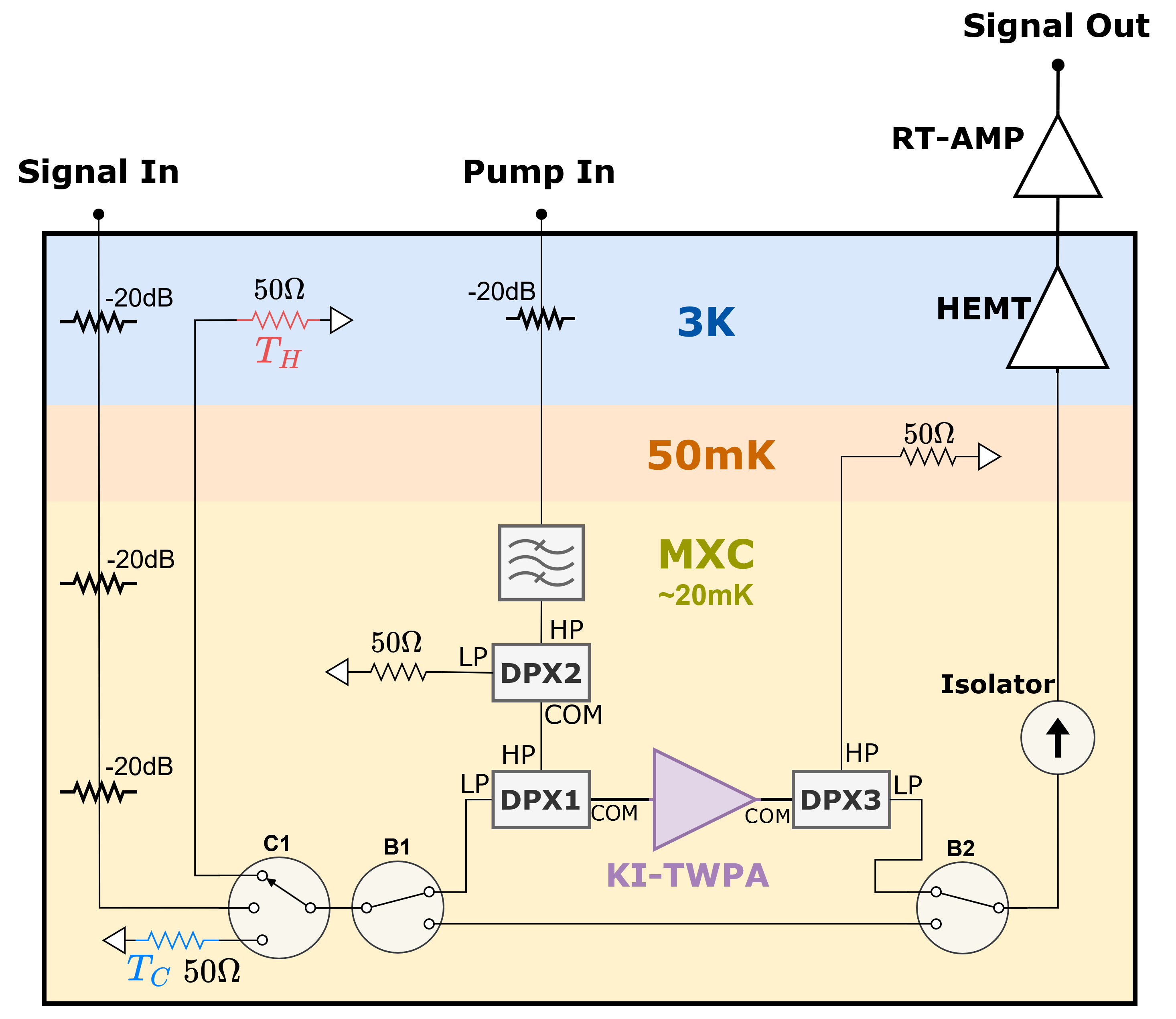
Appendix A Noise Measurement Setup
The input line is sufficiently attenuated from room temperature to the MXC stage using a combination of attenuators placed on the 3 K stage and MXC of the dilution refrigerator. For calibration and y-factor measurements, we utilized three relay switches at the MXC. Switch (Fig. 5) is used to switch between the input of the cryostat and the hot and cold terminations. Switches and are synced up and operated to switch between the KI-TWPA and a cryogenic cable for calibration. The amplified signal then passes through an isolator (on MXC) and a cryogenic HEMT amplifier at the 3 K stage, further amplified by a room temperature low noise amplifier, and finally read out using a spectrum analyzer.
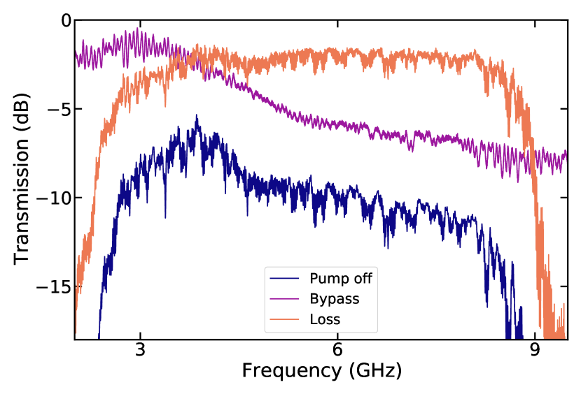
The pump input was filtered using a bandpass filter at the MXC stage and directed to the KI-TWPA using DPX 2 and 1 as illustrated in Fig 5a. Using the highpass port of DPX 3, the pump tone is terminated at the 50 mK stage of the dilution fridge. The total transmission of the system through the device was measured using a VNA with the pump tone off and the transmission of the cable bypassing the KI-TWPA and the diplexers as shown in Fig. 5.a. The plots comparing the transmission between the cryogenic cable and the unpumped KI-TWPA are shown in Fig. 5.b and labeled as ‘Bypass’ and ‘Pump off,’ respectively. The net loss from DPX 1 placed between the KI-TWPA and switch C1 in the circuit is also plotted in Fig. 5.b as ‘Loss.’
Appendix B Noise Theory
To model the noise in the setup, we used the circuit diagram shown in Fig. 4.b. If we assume the mK losses in the components between the noise sources (hot & cold in this case) and the KI-TWPA are and , the cascaded noise equations can be written as follows:
| (7) | ||||
| (8) | ||||
| (9) | ||||
| (10) | ||||
| (11) |
Where is the input noise of the 50 terminations. is the quantum noise and for is equal to one half. and are the gain and added noise of the KI-TWPA and the HEMT amplifier, respectively. is the additional effective warm amplification, and is the total noise measured on the spectrum analyzer (SA).
When the KI-TWPA is pumped, the total noise measured by the SA can be calculated using equations (B1-B5).
| (12) |
where , and are defined as follows.
| (13) |
| (14) |
| (15) |
By switching to a hot and a cold load, therefore varying the input noise, we can extract the system noise
| (16) |
When the KI-TWPA is unpumped, we can treat it as a lossless transmission line. Using the cascaded noise equations, we arrive at the following equation for the total noise measured at the SA with the pump off.
| (17) |
If we bypass the KI-TWPA and all the components between the noise source and the HEMT amplifier, the total noise measured at SA is
| (18) |
Then the added noise of the KI-TWPA is
| (19) |
In the above equations, the loss factors and can be estimated either by measuring insertion losses of the components separately or using the bypass and pump-off transmission measurements using the relay switches. can be estimated using either equation (B 12) or (B 11) with a y-factor measurement. Finally, measuring the gain of the KI-TWPA, we can calculate the added noise of the TWPA from the above equation. Using the unpumped KI-TWPA noise spectra, we measure an average HEMT noise temperature of 5 kelvin, which is in agreement with LNF-LNC0.3_14B datasheet.
Improve it In Fig. 5.b, you can see the transmission () measurements of the cable in two scenarios. The first one is the bypassing of KI-TWPA, represented by the orange line, and the second one is the transmission through DPX2, KI-TWPA, and DPX3, represented by the blue line. We have calculated the loss between switch B1 and the KI-TWPA by subtracting the unpumped measurement from the bypass measurement and dividing it by two since we used identical diplexers with similar insertion loss. This calculated loss is plotted as a green line in Fig. 5.b as a function of frequency, and we have used it as L1 and L2 loss factors in the main text.
References
- Zobrist et al. (2019) N. Zobrist et al., “Wide-band parametric amplifier readout and resolution of optical microwave kinetic inductance detectors,” Applied Physics Letters 115, 042601 (2019), https://pubs.aip.org/aip/apl/article-pdf/doi/10.1063/1.5098469/14525680/042601_1_online.pdf .
- Kempf et al. (2017) S. Kempf et al., “Demonstration of a scalable frequency-domain readout of metallic magnetic calorimeters by means of a microwave SQUID multiplexer,” AIP Advances 7, 015007 (2017), https://pubs.aip.org/aip/adv/article-pdf/doi/10.1063/1.4973872/12927237/015007_1_online.pdf .
- Malnou et al. (2023a) M. Malnou et al., “Improved microwave SQUID multiplexer readout using a kinetic-inductance traveling-wave parametric amplifier,” Applied Physics Letters 122, 214001 (2023a), https://pubs.aip.org/aip/apl/article-pdf/doi/10.1063/5.0149646/17832018/214001_1_5.0149646.pdf .
- Peng et al. (2022) K. Peng et al., “Floquet-mode traveling-wave parametric amplifiers,” PRX Quantum 3 (2022), 10.1103/prxquantum.3.020306.
- Barzanjeh, DiVincenzo, and Terhal (2014) S. Barzanjeh, D. P. DiVincenzo, and B. M. Terhal, “Dispersive qubit measurement by interferometry with parametric amplifiers,” Physical Review B 90 (2014), 10.1103/physrevb.90.134515.
- Didier et al. (2015) N. Didier, A. Kamal, W. D. Oliver, A. Blais, and A. A. Clerk, “Heisenberg-limited qubit read-out with two-mode squeezed light,” Physical Review Letters 115 (2015), 10.1103/physrevlett.115.093604.
- Ramanathan et al. (2023) K. Ramanathan et al., “Wideband direct detection constraints on hidden photon dark matter with the qualiphide experiment,” Phys. Rev. Lett. 130, 231001 (2023).
- Aumentado (2020) J. Aumentado, “Superconducting parametric amplifiers: The state of the art in josephson parametric amplifiers,” IEEE Microwave Magazine 21, 45–59 (2020).
- Esposito et al. (2021) M. Esposito et al., “Perspective on traveling wave microwave parametric amplifiers,” Applied Physics Letters 119 (2021), 10.1063/5.0064892.
- Mutus et al. (2013) J. Mutus et al., “Design and characterization of a lumped element single-ended superconducting microwave parametric amplifier with on-chip flux bias line,” Applied Physics Letters 103 (2013).
- Macklin et al. (2015) C. Macklin et al., “A near–quantum-limited josephson traveling-wave parametric amplifier,” Science 350, 307–310 (2015), https://www.science.org/doi/pdf/10.1126/science.aaa8525 .
- Shu et al. (2021) S. Shu, N. Klimovich, B. H. Eom, A. D. Beyer, R. B. Thakur, H. G. Leduc, and P. K. Day, “Nonlinearity and wide-band parametric amplification in a (nb,ti)n microstrip transmission line,” Physical Review Research 3 (2021), 10.1103/physrevresearch.3.023184.
- Malnou et al. (2021) M. Malnou et al., “Three-wave mixing kinetic inductance traveling-wave amplifier with near-quantum-limited noise performance,” PRX Quantum 2, 010302 (2021).
- Eom et al. (2012) B. Eom, P. K. Day, H. G. LeDuc, and J. Zmuidzinas, “A wideband, low-noise superconducting amplifier with high dynamic range,” Nature Physics 8, 623–627 (2012).
- Ranzani et al. (2018) L. Ranzani et al., “Kinetic inductance traveling-wave amplifiers for multiplexed qubit readout,” Applied Physics Letters 113, 242602 (2018), https://pubs.aip.org/aip/apl/article-pdf/doi/10.1063/1.5063252/14520906/242602_1_online.pdf .
- Vissers et al. (2016) M. R. Vissers et al., “Low-noise kinetic inductance traveling-wave amplifier using three-wave mixing,” Applied Physics Letters 108, 012601 (2016), https://pubs.aip.org/aip/apl/article-pdf/doi/10.1063/1.4937922/12854602/012601_1_online.pdf .
- Chaudhuri et al. (2017) S. Chaudhuri et al., “Broadband parametric amplifiers based on nonlinear kinetic inductance artificial transmission lines,” Applied Physics Letters 110, 152601 (2017), https://pubs.aip.org/aip/apl/article-pdf/doi/10.1063/1.4980102/14495669/152601_1_online.pdf .
- Shan, Sekimoto, and Noguchi (2016) W. Shan, Y. Sekimoto, and T. Noguchi, “Parametric amplification in a superconducting microstrip transmission line,” IEEE Transactions on Applied Superconductivity 26, 1–9 (2016).
- Boc (2014) “Development of a broadband nbtin traveling wave parametric amplifier for mkid readout,” (2014).
- Klimovich (2022) N. S. Klimovich, Traveling wave parametric amplifiers and other nonlinear kinetic inductance devices, Ph.D. thesis (2022).
- Kerr and Feldman (1996) A. Kerr and M. J. Feldman, “Mma memo 161 receiver noise temperature, the quantum noise limit, and the role of the zero-point fluctuations *,” (1996).
- Malnou et al. (2023b) M. Malnou et al., “Low-noise cryogenic microwave amplifier characterization with a calibrated noise source,” (2023b), arXiv:2312.14900 [quant-ph] .