Strain fingerprinting of exciton valley character
Abstract
Abstract: Momentum-indirect excitons composed of electrons and holes in different valleys define optoelectronic properties of many semiconductors, but are challenging to detect due to their weak coupling to light. The identification of an excitons’ valley character is further limited by complexities associated with momentum-selective probes. Here, we study the photoluminescence of indirect excitons in controllably strained prototypical 2D semiconductors (WSe2, WS2) at cryogenic temperatures. We find that these excitons i) exhibit valley-specific energy shifts, enabling their valley fingerprinting, and ii) hybridize with bright excitons, becoming directly accessible to optical spectroscopy methods. This approach allows us to identify multiple previously inaccessible excitons with wavefunctions residing in K, , or Q valleys in the momentum space as well as various types of defect-related excitons. Overall, our approach is well-suited to unravel and tune intervalley excitons in various semiconductors.
Introduction
Two-dimensional semiconductors from the family of transition metal dichalcogenides (TMDs) host a wide variety of excitons, Coulomb-bound electron-hole pairs. The electron/hole wavefunctions for the most relevant excitons reside at the extrema of conduction (CB) and valence bands (VB) at the K, K’, Q, and points of the Brillouin zone[1, 2]. Much of the early research was devoted to momentum-direct excitons with electron and hole wavefunctions in K valley (KK neutral excitons, charged excitons, biexcitons, etc.). These quasiparticles with large oscillator strength directly couple to light and exhibit prominent features in the optical absorption and emission spectra[1, 3, 4, 5]. However, these ”bright” species are only a small subset of excitons in TMDs. Recent studies show that the optoelectronic properties of TMDs are largely defined by a much more diverse class of ”dark” momentum-indirect intervalley excitons X, quasiparticles with hole and electron wavefunctions residing in the valleys A (= K, ) and B (= K’, Q), respectively[6, 7, 8]. Some of these quasiparticles, e.g., X, constitute the excitonic ground state of several TMDs, e.g., monolayers of WSe2, WS2, and bilayers[2, 9]. These states weakly interact with light, show several orders of magnitude longer lifetimes, and exhibit long diffusion lengths compared to their direct counterparts[6, 10]. Therefore, the long-range spatial transport and temporal dynamics observed in these materials are defined by the interactions and interconversion between direct and indirect excitons[6, 11]. The long lifetime of indirect excitons makes them a prime candidate for the realization of many-body correlated states in TMDs[12, 13]. Defect-related excitons constitute another class of quasiparticles with distinct momentum character. The hole wavefunction for a defect exciton resides in the K-valley of the VB, while the electron wavefunction (typically localized at a point defect) is represented by the momentum-delocalized defect states (D) near the CB[14, 15, 16]. These defect-related excitons critically contribute to the long spin/valley lifetime and carrier dynamics in TMDs[14].
Despite multiple studies suggesting the defining role of momentum-indirect excitons in the optical and transport properties of TMDs, they are much less studied compared to their direct counterparts. The key challenge is that the conventional optical spectroscopy approaches cannot directly differentiate between the excitons residing in different valleys as they are hampered by the lack of momentum resolution and the low oscillator strength of these quasiparticles[17]. Additionally, some indirect excitons such as X or X lie in energetic proximity of a series of tightly-bound KK excitons (trions, biexcitons, etc.) further complicating their study. In principle, techniques such as angle-resolved photoemission spectroscopy (ARPES) or electron energy loss spectroscopy (EELS) provide the momentum resolution needed to identify the momentum-indirect states[18, 19, 20, 21, 22]. However, the typical separation between the excitonic species (10 meV) in TMDs is much smaller compared to the energy resolution of these techniques. These approaches also require large-area devices and are challenging to integrate with external stimuli such as electric and magnetic fields.
In this work, we identify the valley character of momentum-indirect excitons in TMDs. We tackle the challenges outlined above by studying the response of excitonic photoluminescence (PL) peaks to mechanical strain at cryogenic temperatures. We show that the exciton’s energy changes with strain at a rate characteristic of the valleys in which its electron and hole wavefunctions reside, allowing straightforward identification of the exciton valley character — ”valley fingerprinting”. Moreover, a distinct strain response implies that at a specific strain value, the indirect excitons can be brought into energetic resonance with the momentum-direct bright excitons. The hybridization between these species brightens the dark states allowing their optical detection. We use our technique to directly observe and identify previously hypothesized, but experimentally inaccessible intervalley KQ and Q excitons. In addition, we fingerprint the fine structure of well-known KK excitons and several types of defect-related excitons. Finally, we achieve in-situ strain tuning of quantum-confined excitons associated with single photon emitters by up to meV. In a larger context, our work establishes strain engineering as a tool to identify the valley character of excitons, to tune them, and to explore inter-excitonic interactions.
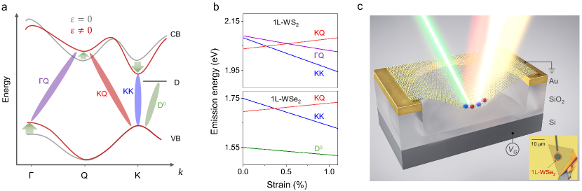
Results
Theoretical predictions for excitonic strain response. We start by analyzing the strain response of various intra- and inter-valley excitons in TMDs theoretically. First-principles calculations show[2, 23, 24, 25] that the CB minima () and the VB maxima () in different valleys (e.g., K, Q, ) as well as the defect state D react differently to an applied strain, (tensile biaxial strain unless stated otherwise). For example, the CB at the K valley shifts down in energy relative to the K valley VB with increasing tensile strain, the energy of the defect states remains nearly strain-independent, and the CB at the Q valley shifts up in energy (Fig. 1a). The behaviour of each valley is governed by the distinct strain dependence of the overlap of electronic orbitals constituting its wavefunctions, Fig. S1[23]. In general, the energy of an exciton X is given by , with the last term representing the exciton binding energy. Since the binding energy is only weakly strain-dependent, especially in K and Q valleys (Fig. S1), the strain response of an exciton is predominantly defined by its constituent valleys[25, 26]. The calculated strain response of various excitons in 1L-WSe2 and 1L-WS2 supports this intuition (Fig. 1b; see Notes S1 and S2 for calculation details). For example, K/K’-valley excitons in 1L-WSe2 are predicted to redshift with a strain gauge factor meV/%. The Q excitons also redshift in 1L-WS2, although at a lower rate meV/%. A Q exciton in 1L-WSe2 is expected to lie 270 meV above the KK exciton and therefore is not considered in our study, Fig. S1[2]. The KQ excitons in 1L-WSe2 shift in energy under tensile strain with meV/% while a localized defect-related exciton D is only weakly strain-dependent, meV/%.
The calculations in Fig. 1b reveal the following key traits. First, from the strain response of an exciton alone one can, in principle, determine its valley character. Second, because different intervalley excitons shift in energy with strain at different rates, we can control the energy separation and hence the coupling between them. This, in turn, enables novel interactions such as brightening of an otherwise dark X or D exciton via hybridization with a bright X exciton[6, 14, 27]. While these ideas have already been applied to examine the strain response and hybridization between intervalley excitons,[6, 28, 29, 30, 31, 32, 33, 34] most strain-engineering techniques function only at room temperature. Under these conditions, temperature-related exciton linewidth broadening and thermal dissociation severely limit the range of accessible excitonic species. Examining the full range of intervalley excitons and studying their interactions therefore requires low-disorder TMD devices with in-situ strain control up to a few percent at cryogenic temperature.
Experimental realization of exciton valley fingerprinting. To address these requirements, we use the electrostatic straining technique we recently developed[27] (Fig. 1c). A monolayer flake is suspended over a circular trench in a Au/SiO2/Si substrate where an applied gate voltage () induces biaxial strain in the center of the membrane via electrostatic forces. The device is placed inside a cryostat ( K), while its PL response to an optical excitation is measured as a function of strain in the center of the suspended flake (see Methods). The induced strain is symmetric with respect to the polarity (Fig. S2) and reaches , limited by the dielectric breakdown of SiO2.
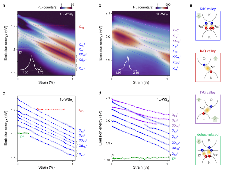
Figure 2a and 2b show photoluminescence emission spectra vs. strain of 1L-WSe2 and 1L-WS2, respectively (see Note S4, Fig. S3 for strain determination). Both material systems exhibit complex spectra with an abundance of excitonic peaks (insets of Fig. 2a,b). Some well-known excitons such as neutral and charged excitons (X, X), charged biexcitons (XX), dark trions (Xd) and their phonon replicas can be identified at zero strain by comparing their peak positions and power dependence with previous reports[35, 36, 37] (Fig. S4, S5). Once the strain is applied, different groups of peaks exhibit distinct strain dependence. We extract the energy positions of various excitonic peaks vs. strain and color-code each group of peaks based on their strain dependence (Fig. 2c,d). We now proceed to assign these peaks to the excitons residing in specific valleys of the electronic band structure.
KK valley excitons. We first focus on the largest group of peaks (X, X, XX, Xd ) shifting down in energy with gauge factor meV/% in 1L-WSe2 and meV/% in 1L-WS2 (blue in Fig. 2c,d). This is the shift expected for an optical transition between the VB and CB at the K/K’ valley (blue in Fig. 1b), in agreement with previous reports[39, 29, 31, 32, 33]. We find very close gauge factors for species within the KK group (Fig. S4). This similarity suggests that i) effects related to the carrier density changes with , estimated to be cm-2 in our technique[40], are insignificant compared to the strain-related effects (Fig. S4); ii) strain-related changes in the phonon energies are minor, since the energy spacing between excitons and their replicas depends on the phonon energy[26, 41]; and iii) effective masses near the K valley are nearly strain-independent (as suggested by theory, see Fig. S1) since the binding energy of the biexciton (determined from the energy difference between X and XX) is affected by strain only via the effective mass.
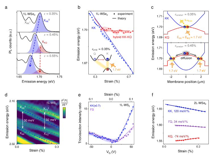
KQ excitons. We now turn to the nearly strain-independent peak at 1.70 eV in 1L-WSe2 (red in Fig. 2c). To assign the nature of this feature, we plot PL spectra at three applied strain values of 0.35%, 0.45%, and 0.55% (Fig. 3a). While X (blue shaded) and X redshift with strain, a new feature (red shaded) appears on the high-energy side of X above a critical strain value, %. This peak exhibits a linear power dependence suggesting its free excitonic character (Fig. S5) and emerges exactly at the strain value at which the X and X excitons are predicted to come into resonance ( in Fig. 1b; eV). We therefore suggest that the 1.70 eV peak corresponds to a hybridized state of KQ and KK excitons. In this scenario, a normally dark KQ exciton acquires oscillator strength through resonant hybridization with a bright KK exciton with which it shares the hole wavefunction (inset, Fig. 3b). The emerging hybrid state should emit only in the vicinity of while having a vanishing oscillator strength otherwise.
Notably, we observe that the peak at 1.70 eV persists for the applied strain exceeding 0.35% and its energy remains nearly strain-independent afterward (Fig. 3b). We ascribe this behavior to a slight parabolic strain variation () in our membrane around the maximum reached in the center (Fig. 3c, Fig. S6). With increasing , the strain first reaches the critical value in the center of the membrane (Fig. 3c, top panel). When the applied strain exceeds 0.35%, the condition required for the KK-KQ hybridization progressively shifts outward from the center of the membrane in a donut-shaped region (Fig. 3c, bottom panel). Therefore, the emission at 1.70 eV persists even for and remains strain independent (Fig. 3a,b). Our theoretical many-particle model for the KK-KQ hybridization accounting for a strain inhomogeneity ( approximated by a gaussian distribution of FWHM 6.1 m) and X diffusion[6] confirms the strain-independent behaviour (solid lines in Fig. 3b; see Note S3 for details). Decrease of the hybrid exciton intensity for further supports our model (Fig. S7). We also observe signatures of a similar peak in 1L-WS2 in the predicted hybridization regime (Fig. S8). The apparent brightness of hybrid excitons at large strain values () may be further influenced by high strain non-uniformity near the membrane edges—this effect could be reduced by increasing the membrane diameter. We note that the KQ excitons were previously reported in ARPES measurements[18] and invoked to explain excitonic transport[6, 42] but, to the best of our knowledge, have never been directly seen before via optical spectroscopy techniques.
While the strain response of the KQ exciton in a monolayer is governed by hybridization, its fingerprinting is more straightforward in a bilayer WSe2 (Fig. 3f). Here, the KQ emission is more intense due to an abundance of phonons mitigating excess momentum and a significantly lower energy of X compared to X ensuring its higher population[9]. Indeed, we observe a low-intensity peak 120 meV below X shifting up in energy as predicted for a KQ exciton[43] (Fig. S1, S9).
Q excitons. According to our calculations, the Q and the KK excitons in unstrained WS2 are nearly resonant, however, can be distinguished under strain due to distinct gauge factors. To this end, we note the group of three peaks in Fig. 2d (purple points) red shifting with gauge factor meV/%. This gauge factor as well as the energy of the states match theoretical expectations for Q excitons (Fig. 1b). Within this group, we assign the two highest lying states as neutral (X) and charged Q excitons (X), respectively. To support our assignment, we first note that the two states are separated by 32 meV, a value similar to the X binding energy of 30 meV[44] (Fig. 3d). Second, these states exhibit the characteristic behavior of the charged states, i.e., an increase of neutral to charged exciton conversion with increasing carrier density (Fig. 3e). Finally, we suggest that the lowest-energy Q state (52 meV below X in Fig. 2d) is of biexcitonic nature since it shows a super-linear dependence of PL on the excitation power (PL , Fig. S5). Further work is needed to pinpoint the exact configuration and brightening mechanism of this state[45]. We highlight that our suspended devices are ideally suited to study Q excitons: the X energy in a supported device is affected by screening[46] and is predicted to lie 50 meV higher with significantly weaker emission, rendering their observation challenging (Note S1). To the best of our knowledge, this is the first experimental observation of Q excitons in monolayers.
Another system where Q excitons have been theoretically predicted is bilayer WSe2 (Fig. 3f). There, the and the K valleys are nearly degenerate in the VB and a Q exciton is predicted to lie 50 meV above their KK counterpart, Fig. S1). Indeed, our PL data for bilayer WSe2 indicate a state 70 meV below X shifting down in energy with a rate of meV/%, consistent with the expected gauge factors for Q excitons in this material[9] (Fig. S1, S9). We note that, unlike in the monolayer case, additional effects such as heterostrain or change in layer separation may complicate the strain response of bilayers.
Localized excitons. Having identified most of the free excitons, we now proceed to the emission features of localized states distinguished by sublinear power dependence (Fig. S5). The energy of the peak labeled D in Fig. 2c (green) is nearly strain-independent ( meV/%), suggesting that the valleys hosting the corresponding electron/hole wavefunctions shift with strain at nearly equivalent rates. Comparison with Fig. 1b allows us to identify D as a chalcogen-vacancy-related defect exciton, consistent with previous study[27]. This state involves an optical transition between the VB at the K-point and the momentum-delocalized defect state below the CB (Fig. 1b). Interestingly, also the peaks 120 meV and 150 meV below X, labelled X, exhibit sublinear power dependence. These peaks, however, exhibit a gauge factor meV/%, close to that of KK excitons. We therefore attribute the peaks, X, to the recombination of a neutral KK exciton bound to a defect. Indeed, states in the same energy range have been recently ascribed to defect-bound excitons[35].
A similar scenario is observed in 1L-WS2 (Fig. 2d): the strain-independent peak D appears near 1.75 eV, and the X peak 1.97 eV (at ). The energy difference between D and X is larger in WS2 compared to WSe2 (340 vs. 150 meV), suggesting different defect energy levels involved in the corresponding optical transitions (Fig. S1). We see that, in principle, the strain response allows distinguishing between various types of defect-related excitons including two-particle (e.g., D) or three-particle (X) states.
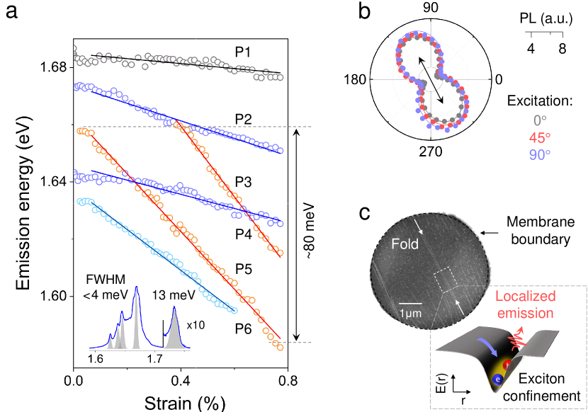
In addition to D and X consistently seen in multiple devices, in some devices we observe additional localized exciton peaks. Figure 4 shows strain response in one such WSe2 sample where we identify a group of closely lying peaks labeled P1—P6 with various gauge factors in the range meV/%. These peaks are 4 times narrower than X (inset in Fig. 4a), have a preferred emission direction independent of the excitation (Fig. 4b, Fig. S10), and show sublinear power dependence (Fig. S10). These features are tell-tale signs of extensively studied[47, 48, 49, 50] single-photon emitters in WSe2. A locally inhomogeneous strain profile has been suggested as the critical requirement for the formation of such emitters via exciton confinement[14, 27]. Indeed, the scanning electron microscope (SEM) image of this device shows the presence of folds across the membrane (Fig. 4c, Fig. S10) that could lead to sharp (up to 0.02 %/nm) strain gradients[51, 52]. Notably, the PL polarization from peaks P1—P6 is oriented along those folds confirming exciton confinement (Fig. 4b). The variation in the gauge factors is then likely associated with the effect of the externally applied strain on the inhomogeneous strain present in the fold. Crucially, the energy of emitters P1—P6 can be tuned by up to 80 meV under the application of strain. That is the largest reported tuning for such states, to the best of our knowledge[53, 54]. Moreover, two distinct states can be brought into an energetic resonance at specific strain values resulting in enhanced emission (Fig. S10), possibly caused by exciton population redistribution[55]. These observations suggest the potential of confined states with engineered strain gauge factors to control exciton hybridization. In the future, measurements are of particular interest for proving the indistinguishability of such resonant states[56].
Discussion
To summarize, we established mechanical strain as a powerful tool to brighten the momentum-indirect dark excitons and fingerprint their valley character. In our approach, in-situ control over mechanical strain at low temperatures is the key to unveiling the complex excitonic landscape of 1L-WSe2, 1L-WS2, and 2L-WSe2. We established the valley character of previously inaccessible Q excitons/trions, KQ excitons in addition to the defect-related excitons (Table 1). We also identified a brightening mechanism for the normally dark KQ excitons via strain-driven hybridization with bright excitons. Finally, we showed wide-range strain tuning of the energy of quantum-confined excitons in 1L-WSe2 opening pathway to broadly tunable quantum emitters. We note that our current samples have broader excitonic linewidth compared to the hBN-encapsulated devices[35, 40]. Superior samples with narrower linewidth will enhance the control over closely lying excitonic species. Devices with
| WSe2 | WS2 | ||||||||||||||||||
|---|---|---|---|---|---|---|---|---|---|---|---|---|---|---|---|---|---|---|---|
| KK | KQ | Defect | KK | Q | Defect | ||||||||||||||
| X | X | XX | X | X | D | X | X | XX | X | X | X | XX | D | ||||||
| , eV | 1.74 | 1.72 | 1.70 | 1.64 | 1.69* | 1.60 | 2.08 | 2.05 | 2.03 | 1.98 | 2.09 | 2.06 | 2.04 | 1.76 | |||||
| , meV/% | 118 | 114 | 113 | 103 | -34* | 8 | 102 | 101 | 100 | 100 | 68 | 55 | 56 | -6 | |||||
| 0.97 | 1.11 | 1.42 | 0.70 | 0.95 | 0.66 | 0.97 | 0.99 | 1.33 | 0.86 | 1.01 | 1.18 | 1.36 | 0.50 | ||||||
engineered strain inhomogeneity may allow us to better manipulate the quantum emitters, spatially modulate exciton hybridization, and guide exciton transport. Extension of the simulations to account for non-linear effects and inhomogeneous strain might be required beyond the linear strain regime analyzed here.
Our approach to brighten and fingerprint intervalley excitons via strain engineering opens multiple possibilities for future research. First, it may be applied to identify the valley character of excitons in other systems such as moiré TMD heterostructures[57], perovskites[58, 59], and 2D magnets[60, 61]. Second, our technique enables optical control of spins in the Q valley that remained unexplored until now[62]. The spin/valley locked KQ excitons should exhibit a long lifetime and diffusion length, hence may prove advantageous for spin-/valleytronics compared to the direct excitons[6, 10, 63]. We expect a pronounced strain-dependence of the transport dynamics and the lifetimes of these excitons. Third, our approach may be capable of detecting strain-dependent changes in the effective masses of excitons[26], controlling exciton-phonon interactions (by modulating the energy separation between the states involved)[28, 40, 45], and distinguishing different types of defects (since various defect states exhibit distinct strain response)[14, 27]. The application of uniaxial strain may further break the symmetry of our system thereby changing the band topology of the corresponding excitons[64]. This enables unique prospects to manipulate valley pseudospins via large in-plane pseudo magnetic fields[65, 66].
Methods
Sample fabrication The devices were fabricated by dry transfer of mechanically exfoliated TMD flakes onto a circular trench (diameter is 5 m) wet etched via Hydrofluoric (HF) acid in Au/Cr/SiO2/Si stack. The strain in the membrane is induced by applying a gate voltage (typically in the range of up to 210 V) between the TMD flake (electrically grounded) and the Si back gate of the chip. The strain in the center was characterized using laser interferometry (see Note S4).
Optical measurements The devices were measured inside a cryostat (CryoVac Konti Micro) at a base temperature of 10 K. The PL measurements were carried out using the Spectrometer Kymera 193i Spectrograph, while CW lasers with nm (10 W) and nm (6 W) tightly focused in the center of the membrane with spot diameter 1 m were used to excite WS2 and WSe2, respectively. Polarization-resolved PL measurements were performed using a combination of a half-wave plate (RAC 4.2.10, B. Halle) and an analyzer (GL 10, Thorlabs) before the spectrometer to select specific polarization. The fold was confirmed using a Scanning Electron Microscopy (SEM) system Raith Pioneer II SEM/EBL at an accelerating voltage of kV.
Acknowledgements
The Berlin group acknowledges the Deutsche Forschungsgemeinschaft (DFG) for financial support through the Collaborative Research Center TRR 227 Ultrafast Spin Dynamics (project B08 and the Federal Ministry of Education and Research (BMBF, Projekt 05K22KE3). The Marburg group acknowledges financial support by the DFG via SFB 1083 (project B9) and the regular project 512604469. The Vienna group acknowledges financial support by The Austrian Science Fund (FWF) through doctoral college TU-DX (DOC 142-N) and the DOC-fellowship of the Austrian Academy of Sciences. P.H.L. and S.H. acknowledge funding from the DFG under the Emmy Noether Initiative (project-ID 433878606).
Author Contributions
A.K., D.Y., and K.I.B. conceived the project. A.K., D.Y., and C.G. designed the experimental setup. A.K., D.Y., D.J.B., B.H., and K.B. prepared the samples. S.H. and P.H.L. developed the electrostatic straining technique. A.K., D.Y., and D.J.B. performed the optical measurements. R.R., J.H., and E.M. developed theory for excitons. C.S., S.T., and F.L. developed the theory for defect states. J.N.K. performed mechanical simulations. A.K. and D.Y. analyzed the data. A.K., D.Y., and K.I.B. wrote the manuscript with input from all co-authors.
Data Availability Statement
The data that support the findings of this study are available from the corresponding author upon reasonable request.
The authors declare no competing financial interest.
References
- Wang et al. [2018] G. Wang, A. Chernikov, M. M. Glazov, T. F. Heinz, X. Marie, T. Amand, and B. Urbaszek, Reviews of Modern Physics 90, 021001 (2018).
- Malic et al. [2018] E. Malic, M. Selig, M. Feierabend, S. Brem, D. Christiansen, F. Wendler, A. Knorr, and G. Berghäuser, Physical Review Materials 2, 014002 (2018).
- He et al. [2014] K. He, N. Kumar, L. Zhao, Z. Wang, K. F. Mak, H. Zhao, and J. Shan, Physical review letters 113, 026803 (2014).
- Chernikov et al. [2014] A. Chernikov, T. C. Berkelbach, H. M. Hill, A. Rigosi, Y. Li, B. Aslan, D. R. Reichman, M. S. Hybertsen, and T. F. Heinz, Physical review letters 113, 076802 (2014).
- Mak et al. [2013] K. F. Mak, K. He, C. Lee, G. H. Lee, J. Hone, T. F. Heinz, and J. Shan, Nature Materials 12, 207 (2013).
- Rosati et al. [2021] R. Rosati, R. Schmidt, S. Brem, R. Perea-Causín, I. Niehues, J. Kern, J. A. Preuß, R. Schneider, S. Michaelis de Vasconcellos, R. Bratschitsch, and E. Malic, Nature Communications 12 (2021), 10.1038/s41467-021-27425-y.
- [7] M. Selig, G. Berghäuser, A. Raja, P. Nagler, C. Schüller, T. F. Heinz, T. Korn, A. Chernikov, E. Malic, and A. Knorr, Nature Communications 7, 10.1038/ncomms13279.
- Selig et al. [2018] M. Selig, G. Berghäuser, M. Richter, R. Bratschitsch, A. Knorr, and E. Malic, 2D Materials 5, 035017 (2018).
- Lindlau et al. [2018] J. Lindlau, M. Selig, A. Neumann, L. Colombier, J. Förste, V. Funk, M. Förg, J. Kim, G. Berghäuser, T. Taniguchi, K. Watanabe, F. Wang, E. Malic, and A. Högele, Nature Communications 9, 2586 (2018).
- Zipfel et al. [2020] J. Zipfel, M. Kulig, R. Perea-Causín, S. Brem, J. D. Ziegler, R. Rosati, T. Taniguchi, K. Watanabe, M. M. Glazov, E. Malic, et al., Physical Review B 101, 115430 (2020).
- Chand et al. [2023] S. B. Chand, J. M. Woods, J. Quan, E. Mejia, T. Taniguchi, K. Watanabe, A. Alù, and G. Grosso, Nature Communications 14, 3712 (2023).
- Rivera et al. [2018] P. Rivera, H. Yu, K. L. Seyler, N. P. Wilson, W. Yao, and X. Xu, Nature Nanotechnology 13, 1004 (2018).
- Yagodkin et al. [2023] D. Yagodkin, A. Kumar, E. Ankerhold, J. Richter, K. Watanabe, T. Taniguchi, C. Gahl, and K. I. Bolotin, Nano Letters 23 (2023), 10.1021/acs.nanolett.3c01708.
- Linhart et al. [2019] L. Linhart, M. Paur, V. Smejkal, J. Burgdörfer, T. Mueller, and F. Libisch, Physical Review Letters 123 (2019), 10.1103/PhysRevLett.123.146401.
- Yagodkin et al. [2022] D. Yagodkin, K. Greben, A. Eljarrat, S. Kovalchuk, M. Ghorbani‐Asl, M. Jain, S. Kretschmer, N. Severin, J. P. Rabe, A. V. Krasheninnikov, C. T. Koch, and K. I. Bolotin, Advanced Functional Materials 32 (2022), 10.1002/adfm.202203060.
- Greben et al. [2020] K. Greben, S. Arora, M. G. Harats, and K. I. Bolotin, Nano Letters 20, 2544 (2020).
- Deilmann and Thygesen [2019] T. Deilmann and K. S. Thygesen, 2D Materials 6, 035003 (2019).
- Madéo et al. [2020] J. Madéo, M. K. Man, C. Sahoo, M. Campbell, V. Pareek, E. L. Wong, A. Al-Mahboob, N. S. Chan, A. Karmakar, B. M. K. Mariserla, X. Li, T. F. Heinz, T. Cao, and K. M. Dani, Science 370 (2020), 10.1126/science.aba1029.
- Dong et al. [2021] S. Dong, M. Puppin, T. Pincelli, S. Beaulieu, D. Christiansen, H. Hübener, C. W. Nicholson, R. P. Xian, M. Dendzik, Y. Deng, Y. W. Windsor, M. Selig, E. Malic, A. Rubio, A. Knorr, M. Wolf, L. Rettig, and R. Ernstorfer, Natural Sciences 1, e10010 (2021).
- Hong et al. [2020] J. Hong, R. Senga, T. Pichler, and K. Suenaga, Physical Review Letters 124 (2020), 10.1103/PhysRevLett.124.087401.
- Schmitt et al. [2022] D. Schmitt, J. P. Bange, W. Bennecke, A. AlMutairi, G. Meneghini, K. Watanabe, T. Taniguchi, D. Steil, D. R. Luke, R. T. Weitz, S. Steil, G. S. M. Jansen, S. Brem, E. Malic, S. Hofmann, M. Reutzel, and S. Mathias, Nature 608 (2022), 10.1038/s41586-022-04977-7.
- Wallauer et al. [2021] R. Wallauer, R. Perea-Causin, L. Münster, S. Zajusch, S. Brem, J. Güdde, K. Tanimura, K.-Q. Lin, R. Huber, E. Malic, and U. Höfer, Nano Letters 21, 5867 (2021).
- Feierabend et al. [2017] M. Feierabend, A. Morlet, G. Berghäuser, and E. Malic, Physical Review B 96 (2017), 10.1103/PhysRevB.96.045425.
- Zollner et al. [2019] K. Zollner, P. E. F. Junior, and J. Fabian, Physical Review B 100 (2019), 10.1103/PhysRevB.100.195126.
- Defo et al. [2016] R. K. Defo, S. Fang, S. N. Shirodkar, G. A. Tritsaris, A. Dimoulas, and E. Kaxiras, Physical Review B 94 (2016), 10.1103/PhysRevB.94.155310.
- Khatibi et al. [2019] Z. Khatibi, M. Feierabend, M. Selig, S. Brem, C. Linderälv, P. Erhart, and E. Malic, 2D Materials 6 (2019), 10.1088/2053-1583/aae953.
- Hernández López et al. [2022] P. Hernández López, S. Heeg, C. Schattauer, S. Kovalchuk, A. Kumar, D. J. Bock, J. N. Kirchhof, B. Höfer, K. Greben, D. Yagodkin, L. Linhart, F. Libisch, and K. I. Bolotin, Nature Communications 13, 7691 (2022).
- Niehues et al. [2018] I. Niehues, R. Schmidt, M. Drüppel, P. Marauhn, D. Christiansen, M. Selig, G. Berghäuser, D. Wigger, R. Schneider, L. Braasch, R. Koch, A. Castellanos-Gomez, T. Kuhn, A. Knorr, E. Malic, M. Rohlfing, S. Michaelis de Vasconcellos, and R. Bratschitsch, Nano Letters 18 (2018), 10.1021/acs.nanolett.7b04868.
- Aslan et al. [2021] B. Aslan, C. Yule, Y. Yu, Y. J. Lee, T. F. Heinz, L. Cao, and M. L. Brongersma, 2D Materials 9 (2021), 10.1088/2053-1583/ac2d15.
- Harats et al. [2020] M. G. Harats, J. N. Kirchhof, M. Qiao, K. Greben, and K. I. Bolotin, Nature Photonics 14, 324 (2020).
- Schmidt et al. [2016] R. Schmidt, I. Niehues, R. Schneider, M. Drüppel, T. Deilmann, M. Rohlfing, S. M. d. Vasconcellos, A. Castellanos-Gomez, and R. Bratschitsch, 2D Materials 3 (2016), 10.1088/2053-1583/3/2/021011.
- Blundo et al. [2022] E. Blundo, P. E. F. Junior, A. Surrente, G. Pettinari, M. A. Prosnikov, K. Olkowska-Pucko, K. Zollner, T. Woźniak, A. Chaves, T. Kazimierczuk, et al., Physical Review Letters 129, 067402 (2022).
- Blundo et al. [2020] E. Blundo, M. Felici, T. Yildirim, G. Pettinari, D. Tedeschi, A. Miriametro, B. Liu, W. Ma, Y. Lu, and A. Polimeni, Physical Review Research 2, 012024 (2020).
- Kovalchuk et al. [2020] S. Kovalchuk, M. G. Harats, G. López-Polín, J. N. Kirchhof, K. Höflich, and K. I. Bolotin, 2D Materials 7 (2020), 10.1088/2053-1583/ab8caa.
- Rivera et al. [2021] P. Rivera, M. He, B. Kim, S. Liu, C. Rubio-Verdú, H. Moon, L. Mennel, D. A. Rhodes, H. Yu, T. Taniguchi, K. Watanabe, J. Yan, D. G. Mandrus, H. Dery, A. Pasupathy, D. Englund, J. Hone, W. Yao, and X. Xu, Nature Communications 12 (2021), 10.1038/s41467-021-21158-8.
- Rosati et al. [2020a] R. Rosati, K. Wagner, S. Brem, R. Perea-Causin, E. Wietek, J. Zipfel, J. D. Ziegler, M. Selig, T. Taniguchi, K. Watanabe, et al., ACS Photonics 7, 2756 (2020a).
- Rosati et al. [2020b] R. Rosati, S. Brem, R. Perea-Causín, R. Schmidt, I. Niehues, S. M. de Vasconcellos, R. Bratschitsch, and E. Malic, 2D Materials 8, 015030 (2020b).
- Kirchhof et al. [2022] J. N. Kirchhof, Y. Yu, G. Antheaume, G. Gordeev, D. Yagodkin, P. Elliott, D. B. De Araújo, S. Sharma, S. Reich, and K. I. Bolotin, Nano letters 22, 8037 (2022).
- Carrascoso et al. [2021] F. Carrascoso, H. Li, R. Frisenda, and A. Castellanos-Gomez, Nano Research 14, 1698 (2021).
- Wagner et al. [2020] K. Wagner, E. Wietek, J. D. Ziegler, M. A. Semina, T. Taniguchi, K. Watanabe, J. Zipfel, M. M. Glazov, and A. Chernikov, Physical review letters 125, 267401 (2020).
- He et al. [2020] M. He, P. Rivera, D. Van Tuan, N. P. Wilson, M. Yang, T. Taniguchi, K. Watanabe, J. Yan, D. G. Mandrus, H. Yu, et al., Nature communications 11, 618 (2020).
- Berghäuser et al. [2018] G. Berghäuser, P. Steinleitner, P. Merkl, R. Huber, A. Knorr, and E. Malic, Physical Review B 98, 020301 (2018).
- Huang et al. [2022] Z. Huang, Y. Zhao, T. Bo, Y. Chu, J. Tian, L. Liu, Y. Yuan, F. Wu, J. Zhao, L. Xian, K. Watanabe, T. Taniguchi, R. Yang, D. Shi, L. Du, Z. Sun, S. Meng, W. Yang, and G. Zhang, Physical Review B 105 (2022), 10.1103/PhysRevB.105.L041409.
- Perea-Causin et al. [2023] R. Perea-Causin, S. Brem, O. Schmidt, and E. Malic, “Trion photoluminescence and trion stability in atomically thin semiconductors,” (2023).
- Brem et al. [2020] S. Brem, A. Ekman, D. Christiansen, F. Katsch, M. Selig, C. Robert, X. Marie, B. Urbaszek, A. Knorr, and E. Malic, Nano Letters 20 (2020), 10.1021/acs.nanolett.0c00633.
- Klots et al. [2018] A. R. Klots, B. Weintrub, D. Prasai, D. Kidd, K. Varga, K. A. Velizhanin, and K. I. Bolotin, Scientific reports 8, 768 (2018).
- Chakraborty et al. [2015] C. Chakraborty, L. Kinnischtzke, K. M. Goodfellow, R. Beams, and A. N. Vamivakas, 10, 507 (2015).
- 43 [2015] 10, 497 (2015).
- Srivastava et al. [2015] A. Srivastava, M. Sidler, A. V. Allain, D. S. Lembke, A. Kis, and A. Imamoglu, Nature Nanotechnology 10 (2015), 10.1038/nnano.2015.60.
- Koperski et al. [2015] M. Koperski, K. Nogajewski, A. Arora, V. Cherkez, P. Mallet, J.-Y. Veuillen, J. Marcus, P. Kossacki, and M. Potemski, Nature Nanotechnology 10 (2015), 10.1038/nnano.2015.67.
- Khan et al. [2020] A. R. Khan, T. Lu, W. Ma, Y. Lu, and Y. Liu, Advanced Electronic Materials 6, 1901381 (2020).
- Castellanos-Gomez et al. [2013] A. Castellanos-Gomez, R. Roldán, E. Cappelluti, M. Buscema, F. Guinea, H. S. Van Der Zant, and G. A. Steele, Nano Letters 13, 5361 (2013).
- Toth and Aharonovich [2019] M. Toth and I. Aharonovich, Annual Review of Physical Chemistry 70, 123 (2019).
- Iff et al. [2019] O. Iff, D. Tedeschi, J. Martín-Sánchez, M. Moczała-Dusanowska, S. Tongay, K. Yumigeta, J. Taboada-Gutiérrez, M. Savaresi, A. Rastelli, P. Alonso-González, S. Höfling, R. Trotta, and C. Schneider, Nano Letters 19 (2019), 10.1021/acs.nanolett.9b02221.
- Savaresi et al. [2023] M. Savaresi, A. Martínez-Suárez, D. Tedeschi, G. Ronco, A. Hierro-Rodríguez, S. McVitie, S. Stroj, J. Aberl, M. Brehm, V. M. García-Suárez, M. B. Rota, P. Alonso-González, J. Martín-Sánchez, and R. Trotta, “Strain-induced dynamic control over the population of quantum emitters in two-dimensional materials,” (2023).
- Patel et al. [2010] R. B. Patel, A. J. Bennett, I. Farrer, C. A. Nicoll, D. A. Ritchie, and A. J. Shields, Nature photonics 4, 632 (2010).
- Barré et al. [2022] E. Barré, O. Karni, E. Liu, A. L. O’Beirne, X. Chen, H. B. Ribeiro, L. Yu, B. Kim, K. Watanabe, T. Taniguchi, et al., Science 376, 406 (2022).
- Dey et al. [2020] A. Dey, A. F. Richter, T. Debnath, H. Huang, L. Polavarapu, and J. Feldmann, ACS nano 14, 5855 (2020).
- Zhang et al. [2017] Y. Zhang, J. Yin, M. R. Parida, G. H. Ahmed, J. Pan, O. M. Bakr, J.-L. Brédas, and O. F. Mohammed, The Journal of Physical Chemistry Letters 8 (2017), 10.1021/acs.jpclett.7b01381.
- Cenker et al. [2022] J. Cenker, S. Sivakumar, K. Xie, A. Miller, P. Thijssen, Z. Liu, A. Dismukes, J. Fonseca, E. Anderson, X. Zhu, X. Roy, D. Xiao, J.-H. Chu, T. Cao, and X. Xu, Nature Nanotechnology 17, 256–261 (2022).
- Diederich et al. [2022] G. M. Diederich, J. Cenker, Y. Ren, J. Fonseca, D. G. Chica, Y. J. Bae, X. Zhu, X. Roy, T. Cao, D. Xiao, and X. Xu, Nature Nanotechnology 18, 23–28 (2022).
- Beaulieu et al. [2023] S. Beaulieu, S. Dong, V. Christiansson, P. Werner, T. Pincelli, J. D. Ziegler, T. Taniguchi, K. Watanabe, A. Chernikov, M. Wolf, L. Rettig, R. Ernstorfer, and M. Schüler, “Berry Curvature Signatures in Chiroptical Excitonic Transitions,” (2023).
- Kumar et al. [2021] A. Kumar, D. Yagodkin, N. Stetzuhn, S. Kovalchuk, A. Melnikov, P. Elliott, S. Sharma, C. Gahl, and K. I. Bolotin, Nano Letters 21, 7123 (2021).
- Yu et al. [2014] H. Yu, G. B. Liu, P. Gong, X. Xu, and W. Yao, Nature Communications 5 (2014), 10.1038/ncomms4876.
- Glazov et al. [2022] M. M. Glazov, F. Dirnberger, V. M. Menon, T. Taniguchi, K. Watanabe, D. Bougeard, J. D. Ziegler, and A. Chernikov, Physical Review B 106 (2022), 10.1103/PhysRevB.106.125303.
- Iakovlev and Glazov [2023] Z. Iakovlev and M. M. Glazov, 2D Materials (2023).