First-principles study of band gap tuning in Ge1-xPbxSe
Abstract
Narrow band gap and its tuning are important aspects of materials for their technological applications. In this context group IV-VI semiconductors are one of the interesting candidates. In this paper, we explore the possibility of band gap tuning in one of the family member of this family GeSe by using isoelectronic Pb doping. Our study is first principles based electronic structure calculations of Ge1-xPbxSe. This study reveals that the Ge-p and Se-p states are strongly hybridized in GeSe and shows a gap in the DOS at Ef in GeSe. This gap reduces systematically with simultaneous enhancement of the states in the near Ef region as a function of Pb doping. This leads tuning of the indirect band gap in GeSe via Pb doping. The results of the indirect band gap decrement are consistent with the experimental findings. We propose a mechanism where the electrostatic effect of dopant Pb cation could be responsible for these changes in the electronic structure of GeSe.
keywords:
, GeSe semiconductor , Band Gap Tuning , Electronic structure calculation1 Introduction
Group IV-VI semiconductors are one of the interesting materials from the past mainly due to their small energy band gap. Recent studies have revealed that these narrow energy gap materials serve an excellent ground for photoabsorption in near infrared and infrared regions of solar spectrum in their nano crystalline(NC) form which is quite useful to fabricate absorption layer of the photovoltaics[1, 2, 3]. Some of the anion alloyed NCs, like PbSxSe1-x and PbSxTe1-x have already been synthesized for tuning the energy gap[4, 5] in these regions of solar spectrum. These materials also show wide variation in the electrical and optical properties which make them useful in numerous applications, for example photovoltaic applications[8], long wavelength sensor devices[7] and infrared lasers[9, 10]. Furthermore, SnSe, GeSe, GeS, and SnS compounds of this group IV-VI family have been recognised as highly efficient materials for thermoelectricity because of their large Seeback coefficients, high power factor and low thermal conductivities[11]. Intermediate compounds of this family have also been formed for further investigating the properties of these materials. For example, currently Gharsallah et al. have claimed that Ge doping can enhance the thermoelectric efficiency of SnSe. They argue increase in the band gap could be the reason for record high Seeback coefficient observed in the lighter doped Sn1-xGexSe system[12].
GeSe is one of the member of this family of semiconductors. It exhibits an orthorhombic crystal structure where Ge and Se atoms are arranged in two adjacent double layers. Interaction between the adjacent layers is weak which provides GeSe structure to a quasi two dimensional(2D) character[13, 14]. This layered structure leads to various novel properties, like high anisotropy in optical response [15], drastic reduction, almost five times, in resistivity at high pressure(60 Kbar)[16, 17]. These properties are interesting for fundamental physics point of view, as well as for technological applications. On the other hand, PbSe differs substantially from GeSe, though PbSe also belongs to the same group IV-VI family of compounds. It shows an ionic bonding and cubic NaCl type structure[18, 19]. The experimentally observed energy band gap of PbSe 0.165 eV[20] is also significantly smaller compared to GeSe 1.07 eV[21]. Furthermore, the rocksalt structured PbSe type group IV-VI semiconductors have been recently emerged for hosting new topological state of matter defined as ”topological crystalline insulator(TCI)”. Experimentally this TCI state has been realized in materials like, Pb1-xSnxSe[22]. The reason behind the different nature of the group IV-VI compounds is mainly inherent to the stereochemical activity of group IV elements as elucidated in a comprehensive first principles study on these materials by Wagmare et. al.[23]
Recent experimental studies have shown that the band gap of bulk GeSe can be tuned by isoelectronic Pb doping[24, 25]. Similar results have also been observed in Ge1-xSe2Pbx thin films where reduction of non direct optical gap has been observed with Pb doping [26]. In our previous study, we found that our first principles based calculated bands show a fair resemblance with our angle resolved photoemisson spectroscopy(ARPES) results on GeSe[27]. In this paper, we extend our first principles study to explore the effects of isoelectronic Pb doping in the electronic structure of GeSe compound. In band structure calculations, we find a systematic reduction of the energy gap in GeSe with Pb doping. This trend of indirect band gap reduction as a function of Pb doping shows a qualitative similarity with its behaviour observed in the experiment. We discuss these doping induced changes in the light of electrostatic effects arising from the strong electropositive character of the dopant Pb atom. This study elucidates the possibility of the band gap tuning in GeSe compound via Pb doping.
2 Details of the Calculation
First-principles calculations were performed by using planewave basis set inherent in Quantum Espresso(QE)[28]. Generalized gradient approximation(GGA) with Perdew-Burke-Ernzerhof(PBE)[29, 30, 31] parametrization was used to represent many electron exchange-correlation energy. It was implemented in a fully relativistic nonlinear core corrected, ultrasoft pseudopotential[32, 33] of Ge, Se and Pb atoms. The kinetic energy and charge density cut-off were set to 60 Ry and 600 Ry respectively. Mesh of 135 Monkhorst- Pack k-points with Gaussian smearing of the order 0.0002 Ry was used for sampling the Brillouin zone integration[34]. Experimental lattice parameters and atomic coordinates were used to construct a supercell of dimension ac[13]. This structure was relaxed under damped (Beeman) dynamics with respect to both ionic coordinates and the lattice vector for parent and all doped cases. All parameters were optimized under several convergence test and change in the total energy less than 10-7 eV was the criteria of convergence for self consistent calculations(SCF). Wannier functions were obtained by using standard parametrs of wannier90 code[35]. In this process of Wannier function construction a dense k mesh of 104 with convergence tolerance of 1.00 10-10 was employed. The imaginary part of these Wannier functions was less than 10-3 to their corresponding real part which ensured that the Wannier functions were real.
3 Results and discussion
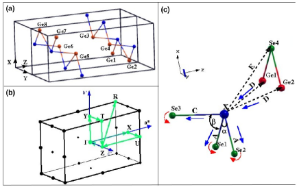
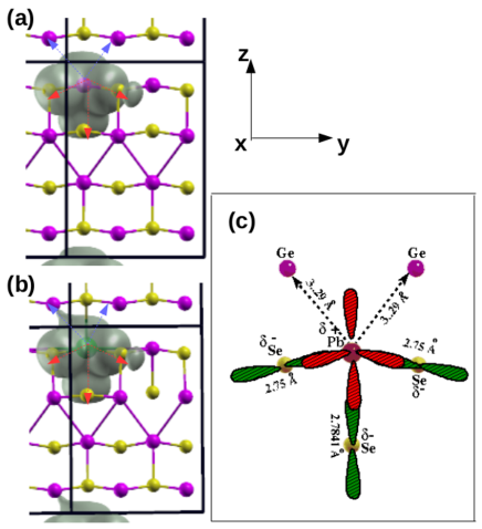
Fig.1(a) shows two units of orthorhombic unitcell of GeSe crystal. This crystal belongs to space group symmetry D Pcmn(62) and its lattice parameter c = 10.78 Å is larger than other two lattice constants a = 4.38 Å and b = 3.82 Å[13]. In the unit cell Ge/Se atoms are arranged in two adjacent double layers where each layer consists of two double corrugated planes. The coordination environment of the Ge atom is illustrated in Fig.1(c). It can be seen that two first nearest neighbour (fnn) Se atoms(Se1 and Se2) and second nearest neighbour (snn) Se atom (Se3) are situated at the comparable distances ( 2.56 Å) from the Ge atom. Whereas, third nearest neighbour (tnn) Se atom (Se4) and two fnn Ge atoms (Ge1 and Ge2) reside on the adjacent double layer with interatomic distances of 3.38 Å. Bond angles and formed by the atoms Se1-Ge-Se2 and Se3-Ge-Se1/Se2 are 95∘ and 90.8∘ respectively. In doped compounds Ge atoms are substituted by Pb atoms in the supercell structure of GeSe. In order to choose the substitutional sites for Pb doping, total SCF energy was compared of all the possible supercell structures of 0.25 doped GeSe which can be formed by substituting two Pb atoms at different Ge sites. This was minimum for the structure, where both the Pb atoms were situated maximally apart from each other. To keep this fact in mind Pb atoms were substituted in the supercell structure of GeSe (Fig.1(a)) at Ge1; at Ge1, and Ge5; at Ge1, Ge4, and Ge8 and at Ge3, Ge4, Ge7, and Ge8 for doping concentrations x = 0.125, 0.25, 0.375, and 0.5 respectively. And cohesive energy was calculated for all these structures which informed their stabilization in the orthorhombic phase. Similarly, structural relaxation of all the structures infers that mainly the coordination geometry is affected around the doped atom sites. The changes one of such site are marked by red and blue arrows in Fig.1(c). The distance of fnn and snn Se atoms with respect to the dopant atom (Pb) increases 0.2 Å whereas a quite small reduction of 0.05 Å is observed in the distance of tnn Se atom(Se4). The bond length of Ge1-Pb and Ge2-Pb decreases 0.1 Å which probably enhances the interaction between two adjacent double layers. Similarly, the bond angles , and are reduced by 3∘ which brings the fnn and snn Se atoms close to each other and thereby distorts each double layer locally. These changes in the coordination geometry around the dopant site have been compared in all the compositions at different substitutional sites. and found that the changes remain almost same in all the cases.
Next, we present results of Wannier functions to understand the bonding character in these compounds. Panel (a) of Fig.2 shows Wannier function of Ge-4px, 4py, and 4pz, where black dot represents bond center. These Wannier functions are elongated more towards the fnn Se atoms which is also reflected in the position of their bond center. This provides a slightly polar character to the covalent bonding in GeSe and could be the result of higher electronegativity of Se atom in comparison to Ge atom. Panel (b) of Fig.2 shows Wannier functions (Pb-6px, 6py, and 6pz) of dopant Pb atom where an additional shift can be seen in the position of bond center of the Pb Wannier functions towards the fnn Se atoms in comparison to the situation in GeSe compound. This is an indication of further enhancement of polar character of the covalent bonds at the Pb doapnt sites compared to the sites of Ge atom.
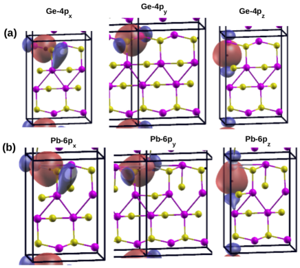
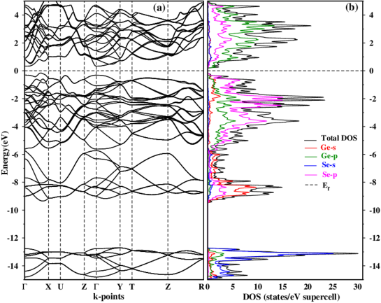
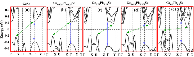
Fig.3(a) shows the band structure plot of GeSe. In the VB, bands are arranged in three separated energy regions, -14.47 to -12.48 eV; -9.32 to -5.52 eV; and -5.5 eV up to the Ef. Similarly the CB is also gaped from the VB with direct band gap(at the point) of 0.63 eV. However, possibility of an indirect band gap(0.49 eV) transition is also visible from the VB maximum near the X point to the CB minimum at the point. The bands are dispersive along the -Z and U-X directions mainly in the BE range Ef to -6.0 eV. These directions are perpendicular (kz) to the plane of the adjacent double layer(Fig.1(b)). This kz dispersion of the bands suggest a moderate hybridization between the adjacent double layers in the system. Similarly, the degenerate bands directed along the U-Z direction get splitted along the -X k-path which represents the k-direction same as the U-Z but lies on the adjacent double layer. In Fig.LABEL:gesedos(b) total density of states(DOS) of GeSe with different atomic contributions is plotted. Three demarcated regions in the DOS structure are consistent with the band picture. From partial DOS it is clear that the states are primarily composed of hybridized states between Se-4p and Ge-4p in the energy range -6.0 to 4.5 eV with an energy gap of 0.49 eV at Fermi level(Ef). In this energy window the VB and CB parts are dominant by Se-4p and Ge-4p states and they contribute 62.57% and 59.89% to the total DOS in the VB and CB regions respectively. On the other hand, lone pair states of Se-4s and Ge-4s reside deep in the BE in a narrow energy interval of -15 to -13 eV and -9.5 to -8.2 eV respectively. The lone pair states of Se-4s are quite separated from the 4p hybridized states of Se and Ge, while the Ge-4s states(7.4%) show a little admixture with these hybridized states. The Ge-4s states also contribute at the top of VB region which is defined as stereochemically active nature of the Ge-4s lone pair. These states have been found to involve in secondary bonding(s-s interaction) and played an important role in the formation of near Ef DOS in group IV-VI compounds as reported previously[36]. These results of band and DOS calculations on GeSe match fairly with previous report of Albanesi et. al.[14].
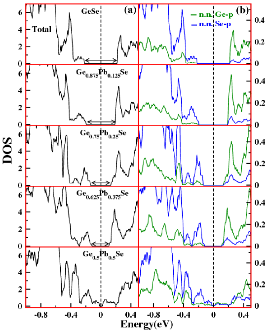
Next, we compared DOS of the Pb doped GeSe compounds and found interesting changes in the near Ef region of the DOS as depicted in Fig.4(a). Both the VB and CB edges gradually shift towards the Ef as a function of Pb doping. Apart from reduction in the energy gap, the states are also significantly enhanced just below and above the Ef which could be helpful in the increment of the photoabsorption in this system. As discussed previously, with Pb doping mainly the coordination environment affects around the doped sites. So, DOS composed of the fnn atoms of doped atom probably contribute primarily to the modified DOS in GeSe due to Pb doping. This view is supported by Fig.4(b), where DOS of the fnn Ge-4p and Se-4p orbitals of the doped atom are plotted in different doped compounds. As it is clear from this figure that these fnn Ge-4p and Se-4p states in each composition highly resemble with the corresponding total DOS and also show similar trend of the energy gap decrement at the Ef as a function of doping.
Band structure of different doped compounds informs that the bands close to Fermi level are mainly affected with doping. The near Ef band structure of various compositions are displayed in Fig.5(a)-(e), where it can be viewed that the lowest CB along the -Y direction gradually comes down towards the Ef with the Pb doping. While the top most VB along the -X and U-Z directions gradually goes up towards the Ef. This opposite moment of the CB and VB edges leads to a reduction in the indirect band gap (marked with green arrow). On the other hand CB edge at the point which involves in direct band gap show slight shift towards the higher BE for 0.125 case compared to the undoped case. In the next doping(0.25) the CB shifts slightly back to the lower BE then again comes back to the higher BE in 0.375 case. And in the 0.5 doped case it shows a significant shift towards the higher BE. Similarly, the VB edge at the point shows a small drift towards the higher BE from doping doping concentration x = 0.0 to 0.25 and opposite movement i. e. higher to lower BE for 0.375 to 0.5. Thus these changes in the CB and VB edges at the point provide an almost constant value of the direct band (marked with blue arrow) with Pb doping.
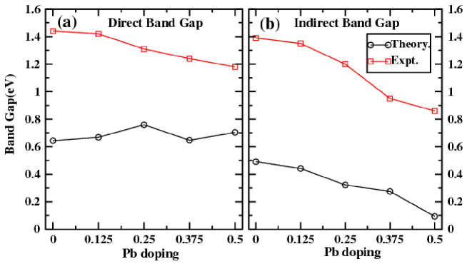
In Fig.6(a) and (b), we compared the calculated values of direct and indirect band gaps of compositions Ge1-xPbxSe (x = 0.0, 0.125, 0.25, 0.375 and 0.5) with experimental values of compositions Ge1-xPbxSe (x = 0.0, 0.1, 0.2, 0.3 and 0.4) respectively. The trend of indirect band gap reduction found in the calculation matches qualitatively to the experiment. There is an energy difference of 0.08 eV between both the values. On the other hand, the calculated value of direct band gap remains almost constant with doping, unlike the experimental value which shows slight decrement as a function of doping. This discrepancy could be arised from approximation used to formulate the many body electron interaction part in the DFT calculation. In this situation, the present first principles study could provide a ground for further experimental and theoretical investigations in this Pb doped GeSe and related systems to resolve the discrepancy of the energy band gap.
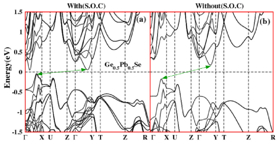
The effects of SOC are important in the elements which have a high atomic number(Z), like Pb. Because it is proportional to the atomic number of the elements (Z4). Therefore, the role of SOC effects are examined in the case of highest Pb concentration (0.5). Fig.7(a) and (b) show band structure of Ge0.5Pb0.5Se without and with inclusion of SOC effects respectively. Comparing the SOC results to non SOC case, a significant splitting can be viewed in the bands due to SOC, especially along the -X and -Y directions. Likewise, both the CB and VB edges move remarkably towards the Ef under the influence of SOC effects. This gives rise to lowering of the indirect band gap in SOC case in comparison to the non SOC case. These results signify the vital role of SOC effects in the modification of the electronic structure of Ge0.5Pb0.5Se. The important role of SOC effects in various binary and quaternary compounds of group IV-VI family, like Bi2Se3, BxSb1-xTexSe1-x[37] has also been discovered recently in the formation of non trivial topological surface states.
In order to figure out the reason behind the gradual shifting of the VB and CB edges, we calculated the charge density of Ge atom in GeSe and doped Pb atom in Ge0.875Pb0.125Se. These charge densities were calculated by using their s and p Wannier functions and results are displayed in Fig.8(a) and (b) respectively. In both the cases, the charge density covers the fnn Se atoms while the fnn Ge atoms are outside this coverage. In addition, bond center of the dopant Pb-6p Wannier functions lies close to its fnn Se atoms as clear from the Fig.2(b). This provides a positive character () to the Pb atom and a negative character () to the fnn Se atoms. Thus, doped site acts like a positive charge center and due to its electrostatic interaction it tries to pull all the bands towards the higher BE. The effect of this positive charge of the doped atom should be more to its nn atoms due to inverse square dependency of the Coulomb interaction with the distance from the source. Therefore, the fnn Ge-px/y orbitals pull down to the higher BE under the influence of Pb dopant. However, energy of the fnn Ge-pz orbital should not change appreciably because this orbital is lesser involved in the covalent bonding compared to the fnn Ge-px/y and thereby it readjusts itself according to the new environment. It could be possible due to one of the the fnn Ge-pz lobe( directing out of the fnn Ge-px/y plain) is more distant from the nn Se atoms. On the other hand, in the case of fnn Se-px/y orbitals the effect of charge at the dopant site is substantially screened by the bonding electron cloud which is resided close to these fnn Se atoms. Further, the electronic repulsion of these bonding electron cloud pushes the fnn Se-px/y orbitals to the lower BE. The same situation could also persists for the fnn Se-pz orbital but it is also oriented out of plain, like the fnn Ge-pz. So, there is possibility of readjustment of this orbital to reduce the repulsion of the bonding electronic cloud. As it is clear from the DOS plots(Fig.3(b)) that the modified DOS structure in the VB and CB region (in the vicinity of Ef) with Pb doping is mainly composed of the nn Se-p and Ge-p atoms of the doped atom. This informs that the bands present close to the Ef in the VB and CB region are dominant with the fnn Se-p and Ge-p atoms of the doped atom. Therefore, the shifting of the VB edge towards the lower BE along the U-X and -Y directions as a function of Pb doping is the result of electronic repulsion seen by the fnn Se-px/y orbitals. Similarly, shifting of the CB edge towards the higher BE along the -Y direction could be the outcome of electrostatic attraction exerted on the fnn Ge-px/y orbitals by the doped atoms. The VB edge shows a small shifting to higher BE energy at the point for doping x = 0.0 to 0.25. However, this VB edge moves slightly towards lower BE for compositions x= 0.375 and 0.5. In these highly doped systems, two Pb atoms are present in one of the double layers (at dopant site Ge1 and Ge5 in x = 0.375; Ge1/Ge2, Ge5/Ge7 in x = 0.5), unlike the cases of x = 0.125 and 0.25 doping. These atomic arrangements probably modify the bonding electron cloud at the doped atom site such that electronic repulsion overcomes the attractive electrostatic interaction of doped Pb cation () and thereby moves the fnn Se-pz bands to lower BE, like the Se-px/y bands. Furthermore, CB edge at the point which shows movment towards the Ef for doping values x = 0.0 to 0.125 shifts slightly in opposite direction (away from the Ef) for x = 0.25 and 0.5. This could be related to readjustment of the fnn Ge-pz orbital with respect to the fnn Ge-px/y orbitals.
4 Conclusion
We have presented a detail study of the electronic structure evolution of Ge1-xPbxSe, where x = 0.0, 0.125, 0.25, 0.375, and 0.5 using first principles method. The Se-p and Ge-p states are strongly hybridized in GeSe and a gap is observed in the DOS at Ef. This gap reduces systematically with simultaneous enhancement of the states in the near Ef region as a function of Pb doping. The doping mainly affects the coordination environment around the doped atom site as clear from the relaxed structures of the doped compounds. This result is consistent with the DOS results where we observe that the near Ef modified states are mainly composed of the fnn Se-p and Ge-p states. Similarly, in the band structure plots we found shifting of the VB and CB edges which gives rise to noticeable decrease in the indirect band in GeSe with Pb doping. This reduction of indirect band gap matches qualitatively with the experimental results. From Wannier functions it is revealed that the bond center of Pb-Se bond lies close to Se atom which gives rise to slight positive charge at the doped atom site. The electrostatic effect originating from these doped atoms tries to increase the BE of the fnn Ge-px/y orbitals. Whereas, bonding electron cloud centered at the fnn Se site screens the positive charge of the doped atom and reduces the energy of the fnn Se-px/y orbitals. Therefore, this electrostatic influence of the doped Pb atom could be the reason for shifting of the VB and CB edges and resulting indirect band gap reduction in Ge1-xPbxSe system. Our comprehensive study is helpful for further experimental and theoretical investigations of group IV-VI compounds in the context of controlling their properties with doping.
5 References
References
- [1] Hao Wei, Shangzhi Chen, Xinglong Ren, Bingjian Qian, Yanjie Su, Zhi Yang and Yafei Zhang, CrystEngComm , 14 (2012) 7408.
- [2] S.G.Hickey, C. Waurisch, B. Rellinghaus and A. Eychmuller, J. Am. Chem. Soc., 130, (2008), 14978.
- [3] W.J.Baumgardner, J. Choi, Y. Lim and T. Hanrath, J. Am. Chem. Soc., 132, (2010), 9519.
- [4] W. Ma, J. M. Luther, H. Zheng, Y. Wu and A. P. Alivisatos,Nano Lett, 9, (2009), 1699.
- [5] D. K. Smith, J. M. Luther, O. E. Semonin, A. J. Nozik and M. C. Beard ACS Nano, 5, (2011), 183.
- [6] Nagard N L, Levy-Clement C, Katty A and Lieth R M A Mater. Res. Bull., 25, (1990) 495.
- [7] Dandamudi P, Kozicki M N, Barnaby H J, Gonzalez-Velo Y, Mitkova M, Holbert K E, Ailavajhala M and Yu W IEEE Trans. Nucl. Sci., 60, (2013) 4257.
- [8] Nagard N L, Levy-Clement C, Katty A and Lieth R M A Mater. Res. Bull., 25, (1990) 495.
- [9] Shi Z, Xu G, McCann P J, Fang X M, Dai N, Felix C L, Bewley W W, Vurgaftman I and Meyer J R Appl. Phys. Lett., 6 (2000) 3688.
- [10] Boberl M, Heiss W, Schwarzl T, Wiesauer K and Springholz G,Appl. Phys. Lett., 82 (2003) 4065.
- [11] Guangqian Ding, Guoying Gao and Kailun Yao Sci. Rep., 5, (2015), 9567.
- [12] Gharsallah, M et al. Sci. Rep., 6, (2016), 26774.
- [13] Atushi Okazaki, Journal of the Physical society of Japan 13 (1958) 10.
- [14] L Makinistian and E Albanesi,J. Phys. Condens Matter 19 (2007) 186211.
- [15] L. M. Yu, A. Degiovanni, P. A. Thiry, J. Ghijsen and R. Caudano Phys.Rev.B 47 (1993) 16222.
- [16] H. C. Hsueh, H. Vass, S. J. Clark, G. J. Ackland and J. Crain Phys.Rev.B 51 (1995) 16750.
- [17] K. L. Bhatia, G. Parthasarathy, D. P. Gosain and E. S. R. Gopal, Phys.Rev.B 33 (1986) 1492.
- [18] P. B. Littlewood J. Phys. C: Solid St. Phys., 13 (1980) 4855.
- [19] Arthur Bienenstock,Journel of Non-Crystalline Solids 11 (1973) 447.
- [20] R. Dalven, Solid State Physics, edited by H. Ehrenreich, F. Seitz, and D. Turnbull(Academic Press, New York),
- [21] Eymard R. and Otto A. Phys. Rev. B 16 (1977) 1616.
- [22] P. Dziawa, B. J. Kowalski, K. Dybko, R. Buczko, A. Szczerbakow, M. Szot, E. Łusakowska, T. Balasubramanian, B. M.Wojek, M. H. Berntsen, O. Tjernberg and T. Story Nat. Matt., 11, (2012), 1023.
- [23] U. V. Waghmare, N. A. Spaldin, H. C. Kandpal, Ram Seshadri, Phys.Rev.B 67 (2003) 125111.
- [24] Ruchita R. Patel Thesis chapter 5 (2013) Optical Properties of GeSePbx (DVT) (x = 0, 0.1, 0.2, 0.3, 0.4) Single Crystals.
- [25] G. K. Solanki, K.D.Patel, N. N. Gosai and Ruchita R. Patel AIP Conf. Proc. 1447 (2012) 1063.
- [26] L. A. Wahab and H. H. Amer Mat. Chem. and Phys. 100 (2006) 430.
- [27] P Mishra, H Lohani, A K Kundu, R Patel, G K Solanki, Krishnakumar S R Menon and B R Sekhar Semi. Sci. and Tech. 30, (2015) 075001.
- [28] Giannozzi P et al. http://www.quantum-espresso.org.
- [29] Perdew J P,Burke K and Ernzerhof M Phys. Rev. Lett. 77 (1996) 3865.
- [30] Perdew J P and Wang y, Phys.Rev.B 45 (1992) 13244.
- [31] Perdew J P, Chevary J A, Vosko S H, Jackson K A, Pederson M R, Singh D J and Fiolhais C Phys.Rev. B 46 (1992) 6671.
- [32] Vanderbilt D Soft self-consistent pseudopotential in a generalized eigenvalue formalism Phys.Rev.B 41 (1990) 7892.
- [33] Pseudopotentials utilized in the present calculations were obtained from the quantum espresso pseudopotential library.
- [34] H. J. Monkhorst and J. D. Pack, Phys. Rev. B 13 (1976) 5188.
- [35] A. A. Mostofi, J. R. Yates, Y.-S. Lee, I. Souza, D. Vanderbilt and N. Marzari,Comput. Phys. Commun., 178 (2008) 685.
- [36] Andriy Zhugayevch and Vassilliy Lubchenko J. Chem. Phys. 133 (2010) 234504.
- [37] M. Z. Hasan and C. L. Kane Rev. Mod. Phys. 82 (2010) 3045.