[datatype=bibtex] \map[overwrite=true] \step[fieldset=url, null] \step[fieldset=doi, null] \step[fieldset=eprint, null]
SPAIC: A sub-W/Channel, 16-Channel General-Purpose Event-Based Analog Front-End with Dual-Mode Encoders ††thanks: This work received funding from the European Union’s H2020 research and innovation programme under the H2020 BeFerrosynaptic (871737), MeM-Scales (871371) projects.
Abstract
Low-power event-based analog front-ends (AFE) are a crucial component required to build efficient end-to-end neuromorphic processing systems for edge computing. Although several neuromorphic chips have been developed for implementing spiking neural networks (SNNs) and solving a wide range of sensory processing tasks, there are only a few general-purpose analog front-end devices that can be used to convert analog sensory signals into spikes and interfaced to neuromorphic processors. In this work, we present a novel, highly configurable analog front-end chip, denoted as “SPAIC” (signal-to-spike converter for analog AI computation), that offers a general-purpose dual-mode analog signal-to-spike encoding with delta modulation and pulse frequency modulation, with tunable frequency bands. The ASIC is designed in a 180 nm process. It supports and encodes a wide variety of signals spanning 4 orders of magnitude in frequency, and provides an event-based output that is compatible with existing neuromorphic processors. We validated the ASIC for its functions and present initial silicon measurement results characterizing the basic building blocks of the chip.
Index Terms:
Neuromorphic, Analog Front-End (AFE), Encoder, Spiking Neural Network (SNN)I Introduction
Spiking Neural Networks (SNNs) represent a powerful low-power event-based processing computing paradigm for processing streaming data on the edge [1].
To best exploit this novel emerging computing paradigm and build a robust end-to-end SNN sensory processing pipeline, designing efficient event-based analog front-ends is paramount. Fig. 1 illustrates such an end-to-end pipeline. There are various methods of encoding analog signals to spikes [2, 3]. On the hardware front, several analog-to-spike encoders have been developed and demonstrated on silicon, either using Delta Modulation (DM) schemes [4], thereby encoding the temporal changes in the original signal with spike timing, or with Pulse-Frequency Modulation (PFM) schemes [5, 6, 7], thereby encoding the amplitude of the signal with spike rates. However, these encoders were always optimized for a specific application and for the corresponding frequency bands.
To the best of our knowledge, no general-purpose solution has been proposed to allow exploration and prototyping with existing SNN neuromorphic computing platforms.

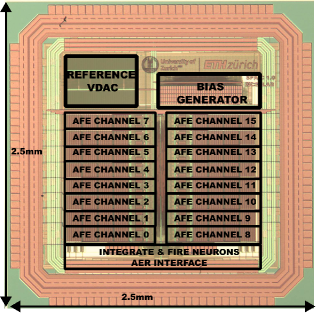
In this work, we present a highly configurable analog front-end ASIC, denoted as “SPAIC” (signal to spike converter for analog AI computation), which is compatible with existing neuromorphic processors [8, 9, 10, 11, 12], and which offers a general-purpose dual-mode (DM and PFM) analog-to-spike encoding with tunable frequency bands (see Fig. 2 for the chip micrograph).
II ASIC architecture
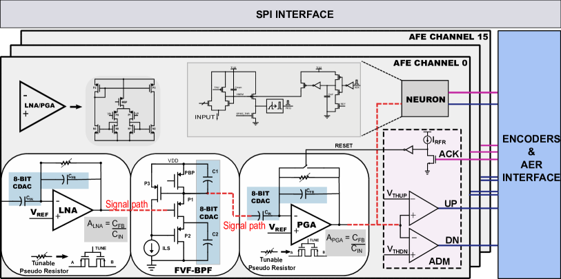
SPAIC comprises 16 identical analog channels feeding a common Address Event Representation (AER) interface as shown in Fig. 3. Each channel has four stages: a low noise amplifier section (LNA), a fourth-order flipped voltage follower (FVF) bandpass filter, a programmable gain stage (PGA), and the encoding stage. The LNA amplifies weak signals with tunable gain of 0 to 24dB. The FVF BPF filters the amplified signal with a tunable center frequency and Q [13]. The PGA further amplifies the filtered signal with a tunable gain up to 24dB. The amplified signal is then split in two mutually exclusive paths where either the asynchronous delta modulator encodes the temporal derivative of the amplified signal, or the integrate and fire neuron [14] is enabled and the signal is encoded as a pulse-frequency-modulated spike train. All configurations to the chip are provided in three ways: a configurable on-chip bias generator that generates the necessary bias currents for all circuits in the analog front-end, an 8-bit capacitor DAC (CDAC) to tune the filter parameters and a voltage DAC (VDAC) to set the UP and DN thresholds for the Asynchronous Delta Modulator (ADM). All three of these DACs are configurable via Serial Peripheral Interface (SPI) protocol.
III Circuit implementation
The SPAIC ASIC was designed and fabricated in a bulk 180 nm technology node. The chip dimensions including the seal ring are 2.5 mm2.5 mm. The circuit implementation of the major building blocks is described hereafter.
III-A Low noise amplifiers
For modularity reasons, both amplifiers in the analog front-end (LNA and PGA) are built on the same Operational Tranconductance Amplifier (OTA) core with minor changes adapted for noise and power. The structure of the OTA is based on a well-known wide input range current-mirror-type transconductance amplifier [15]. The primary reason for this design choice was to accommodate for large input changes that may or may not be present depending on the input sensor. The amplifiers are operated in a closed loop as capacitive feedback amplifiers with a DC-Servo loop (DSL) implemented with tunable pseudo resistors as shown in Fig. 3. The capacitance ratio of the feedback to input capacitance determines the overall closed-loop gain. This gain configuration is implemented as a 4-bit binary weighted capacitance DAC, leading to 16 distinct gain values. The gains as well as the noise performance were validated on silicon and are described in Section IV.
III-B Flipped Voltage Follower-based bandpass filter
Every AFE channel has a 4th-order BPF with tunable center frequency and Q. The FVF-based filter topology shown in Fig. 3 helps achieve better noise performance due to the inherent current reuse present in the architecture.
The filter’s center frequency () is tunable with the on-chip bias generator. The capacitors of this filter are implemented as an 8-bit CDAC. By configuring and , the Q and the center frequency can be adjusted in a precise manner with a resolution of steps, as described in Eq. (1).
| (1) |
As each filter’s center frequency and Q are programmable, they can be configured as a parallel filter bank or as identical parallel electrode interface channels. The frequency response, when configured as a filter bank, measured from the functional silicon is shown in Fig. 6, Section IV.
III-C Asynchronous Delta Modulation encoder
The ADM is designed based on the foundation of a level-crossing ADC. The amplified and conditioned signal is compared with two known voltage thresholds (an up threshold and a down threshold) set by an on-chip voltage DAC. When the signal crosses the up threshold, an "UP" spike is generated and similarly, in the other direction a "DOWN" spike is generated when the signal goes below the set down threshold. The DACs were simulated running Monte Carlo analysis and the absolute accuracy (3) of the voltage thresholds was found to be 900 . The comparator used in this ADM was designed with hysteresis [16, 17] to avoid false triggering due to fluctuations in the signal path arriving at the input of the comparator.
III-D Pulse Frequency Modulation encoder
The PFM encoder was designed using a leaky integrate and fire neuron (LIF) circuit [14] which inherently encodes the amplitude of the input current into pulse frequency. Therefore, before being encoded into spikes, the input signal is half-wave rectified and converted into current by a wide-range transconductance amplifier. The output current of this amplifier flows into the input of the neuron which generates a spike when the input current crosses an externally set spiking threshold of the neuron.
IV Silicon validation and measurement results
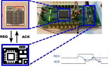
A custom evaluation board with a Teensy microcontroller was designed to evaluate the functionality of the ASIC. The setup is shown in Fig. 4. The microcontroller communicates with the ASIC and programs its internal registers via an SPI communication protocol. The two separate encoding paths are fully independent of each other and have their own AER circuitry. The AER circuitry operates based on a well-established four-phase hand-shaking mechanism described in Fig. 4 [18]. The asynchronous nature of the AER interface ensures sparse event-driven communication with other asynchronous devices.
The frequency response of the amplifiers and the noise power spectral density (Noise-PSD) measurement of the AFE are shown in Fig. 5. The plots show the noise PSD in the 1 Hz-1 kHz band, which is mainly dominated by flicker noise. The input-referred noise is 1.4 measured at the output of the first LNA.
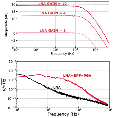
Fig 6 shows a measurement where the bias currents were programmed in octaves to obtain center frequencies spaced in octaves.
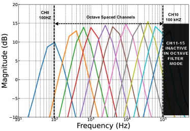
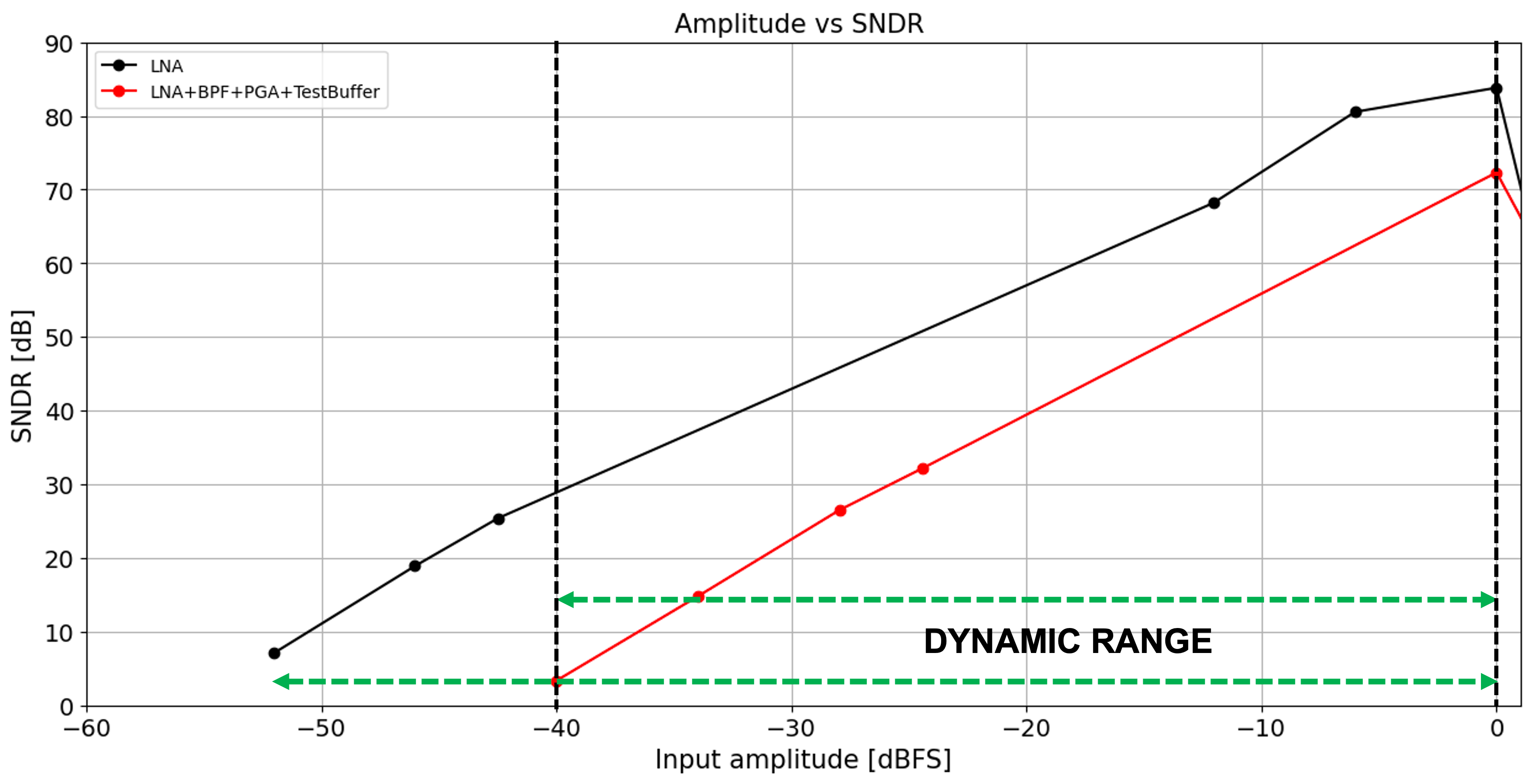
When the filter channels are octave-spaced, 11 channels can cover a range of 100 Hz-100 kHz. When used as identical channels, all 16 curves roughly overlap each other. The filter has a dynamic range superior to 40dB, however, reducing the gain of the first amplification stage helps to avoid distortion in the filtering stage. The silicon measurement of signal-to-noise and distortion ratio (SNDR) of a single AFE channel reveals a dynamic range of 42dB at the output of PGA as shown in Fig. 7.
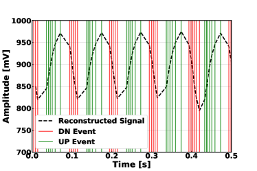
The encoding functionality of both ADM and PFM were measured on the silicon. A 100 Hz pure tone was encoded with ADM and the UP and DOWN events were recorded. To validate the encoding, the signal was reconstructed from the spikes and is shown in Fig. 8. A finer or coarser signal reconstruction can be achieved depending on the configured voltage thresholds. The final encoding accuracy is further determined by the input referred offset of the comparators.
Similarly, the functionality of the neuron as a PFM encoder was validated by physical measurement of its membrane potential in response to a 100Hz pure tone as shown in Fig. 9. The red trace in Fig. 9 shows the response to a 100mV input and blue trace to a 400mV input. The almost linear relationship of the spiking frequency to input amplitude shown in Fig. 10 confirms the intended functionality of the block.
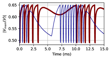
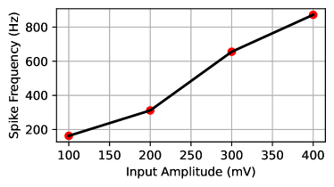
Table IV compares the performance of this work with similar event-based analog front-ends. This design can cover a programmable range from 100 Hz to 100 KHz.
ccccc
Technology [nm] 180 180 180 90
\hdottedline
Feature Analog to Analog to Analog to Analog to
Events Events Events Events
Channels 16 16 64x2 16
Bandwidth [Hz] 100-100K 100-5K 8-20K 75-5K
Power/Channel [nW] 800@100KHz 24 430 380
Normalized Power 11footnotemark: 1[nW] 532 88 821 1500
Input Referred Noise [] 1.4@LNA 8.3 30 32.5
Dynamic Range [dB] 55@LNA 40@IAF 55@BPF 45@LNA
40@PGA
Area/Channel [] 0.09 0.1 0.26 0.13
Functional Building LNA LNA LNA LNA
Blocks BPF BPF BPF BPF
PGA FWR PGA FWR
ADM IAF ADM LPF
OTA+AdExpI&F
Normalized to 5kHz using equation (8) in reference [4]
The AFE consumes about 800 nW with the channel processing at the highest frequency (100 kHz) enabled. All other lower-frequency channels consume proportionally lower power. The power consumption was normalized to 5kHz and the normalized power for SPAIC AFE is about 532 nW.
V Conclusions
In this paper, we proposed a highly configurable general-purpose signal-to-spike encoding ASIC with a dual-mode encoding scheme, designed and fabricated in 180 nm technology.
We demonstrated a generic signal conditioning and dual-way encoding scheme that one can pair with a spiking neural network to build an event-based neuromorphic sensing system. The design is comparable to the state-of-the-art in terms of dynamic range and silicon area and is better in terms of the operating range across a larger frequency range and noise performance.
Future work includes quantitatively benchmarking the encoding schemes with a few selected applications such as low-frequency biomedical signals to auditory signals and high-frequency ultrasonic signals and quantifying the normalized power consumption for any selected application.
This work represents a key enabler for building an end-to-end signal acquisition pipeline for edge computing nodes with spiking neural networks.
References
- [1] Chiara Bartolozzi, Giacomo Indiveri and Elisa Donati “Embodied neuromorphic intelligence” In Nature Communications 13.1024, 2022, pp. 1–14
- [2] Wenzhe Guo, Mohammed E. Fouda and Nabil Eltawil “Neural Coding in Spiking Neural Networks: A Comparative Study for Robust Neuromorphic Systems” In Frontiers in Neuroscience 15, 2021
- [3] Evelina Forno et al. “Spike encoding techniques for IoT time-varying signals benchmarked on a neuromorphic classification task” In Frontiers in Neuroscience 16, 2022
- [4] Minhao Yang, Chen-Han Chien, Tobias Delbruck and Shih-Chii Liu “A 0.5V 55W 64×2-channel binaural silicon cochlea for event-driven stereo-audio sensing” In 2016 IEEE International Solid-State Circuits Conference (ISSCC), 2016, pp. 388–389
- [5] F. Corradi and G. Indiveri “A Neuromorphic Event-based Neural Recording System for Smart Brain-Machine-Interfaces” In Biomedical Circuits and Systems, IEEE Transactions on 9.5, 2015, pp. 699–709
- [6] Minhao Yang et al. “A 1W voice activity detector using analog feature extraction and digital deep neural network” In 2018 IEEE International Solid - State Circuits Conference - (ISSCC), 2018, pp. 346–348
- [7] Komail Badami, Steven Lauwereins, Wannes Meert and Marian Verhelst “24.2 Context-aware hierarchical information-sensing in a 6W 90nm CMOS voice activity detector” In 2015 IEEE International Solid-State Circuits Conference - (ISSCC) Digest of Technical Papers, 2015, pp. 1–3
- [8] Saber Moradi, Ning Qiao, Fabio Stefanini and Giacomo Indiveri “A Scalable Multicore Architecture With Heterogeneous Memory Structures for Dynamic Neuromorphic Asynchronous Processors (DYNAPs)” In IEEE Transactions on Biomedical Circuits and Systems 12.1, 2018, pp. 106–122
- [9] Mike Davies et al. “Loihi: A Neuromorphic Manycore Processor with On-Chip Learning” In IEEE Micro 38.1, 2018, pp. 82–99
- [10] Charlotte Frenkel and Giacomo Indiveri “ReckOn: A 28 nm Sub-mm2 Task-Agnostic Spiking Recurrent Neural Network Processor Enabling On-Chip Learning over Second-Long Timescales” In 2022 IEEE International Solid-State Circuits Conference Digest of Technical Papers (ISSCC), 2022, pp. 468–470 IEEE
- [11] Christian Mayr, Sebastian Hoeppner and Steve Furber “Spinnaker 2: A 10 million core processor system for brain simulation and machine learning” In arXiv preprint arXiv:1911.02385, 2019
- [12] Charlotte Frenkel, Martin Lefebvre, Jean-Didier Legat and David Bol “A 0.086-mm2 12.7-pJ/SOP 64k-Synapse 256-Neuron Online-Learning Digital Spiking Neuromorphic Processor in 28-nm CMOS” In IEEE Transactions on Biomedical Circuits and Systems 13.1 IEEE, 2019, pp. 145–158
- [13] Yang Xu, Jason Muhlestein and Un-Ku Moon “A 0.65mW 20MHz 5th-order low-pass filter with +28.8dBm IIP3 using source follower coupling” In 2017 IEEE Custom Integrated Circuits Conference (CICC), 2017, pp. 1–4
- [14] Arianna Rubino et al. “Ultra-Low-Power FDSOI Neural Circuits for Extreme-Edge Neuromorphic Intelligence” In IEEE Transactions on Circuits and Systems I: Regular Papers 68.1, 2021, pp. 45–56
- [15] R.R. Harrison “A low-power, low-noise CMOS amplifier for neural recording applications” In 2002 IEEE International Symposium on Circuits and Systems. Proceedings (Cat. No.02CH37353) 5, 2002, pp. V–V
- [16] D.J. Allstot “A precision variable-supply CMOS comparator” In IEEE Journal of Solid-State Circuits 17.6, 1982, pp. 1080–1087
- [17] P.E. Allen and D.R. Holberg “CMOS Analog Circuit Design”, The Oxford Series in Electrical and Computer Engineering OUP USA, 2011
- [18] J. Lazzaro et al. “Silicon auditory processors as computer peripherals” In IEEE Transactions on Neural Networks 4, 1993, pp. 523–528