A Review of Techniques for Ageing Detection and Monitoring on Embedded Systems
Abstract
Embedded digital devices, such as Field-Programmable Gate Arrays (FPGAs) and Systems on Chip (SoCs), are increasingly used in dependable or safety-critical systems. These commodity devices are subject to notable hardware ageing, which makes failures likely when used for an extended time. It is of vital importance to understand ageing processes and to detect hardware degradations early. In this survey, we describe the fundamental ageing mechanisms and review the main techniques for detecting ageing in FPGAs, microcontrollers, SoCs, and power supplies. The main goal of this work is to facilitate future research efforts in this field by presenting all main approaches in an organized way.
I Introduction
The ubiquity of embedded devices keeps on growing, driven by increasing chip integration levels and computing capacity as well as by reduced prices and power consumption. Applications ranging from consumer electronics and IoT gadgets to space missions, nuclear power plants, and particle accelerators involve embedded sensors and actuators. Many deployments challenge the lifetime of these devices by employing unhardened Commercial Off-The-Shelf (COTS) components, by extending mission times over the guaranteed life span, or by harsh operational conditions.
Hardware ageing is a growing problem for embedded devices with a key role in dependable or safety-critical applications. The impact of physical degradation increases for new highly integrated technologies [1]. A particular problem for many Integrated Circuits (ICs) in long-term deployments is transistor degradations, namely Bias Temperature Instability (BTI), Hot-Carrier Injection (HCI), and Time-Dependent Dielectric Breakdown (TDDB). Their predominant consequence is an increment of the transistor’s threshold voltage, which reduces the maximum switching speed of Complementary Metal-Oxide-Semiconductor (CMOS) logic circuits. This reduction potentially affects critical paths in digital applications or the performance of other devices.
Microcontrollers and System-on-Chips (SoCs) are the most prominent digital components in embedded applications, as they can perform complex tasks at low prices and low power capabilities. They can even run operating systems with full-featured IPv6 software stacks [2], which makes them a popular central component in embedded scenarios. Field Programmable Gate Arrays (FPGAs) are likewise widely deployed, owing to their high level of flexibility as compared to Application Specific Integrated Circuits (ASICs). Serving even demands from Artificial Intelligence (AI) on the Adaptive Compute Acceleration Platforms (ACAPs), which combine CPU cores, programmable logic, and AI inference acceleration, FPGAs open their way into the edge-computing and high-end edge IoT markets. New radio frequency features via RFSoC (Radio Frequency System on Chip) enable them to acquire RF signals directly on the chip via integrated ADCs, which makes FPGAs even more competitive in RF deployments. A prominent use case from accelerator physics operates FPGA hardware as part of mission-critical systems for low-level radio frequency control loops and beam diagnostics.
Embedded devices are composed of a wide variety of components, most of which have been individually analysed. To assess the reliability of embedded systems, a comprehensive approach to detecting and monitoring ageing of the entire hardware boards is missing. In this paper, we survey the current state-of-the-art research on studying hardware ageing effects of common components found in embedded systems. We focus on techniques to detect and monitor degradation processes with the aim of predicting failures.
In the remainder of this paper, we give an overview of the ageing mechanisms that affect embedded systems in Section II. This includes the degradation of transistors, interconnects, and passive components. Section III overviews the reviewed literature and introduces relevant taxonomies. Section IV, Section V, and Section VI describe in detail ageing detection and monitoring strategies for FPGAs, microcontrollers and SoCs, and power supplies, respectively. The paper concludes in Section VII with an outlook on future research directions.
II Ageing Mechanisms in Embedded Systems
A failure is a non-conformance to a defined performance criterion [3]. Dependable systems require reliability, which represents the system’s probability of being failure-free for a given period of time (i.e., it performs under specified limits). Design requirements usually specify failure rates , which are the probability of failing at a certain point in time.
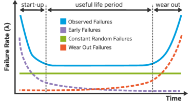
A component’s failure rate varies during its lifespan and is typically described using the bathtub distribution (see Fig. 2). The observed failures over time are the sum of three overlapping distributions, namely early failures, constant random failures, and wear-out failures, which lead to three distinct curve regions. The first region is the start-up, also known as burn-in, in which the failure rate decreases over time. Failures in this region are mostly due to manufacturing problems. The middle region is the useful life period, in which failures occur randomly at a constant rate. The last part of the distribution is the wear-out period. The acceleration of degradation mechanisms (e.g., component ageing) causes an increasing failure rate in this region.
Components of embedded systems suffer degradation during their lifetime. Ageing processes are gradual, and their results are usually only noticeable in the long term. Very Large-Scale Integration (VLSI) chips are subject to multiple wear-out or degradation processes that shift their parameters away from specification, eventually resulting in system failures [4]. Ageing in chips has two sources: transistor and interconnect degradation. In addition, passive components such as capacitors and inductors age as well [5] and cause problems in voltage regulation circuits [6].
In this section, we describe the most relevant ageing mechanisms affecting the core components which compose devices commonly found in embedded systems.
II-A Ageing of Transistors
Silicon manufacturers face more challenges with new miniaturized transistor technologies. The reduction in size has not been proportionally followed by a reduction in operation voltage, resulting in stronger electric fields applied to the devices. In the following sections, we describe the main ageing mechanisms that impact Metal-Oxide-Semiconductor Field-Effect Transistors (MOSFETs), which are the base for all current CMOS technologies.
II-A1 Bias Temperature Instability (BTI)
BTI is an ageing mechanism [7, 8] most prevalent on p-channel MOSFETs, where it is Negative BTI (NBTI). Since the introduction of high-k/metal transistors, BTI effects are also considerable on n-channel MOSFETs, affected by Positive BTI (PBTI) [9]. The consequences of NBTI are an increase in the threshold voltage and a degradation of the carrier mobility, drain current, and transconductance.
Although the mechanism is not fully understood, the main cause for NBTI is attributed to the creation of traps in the oxide-substrate () interface and charges in the oxide. The most prevalent model is the Reaction-Diffusion (R–D) [10, 11]. It proposes that low-energy bonds on the interface break due to the presence of applied electric field and high temperature, with a linear relation to the stress time (i.e., reaction). Afterwards, positive charges ( or trapped holes) diffuse into the gate oxide with a time dependence (where usually ), leaving dangling bonds or interface traps behind [7]. The accumulation of positive charges in the oxide opposes the applied electric field, thus inducing a variation in the threshold voltage of the transistor (). This reduces the maximum switching speed of the device.
BTI has a recovery phase: once the gate bias is removed, the diffused charges return to the interface and anneal the traps. Although this process reduces , it is not completely clear whether the recovery is full: some evidence indicates the possibility of a 100% of recovery [12], while other studies propose the existence of both permanent and reversible degradation components [13]. As the mechanism is partly governed by a diffusion process, its duration highly relates to the operating temperature. Owing to the recovery phase, degradation depends on the stress duty cycle; thus, continuous stress (DC) is much more severe than non-continuous (AC) [14].
II-A2 Hot Carrier Injection (HCI)
As a lateral electric field between drain and source is applied to a transistor, carriers (electrons or holes) gain kinetic energy, becoming “hot“ when their energy is significantly larger than the one of the lattices at thermal equilibrium [15]. Due to their high energy, some carriers are able to surpass the potential barrier of the gate oxide, injecting themselves into the dielectric or causing damage to the interface. This has similar symptoms as BTI, namely: increase of the threshold voltage , decreased carrier mobility, and a reduction in the transconductance in the transistor saturation region [16, 17, 18]. The impact of HCI is directly proportional to the frequency at which the device is switched, as hot carriers are generated during the transistor’s transitions. Unlike BTI, HCI presents no recovery phase when the stress is removed.
II-A3 Time-Dependent Dielectric Breakdown (TDDB)
TDDB is a gradual and irreversible degradation mechanism in the gate oxide of transistors. Defects accumulated in the layer allow an increase in gate leakage current, thus slowing down the transistor switching frequency. Nigam et al. [19] describe three stages of the degradation process, illustrated in Fig. 3: (i) Defect generation starts when a large electric field is applied to the gate dielectric. As the defect density is still not critical, there is still no current. (ii) With continued stress, more defects are generated and start to overlap, producing a soft breakdown. Now traps form a resistive path between the gate and the channel, increasing the leakage current and reducing the device switching speed. (iii) Due to the thermal damage caused by the leakage current, more traps form a wider and less resistive path. This increases the gate current even more, which leads to a thermal runaway that completely breaks the dielectric layer. At this point, the transistor structure is destroyed, and the device is unusable.

II-A4 Radiation-Induced Trapped Charges
When high-energy photons or charged particles interact with a material, they can cause ionization. Total Ionizing Dose (TID) denotes the total amount of transferred energy from ionizing particles to the material. As a consequence, semiconductors are vulnerable to photon-induced ionization damage via a process that generates two types of trapped charge: (i) oxide-trapped charges and (ii) interface traps [20]. Trapped charges accumulate over time and modify the transistor characteristics. The effect of radiation has been studied in many components commonly found in embedded systems: signal propagation changes within ICs [21], impact on voltage regulators [22], System-On-Chips and microcontrollers [23, 24, 25].
The trap generation process initiates when an ionizing particle impacts the gate oxide material of the transistor, transferring part of its kinetic energy. A number of electron-hole pairs are generated, proportional to the material activation energy and density [26]. Some pairs are annihilated through recombination, which is a function of the applied electric field [27], but some escape this process. A fraction of the remaining holes may fall into deep traps in the oxide or near the interface, forming the trapped positive charges. Other holes react with hydrogen-containing defects in the interface, generating interface traps.
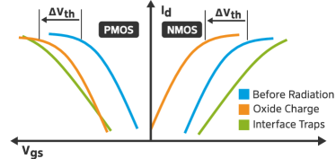
Oxide traps modify the DC characteristics of CMOS circuits, similarly to BTI, as depicted in Fig. 4. The most prominent effect is a negative shift in the drain current for a given gate-source voltage on P-MOS and N-MOS. In the first one, the absolute value of increases while the drain current is reduced. The latter one suffers a reduction of , with an increase of the drive current, potentially causing a latch-up (i.e., the transistor always conducts). Interface traps affect the recombination rates of carriers and their mobility through the channel. As the trapping and de-trapping of charges at the interface depend on the applied bias voltage, when these traps build up, they generate an increase in the sub-threshold swing of CMOS devices. The consequence is that the vs. response is stretched out, as shown in Fig. 4.
II-B Ageing of Interconnects
II-B1 Electromigration
To keep up with Moore’s Law [28], manufacturers constantly increase levels of integration. One way to integrate more devices is to reduce the width of the wires interconnecting them. This optimization comes at a cost: the smaller the conducting area, the higher the current density. Increasing current density entails a higher atomic diffusion phenomenon called electromigration. In the presence of high current densities, the strong momentum transfers from electrons to the conductor atoms to cause an atomic diffusion in the direction of the electron flow [29]. The force of the electronic wind causes atoms to deplete “up wind“ and accumulate “down wind“, until they create an electrical short- or open-circuit, rendering ICs unusable. Black [30] proposed to model the Median Time to Failure (MTF) in hours as Eq. 1, where is a constant, is the current density, is the activation energy for diffusion, is the Boltzmann constant, and is the temperature in Kelvin.
| (1) |
II-C Ageing of Passive Components
II-C1 Capacitors
Even though it is well known that electrolytic capacitors wear out with time [5], they are widely used in many embedded applications, from filtering signals to suppressing voltage ripples. As digital circuits lower their operating voltage, they become more susceptible to noise and require functioning capacitors over the whole deployment time. Most of the models representing real capacitors in electrical circuits describe an Equivalent Series Resistance (ESR), which causes energy dissipation as heat. Although ideally the ESR value is negligible, changes have been observed over time when the component is exposed to high temperatures [31]. The vaporization of the capacitor electrolyte through the encapsulation seal increases the ESR. As vaporization depends on the internal temperature and the ESR dissipates heat, it acts in positive feedback degrading the capacitor parameters.
II-C2 Inductors
Inductors are commonly employed to build analog filters and power supplies. Magnetic cores are usually inserted inside the coils to increase inductance. Depending on their composition and geometry, ferromagnetic cores generate energy losses due to eddy currents in the material induced by the fluctuating magnetic field. Indeed, according to Faraday’s law of induction, in the presence of a changing magnetic flux in an enclosed path, an opposite electromotive force is induced. This force will be proportional to the rate of change of the flux Eq. 2. The electric flux crossing a surface (bounded by a path ) can be expressed as Eq. 3, where is the magnetic field. The induced relates to the generated electric field over the closed path , as shown in Eq. 4. Finally, as shown in Eq. 5, the varying magnetic field in the enclosed inductor core will induce an electric field in the ferromagnetic material. Whenever the material of the core is conducting, a current density will appear on it.
| (2) | ||||
| (3) | ||||
| (4) | ||||
| (5) |
The power dissipation of the eddy currents depends on the induced electric field on the core and its resistivity. Inductor cores can undergo a degradation process when constantly exposed to elevated temperatures for long periods of time, which changes the material resistivity. This increases core losses [6] and contributes to further elevating the temperature.
III Surveying Ageing Detection Techniques
A defect is an unintended deviation of a component material, with continuous and physical nature and effects [32]. Defects originate either from manufacturing imperfections or from ageing during service. Defective behaviour can be abstracted to faults when modelled according to the circuit structure. For instance, a transistor threshold voltage degradation (i.e., a physical variation) can be modelled as a delay fault on a combinational circuit. When the system state or its environment triggers a fault, an error occurs. This may, in turn, cause a malfunction or complete failure.
The variety of potential defects of electronic components (see Section II) evidences the need for health assessment of embedded hardware. Prognostics and remaining-useful-life estimations [33] can leverage this information. The evolution of physical ageing processes can indirectly be assessed during operation by observing deviations of device parameters, either by directly comparing against pre-established profiles or with sophisticated anomaly detection techniques [34].
III-A Surveying Methodology
The research for the presented literature comprised consulting of various notable scientific databases (IEEE, ACM, and Google Scholar) while limiting the results with keywords including ag(e)ing, degradation, failure, monitoring, and the components of interest: FPGA, microcontroller, system on chip, and power supply. We excluded, however, board-level mechanical wear-out effects, such as broken interconnects or the degradation of solder joints. Upon the initial searches, we followed the related work referenced by the results. References were selected with the objective of maximizing the variety of detection and monitoring approaches. This literature compendium includes both methods originally designed to assess the system health status while on service and methods which have been employed to study the impact of ageing processes on devices under controlled environments.
III-B Classification of Tests
Tests of embedded system components can be classified according to whether the system can perform them autonomously: either self-tests or external tests. Moreover, depending on whether self-tests run on dedicated hardware in the component or their functionalities are controlled by software, they can be further classified as built-in self-tests or software-based self-tests.
III-B1 External Test
External tests usually involve automatic testing equipment and extra hardware or tools. These tests are typically required whenever observed magnitudes need special detection techniques or sensors not present in the system (e.g., radiated electromagnetic emissions). External tests are most times much more expensive and cumbersome to carry out than self-tests. For this reason, they are mainly reserved for in-lab evaluations under controlled environments or post-mortem analysis, and are rarely deployed in the field.
III-B2 Self-Test
Self-tests leverage the existing capabilities of the devices under test to evaluate their own functionality, thus avoiding extra equipment. Depending on the measurement methodology, a self-test can be (i) online, or (ii) offline. The former runs in parallel to the applications and is useful to monitor systems which cannot afford downtime. The latter is performed outside the device service schedule (e.g., during boot or maintenance periods).
Built-In Self-Test (BIST) reuses built-in hardware features to test a system [35, 36]. The technique proposes a hierarchical top-down architecture where all components expose a BIST interface to the upper level, thus abstracting the specifics of each device. The whole system can be tested by sending a BIST control signal to the components on each hierarchy. They perform the specific tests and return the results to the upper level. BIST requires three basic hardware blocks: (i) a pattern generator produces the test stimuli injected to the circuit under test, (ii) a response analyser receives responses and decides the test result, (iii) a test controller activates the test and analyses the responses from underlying levels. As BIST requires extra hardware logic, it may not be suitable for extremely constrained embedded systems, with limited area or when COTS devices without test hardware are used.
Software-Based Self-Test (SBST) is a nonintrusive type of test that utilizes software and existing hardware resources to verify the correct functionality of a device [37]. Unlike BIST, this approach requires no dedicated test hardware, as the pattern generation and response analysis are performed on software. Although SBST has been widely used to self-test microprocessor cores [38], hardware peripherals or even components within the embedded system can potentially be tested with the same principle. By reusing the processing power and integrated hardware (e.g., analog-to-digital and digital-to-analog converters), on-board microcontrollers can potentially perform test routines on themselves and on other attached components without external equipment [39].
III-C Overview of the Results
Considering the criteria described in Section III-A and the taxonomy introduced in Section III-B, relevant literature has been selected, reviewed and classified. Table I summarizes the studied related work, which is described and discussed in detail in the following sections. Approaches are organized by component: FPGA, MicroController Units (MCU) and SoC, and Low Drop-Out (LDO) and Switching-Mode Power Supply (SMPS). Contributions are further grouped according to their sensing principle. For each of the publications, it is indicated whether the technique was developed as an online or offline self-test or as an external test, and whether accelerated ageing was performed during its evaluation. At first glance, Table I reveals that most of the literature focusing on FPGAs proposes self-test approaches, while related work on MCUs, SoCs and power supplies usually rely on the usage of external equipment.
| Component | Sensing Principle | Ref. | Self-Test | Ext. Test | Accel. Ageing | ||
| Online | Offline | ||||||
|
FPGA
(see Section IV) |
Ring Oscillator | [40] | \faCheck | ||||
| [41] | \faCheck | \faCheck | |||||
| [42] | \faCheck | \faCheck | |||||
| [43] | \faCheck | ||||||
| [44] | \faCheck | ||||||
| [45] | \faCheck | ||||||
| [46] | \faCheck | ||||||
| [47] | \faCheck | \faCheck | |||||
| [48] | \faCheck | \faCheck | |||||
| [49] | \faCheck | \faCheck | |||||
| [50] | \faCheck | \faCheck | |||||
| [51] | \faCheck | ||||||
| [52] | \faCheck | \faCheck | |||||
| Shadow Register | [53] | \faCheck | |||||
| [54] | \faCheck | ||||||
| [55] | \faCheck | ||||||
| [56] | \faCheck | ||||||
| [57] | \faCheck | ||||||
| [58] | \faCheck | ||||||
| [59] | \faCheck | ||||||
| [60] | \faCheck | ||||||
| [61] | \faCheck | ||||||
| [62] | \faCheck | ||||||
| Transition Probability | [4] | \faCheck | |||||
| [63] | \faCheck | \faCheck | |||||
| [64] | \faCheck | \faCheck | |||||
|
MCU & SoC
(see Section V) |
SRAM Pattern | [65] | \faCheck | \faCheck | |||
| [66] | \faCheck | \faCheck | |||||
| [67] | \faCheck | \faCheck | |||||
| Time Window Violation | [68] | \faCheck | \faCheck | ||||
| EM Charact. | [69] | \faCheck | \faCheck | ||||
| [70] | \faCheck | \faCheck | |||||
| LDO PSRR | [71] | \faCheck | \faCheck | ||||
| [72] | \faCheck | ||||||
|
Power Supply
(see Section VI) |
SMPS | Equivalent Series Resistance | [73] | \faCheck | |||
| [74] | \faCheck | \faCheck | |||||
| [75] | \faCheck | \faCheck | |||||
| [6] | \faCheck | \faCheck | |||||
| EM Charact. | [76] | \faCheck | \faCheck | ||||
| [6] | \faCheck | \faCheck | |||||
| LDO | PSRR | [77] | \faCheck | \faCheck | |||
| [78] | \faCheck | \faCheck | |||||
| EM Charact. | [79] | \faCheck | \faCheck | ||||
IV Ageing Detection on FPGAs
FPGAs are programmable hardware devices that provide great flexibility, in-field updates, and rapid prototyping of digital designs. The majority of FPGA applications require high-speed processing, including digital filters and control loops with strict low latency requirements. SRAM-based FPGAs are the most popular in the market and use volatile memory to store their configuration. These devices present a regular structure of configurable logic blocks and programmable switch matrices that allow mapping logic functions.
FPGAs face reliability challenges as their transistor-based circuits are affected by ageing mechanisms. BTI and HCI increase signal propagation delays [52]. With the gradual decay of delays in the signals, critical paths of digital applications may change and even reach values out of specification.
Given their general purpose nature, and unlike ASICs, manufacturers cannot know beforehand what functionality will be synthesized on the FPGA chip, hindering the implementation of precautionary measures to cope with circuit degradation (e.g., guard-bands). This situation moves the issue of monitoring ageing processes to the application developers, who know the tolerances of signal propagation times.
IV-A Ring Oscillator
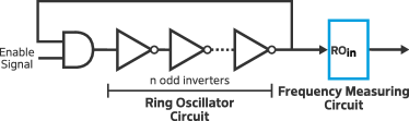
The flexibility of FPGAs enables implementing monitoring techniques directly on the programmable hardware. One of the most common approaches to measuring digital signal propagation time is Ring Oscillators (ROs), consisting of an odd number of inverters connected in a ring. RO-based sensors are usually composed of a RO and a frequency-measuring circuit (see Fig. 5). The frequency at the output of a RO depends on the inverters’ propagation time and the number of gates , as shown in Eq. 6.
| (6) |
Zick et al. [40] proposed an online sensing method to measure variations in physical parameters. By using an enhanced RO, an efficient counter, and control logic, the authors developed a compact sensor requiring only 8 Look-Up Tables (LUTs). A residue number system ring counter was implemented, as it requires fewer resources than a binary counter. The temperature sensitivity of the RO was increased to detect hotspots on the chip. RO sensors were placed regularly on a hexagonal tessellation all over the FPGA, together with a softcore, a timer, and a UART. The authors measured propagation times and indirectly estimated a transistor current leakage profile, localized dynamic power usage and temperature.
Sedcole et al. [44] placed ROs in a matrix configuration to measure within-die delay variability. The structure enabled encoding regions under test into columns and rows. In such a dense configuration, ROs should only be active for short periods of time to avoid heating neighbouring sensors. A single counter, timer, and unified control logic performed the measurements. Similarly, Maragos et al. [45] encoded the activation of ROs in addresses, which were used by an embedded Cortex-A53 CPU to control the process and collect the measurements via software. Pfeifer et al. characterized chip delays during design time [43] and analysed the limitations of 28 nm FPGAs [42] with ROs. To measure the oscillations, they implemented a method based on Block RAM (BRAM), which was later formalized in an approach called “Reliability-on-Chip“ [41]. The approach requires a true-dual-port BRAM on the chip to undersample the oscillators’ outputs and a softcore to read the signal streams for calculating the delays.
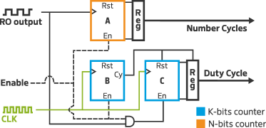
Naouss et al. proposed [47] a test bench to self-characterize the delay of LUTs. Their design allows injecting stress signals to the Circuit Under Test (CUT) to produce accelerated ageing. This feature was later used to independently study BTI [48] and HCI [49] impact by using different stress signals. The implemented frequency measuring circuit consisted of three asynchronous counters (one of N bits and two of K bits) and a clock reference. This circuit (see Fig. 6) allowed counting the number of cycles in a given period of time as well as the duty cycle of the signal. An enable signal activated the counters and controlled the counting window. Counter A registered the number of cycles of the RO output signal, which was used to calculate the oscillation frequency. Counter B counted the number of clock cycles during the active time of the RO signal, from which the duty cycle was calculated. Measuring the signal duty cycle allowed for studying the impact of ageing on the rising and falling times.
ROs have been employed in external test as well [50, 51, 52, 46]. Ahmed et al. [50] used performance degradation to detect recycled FPGAs by exhaustively fingerprinting LUT delays. They synthesized ROs with routes configurable via an SRAM. External equipment was used to control the test logic and read out the frequency of each oscillator. Ruffoni et al. [51] focused on measuring delays of the internal FPGA wires. Two ROs were used, where one included the wire structure under test. By comparing oscillation frequencies, the delay of the wire was derived. Although the authors employed external equipment, they argued that the method could potentially be carried out entirely on the device. Bruguier et al. [46] proposed a non-invasive method to characterize FPGAs performance, analysing the spectra of electromagnetic radiation caused by the ROs. A similar measurement approach was used by Amouri et al. [52] to explore the impact of elevated temperatures and voltages on the performance degradation of FPGAs.
Discussion
RO sensors are relatively easy to implement and very versatile. They can be tuned to indirectly measure magnitudes other than propagation delay [40]. Although the main sensing principle among authors is similar, literature presents multiple approaches to placing the sensors and counting the frequency. A trade-off exists with RO sensors: longer ring chains cover more area and require fewer measurement circuits but decrease sensor resolution. Care should be taken to avoid overheating the die or stress power rails by using too few stages in the rings, as this results in unrealistic measurements [43]. A downside of ROs is that they measure delays of the FPGA resources that form the ring and not of the synthesized circuits, which may differ depending on the position and routing. Other techniques, like the ones described in the following sections, measure delays of the existing combinational logic instead.
IV-B Shadow Register
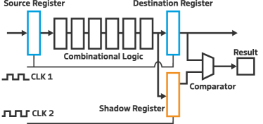
The usage of Shadow Registers (SRs) is a well-studied technique for delay characterization and degradation monitoring. Sensors are usually placed at the end of critical combinational paths, in parallel to a destination register, to detect late transitions.
Li et al. [56], Valdés et al. [55], and Leong et al. [53] proposed to place a SR after the CUT, clocked with a signal skewed from the destination register (see Fig. 7). By comparing the latched value by both registers and controlling the phase difference, the delay of the CUT was determined. Li et al. used varied the phase difference in runtime to characterize the FPGA propagation delay and build a histogram. Leong et al. implemented an online ageing monitoring sensor, which detected when the propagation delay was higher than a designed threshold. Valdés et al. included an on/off signal to their online sensor that would interrupt the clock signal. With it, the authors were able to decide the type of ageing mostly suffered by the sensor itself: static ageing (continuous monitoring) or dynamic ageing (periodic monitoring). The sensor functionality was initially tested by operating the test circuit under different power supply voltages, which induced a change in its signal propagation delays but did not affect the sensor. The sensor from Valdés et al. was then validated [54] by performing an accelerated ageing process on an FPGA. The authors reported no significant frequency variations of the clocks, on which the sensor reliability depended, after the burn-in process. Leong et al. tested their sensors by increasing the FPGA frequency and reducing the gap time.
Ghaderi et al. [58] proposed ageing monitors clocked by a single “sensor clock“, which set the maximum allowed slack for combinational signals of critical paths. By injecting the CUT signal and a shifted version of it to an XOR, a positive pulse was generated on each transition of the CUT. The XOR was latched by a Flip-Flop (FF), triggered by the sensor clock, detecting invalid transitions when the pulse occurred too late.
Pfeifer et al. [59] presented an online delay-fault detection technique for combinatorial circuits. The authors used the D FFs at the input of on-chip BRAMs as SRs, which map the signals to memory rows to be analysed at a later time. The interconnect introduced a fixed delay between the destination and the SR to control the sensor sensitivity, and an on-board CPU performed the signal comparison.
Wong et al. [61] presented a self-characterization method, with two registers around a combinational CUT, clocked in counter-phase. An XOR between the CUT output and the SR latched value produced the error signal. Transitions occurring after the first half of the test clock period were invalid. The authors leveraged on-chip clock generation to sweep the test clock frequency until the maximum was found. A BIST circuit for start-up tests was also proposed and optimized in [62], which stored test results of each region on the FPGAs RAM.
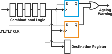
Amouri et al. [57] implemented an ageing sensor to detect late transitions of combinational paths on a Virtex-5 FPGA. The sensor, illustrated in Fig. 8, was composed of two edge-triggered D FFs clocked by the combinational output, with their inputs connected to the principal clock signal. Whenever an invalid change in the combinational signal occurred (i.e., during the active clock cycle), the sensor output was activated. Two FFs were used to detect rising and falling signal transitions. By the addition of independently configurable delay blocks on the combinational output signal and the clock signal, the authors could control the sensor sensitivity (i.e., how much time after the rising clock signal a change in the combinational output is detected). When sensitivity is configured to a negative value, the sensor is turned into an early warning monitor, which checks that the signal is stabilized at least by a given time before the clock rises. A great advantage of this method, in comparison to the previously described ones, is requiring no extra clock resources for the sensor.
A drawback of the previous approach was not quantitatively measuring the propagation delay but rather detecting transitions slower than a given threshold. Jiang et al. [60] proposed a similar architecture, but the inputs Q of both SRs were connected to a shadow clock signal, which had a phase shift relative to the main clock, to recover the capacity of measuring the CUT delay. By changing the phase angle between clocks and observing the sensor output, the propagation delay of the CUT could be derived, given the known clock frequency.
Discussion
Shadow registers appear more complex to implement and place than ROs, but the trade-off provides more versatility. These sensors enable measuring propagation delays of application-specific circuits (e.g., to characterize chips), as well as implementing late transition detectors. By focusing on checking that transitions occur within a given time window, this method can verify circuit functionality under different conditions and even be deployed for continuous monitoring of critical combinational paths.
IV-C Transition Probability
Propagation delay variations can be detected by observing the Transition Probability (TP) of a circuit [64, 63, 4]. Consider a combinatorial digital circuit with an output node . For each applied input combination, an output value is produced. The transition probability of z, denoted , is the probability of the state changing when the next input stimuli are applied [80] on the following clock cycle. As can only be zero and one, then is the probability of experiencing a transition between these states:
| (7) |
where and indicate the probability of undergoing the , transitions respectively. From [80], this probability can be calculated as the relative number of transitions that occurred in an interval of clock cycles, as . For instance, can be defined as:
| (8) |
If the probabilities are approximated by observing the transitions during a large number of clock cycles, we obtain:
| (9) |
then can be estimated by the relative amount of rising and falling edges of over a time interval .
Additionally, Ghosh et al. presented a theorem [80] which relates the output value probability with the input values probabilities on a combinatorial circuit. If the input signals have a probability distribution independent of time (i.e., they form a stationary process), then the output signal will also have this characteristic. This means that under this condition, the TP does not change in time.
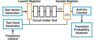
Wong et al. [64] estimated the maximum functioning frequency of an arbitrary circuit by measuring its output TP. With a careful selection of the input signals, they ensured a constant TP of the output under normal operating frequencies. They performed various measurements at increasing frequencies, up until the point where changes in the TP were observed. The change indicated that the circuit started failing, and the maximum frequency was reached. The proposed setup was implemented on a 65 nm Altera Cyclone III FPGA, as in Fig. 9. The CUT and registers were clocked from a test clock generator. On each clock cycle, the test vector generator injected input vectors, which propagated through the CUT generating an output . In addition, the sample register captured a sample from the CUT at a frequency . An asynchronous counter counted the transitions in over clock periods, later used to estimate in the TP analyser circuit. When is within the operational range, and no faults occur on the circuit, then and the transition probabilities . If is increased above the CUT propagation time, then will start to sample values of the previous cycle (i.e., ), thus changing .
The method proposed by Wong et al. was later applied in the study of circuit degradation under accelerated stress conditions by Stott et al. [63, 4]. The authors implemented multiple CUTs on a pair of Cyclone III FPGAs, which could be measured using the TP method and allowed to be electrically stressed by an input signal. Environmental stress with an ageing acceleration factor of was applied to the chips by means of elevated temperature and core voltage, which sped up the NBTI process. Additionally, the CUT was subjected to electrical stress by controlling its switching activity through the input signals, which triggered NBTI, TDDB, and HCI degradation mechanisms. Their experiments revealed a circuit speed reduction of up to 15% by the end of the test schedule and that stress conditions degraded stronger LUTs than interconnects. Moreover, the method was verified against a RO-based (see Section IV-A) frequency measurement.
Discussion
Measuring changes in the TP of a CUT’s output allows for detecting its maximum operational frequency. Unlike ROs (Section IV-A), this method measures the propagation delay of the FPGA using existing circuits, so the evaluation of the impact on the application is more direct. This technique has the advantage of being implementable with common resources and only requires a controllable clock signal. On the other hand, the method needs injecting precise test vectors, which depend on the CUT and need to be stored or consistently generated. Moreover, as custom inputs are needed, this technique affects the system’s operation and can only be implemented offline during a testing period.
V Ageing on Microcontrollers and SoCs
Microcontrollers and SoCs are a type of digital ASICs. They suffer similar degradation processes as FPGAs, but their functionalities are known at design time by vendors. This knowledge allows designers to study the expected ageing and the tolerances. Designers can place guard-bands to counteract chip degradation (e.g., limiting operating frequencies) to increase product reliability.
Many highly-dependable applications attempt to reduce costs by utilizing COTS components for longer periods than the guaranteed lifespans. Despite the wide usage of microcontrollers and SoCs in embedded applications, the study on the impact of hardware ageing on their performance and useful life is not developed, particularly on the matter of in-field monitoring techniques. Indeed, most of the literature analysing degradation utilizes techniques based on external equipment. In this section, we present related work, including techniques to assess the impact of ageing on microcontrollers and SoCs. It should be noted that focus has been put on COTS devices, which include no special on-chip ageing sensor. Our motivation for this is that ASICs including such sensors are not commonly found on the market for embedded devices.
V-A Timing Window Violation
Chip ageing can degrade signal propagation times, which also affects microcontrollers. Many low-end microcontrollers have a single central clock signal and a short execution pipeline. Under such conditions, a violation of the timing windows in which data is latched will cause incorrect data to be propagated down the pipe.
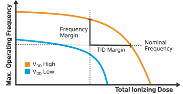
Diggins et al. presented [68] a timing window violation hypothesis (see Fig. 10) to explain the relationship between (i) TID degradation, (ii) operating frequency, and (iii) supply voltage. For each voltage, there is a maximum operating frequency at which software is executed successfully. This frequency decreases as the TID increases [21]. They proposed an external test to measure the impact of TID in the propagation delay of an ATMEGA328P microcontroller, observing violations on timing windows under multiple voltage and frequency conditions while the device was exposed to different values of TID and executed functional tests. Based on the observation that the operating core frequency controls the length of the timing windows, they ran software tests at different frequencies. For each value of TID, the maximum frequency at which the test passed was recorded. The authors reported that by overclocking the microcontroller above its nominal operational frequency, the degradation of the hardware was observable before a failure occurred at the nominal operating point. This last observation has the potential for monitoring techniques to activate predictive maintenance or graceful degradation approaches, such as operating at lower frequencies.
Discussion
The timing window violation hypothesis on microcontrollers has so far only been tested on TID-induced degradation, but we consider that its evaluation on other ageing mechanisms affecting signal propagation delay is still necessary. Although the analysis of timing window violation based on the clock frequency and operating voltage has mostly been tested in a laboratory, it presents great potential as an offline self-test due to the high clock configurability of many modern microcontrollers [81].
V-B SRAM Initial Pattern
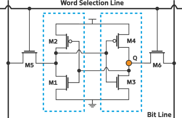
Many MCUs and FPGAs integrate static RAM (SRAM). A common implementation of an SRAM cell is the six-transistor circuit (see Fig. 11), owing to its relatively low static power usage. Each cell is composed of two cross-coupled inverters (M1, M2 and M3, M4) and two access transistors (M5 and M6). The cell has two stable states that represent either a logical 0 or 1, depending on the voltage at . The word selection line grants access to the cell and connects it to the bit line, which transfers data on read and write operations.
When a cell is energized, the initial value is not forced by the bit line; instead, it depends on the mismatch between the threshold voltage of the inverter transistors. The skew of an SRAM cell is its tendency towards a value when powered [82]. A non-skewed cell has a small threshold difference, and its initial value is random and depends on noise. These cells are commonly used as sources of entropy for random number generator systems. Cells with a moderate mismatch have a tendency towards a particular value, but this can be affected by ageing mechanisms. Finally, fully-skewed cells produce the same initial value with a high probability and can be used to implement SRAM physically unclonable functions.
The Static Noise Margin (SNM) of an SRAM cell is the minimum amount of voltage noise to flip its logic state. As the SNM depends on the transistor threshold voltage, ageing degrades it. Degraded SNM makes cells more sensitive to electric and thermal noise. A degradation of 15.02% of the SNM has been reported [83] after ten years of usage, owing to BTI effects. The skew of a cell is also impacted by BTI and HCI: Considering a cell that is constantly stressed by retaining a logical 1 on its output, P-MOS M2 transistor is active and undergoing a degradation process that modifies its threshold voltage during this time. If the gate threshold voltage of M2 is much larger than the one of M4, upon startup, the cell will be skewed towards 0 because M4 will be activated before M2.
The change in SRAM cells skew over time has been exploited by Guo et al. [66] as a two-phase method to detect recycled SoC and FPGA chips, later refined as a framework [67]. They proposed an initial enrolment phase to detect partially-skewed cells, which would likely change their startup value when aged. The authors first calculated the probability of starting in 0 and 1 for all SRAM bits, under room and high temperature, over a given number of startup cycles. The technique assumes that high ambient temperature produces a good prediction for the aged state of the bits. By calculating the difference between the probabilities and comparing it to a pre-selected gap value, they selected the “ageing-sensitive bits“. A chosen threshold value determined the number of flipped bits required to consider a device as used (i.e., aged) during the verification phase. It is noteworthy that the gap value used to select the ageing-sensitive bits is not universal, and the authors indicated that it should be determined based on measurements of aged devices beforehand. Tests on artificially-aged Xilinx Spartan-3 FPGAs showed false accept and reject rates of 0 and 0.03, respectively, when picking the proper parameters.
Guin et al. [65] also proposed a method to detect recycled SoCs and FPGAs based on the assumption that SRAM cells are balanced by design. The authors argued that any bias introduced during manufacture is random and that the amount of 1s and 0s normally distributes with a centre very close to 50% (i.e., within 1%). Therefore, any significant shift of the mean would be the result of circuit ageing. The technique requires no initial measurement phase nor a golden model against which to compare. The approach only requires that the circuit is powered-up multiple times to count the amount of 1s. The authors suggested having a large enough SRAM array (e.g., 64K bits) and taking enough successive measurements (e.g., 100) to minimize the impact of thermal noise during the assessment. Tests on COTS external SRAM chips showed significant changes in the values’ distribution (up to 14% after ageing) and a slight recovery when stress was removed.
Discussion
Given the ubiquity of SRAMs in all kinds of chips, using its initial pattern as an indicator of degradation is an interesting deployable method that requires no external equipment. Although related work shows that BTI effects are already detectable in a few hours of accelerated ageing, it remains to be studied whether the observable changes continue over time or the degradation saturates. Moreover, in order to utilize shifts in SRAM initial patterns as ageing monitoring, it is required to correlate their evolution with the degradation of parameters of interest, such as SNM.
V-C Electromagnetic (EM) Characteristics
Electronic device ageing affects EM characteristics such as conducted and radiated emissions [84] and susceptibility [70]. By subjecting devices to Electromagnetic Compatibility (EMC) tests, their effective ageing could be determined.
Dawson et al. [69] proposed a method to study the effect of high temperature ageing on the electromagnetic emissions of a COTS MCU. They argued that monitoring device emissions is a reliable and straightforward means to monitor ageing, as no electrical contact with the system is required. An emission test board was built, containing a Microchip PIC MCU whose pins were connected to loaded tracks passing by RF couplers. During the tests, the software running in the device toggled the pins while a spectrum analyser captured the emissions and the pins’ output voltage was measured. The authors reported variations in the emission spectra of artificially aged devices. Some harmonics of the central toggling frequency increased, particularly the high-frequency harmonics. It remains unclear whether a shift in the toggling frequency is the culprit. Additionally, the output voltage on aged devices increased. Finally, there were no conclusions regarding the reasons for the reported behaviour; thus, no clear mechanism linking the changes in emissions to device ageing was presented.
ElectroMagnetic Robustness (EMR) studies the impact of circuit ageing on EMC [85]. Li, Wu et al. [70, 86] studied the drift in the EM immunity of an MCU to Electrical Fast Transients (EFT) interference after accelerated ageing. They aged the device in incremental steps by applying high voltage (150% above nominal) and high temperature. The test setup consisted of a probe connecting the device to an EFT signal generator, which injected an interference signal between each ageing step. To assess whether the device was affected by the signal, errors in the executed software were monitored. The authors reported failures, including self-recovering errors, soft errors (reset was needed) and complete damage. Failure rates increased consistently with the ageing time, as well as immunity degradation (observed as a decrement in the maximum tolerated interference voltage for some pins). No deep analysis was made relating internal ageing mechanisms and the observed results. Instead, it was speculated that: (i) physical parameters of the functional components of the MCU drifted due to ageing, and (ii) components of the EM interference protection circuitry degraded, thus increasing susceptibility.
Discussion
Although related work reveals a clear impact of circuit degradation in the EMC and EMR of MCUs, the inner dynamics of this phenomenon are not fully clear. As MCUs are complex devices, it is no simple task to assess the degradation of every subsystem and their impact on the EM spectrum signature. EM measurements have not been widely developed as ageing monitoring techniques. This may owe to requiring external equipment and not fully grasping the correlation between system degradation (from the circuit operation point of view) and the changes in EM characteristics.
VI Ageing Detection on Power Supplies
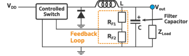
All embedded systems require supplies to deliver power with stable parameters over the entire lifespan of the application. Due to their high efficiency (typically more than 90%), Switching Mode Power Supplies (SMPS) are a popular choice to provide a stable DC voltage. SMPS are commonly composed of a switching transistor, a diode, a component that accumulates energy (usually an inductor) and a capacitor completing an LC filter for a steady DC output. Depending on their application, they can be built in a step-up (boost) configuration – reducing current and increasing voltage – or in a step-down (buck) configuration (see Fig. 12) – increasing the delivered current by decreasing the voltage. The controlled switch continuously switches between ON and OFF (at which ideally there is no power dissipation). The output voltage is regulated by controlling the switching signal’s duty cycle.
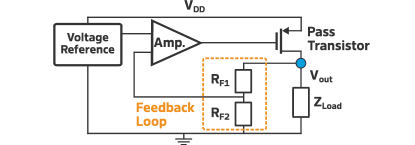
Low Drop-Out (LDO) linear voltage regulators (see Fig. 13) can regulate their output even when the input voltage (power supply) is close to the output voltage. They are commonly found as stand-alone chips in many power delivery networks of embedded systems and integrated into ICs and SoCs. An LDO is composed of an operational amplifier, a voltage reference, a pass transistor and a resistive divider which closes a feedback loop. The amplifier constantly compares the feedback loop voltage with the expected value of the reference. Based on this value, the amplifier controls the gate voltage of the transistor, which acts as a variable resistance and sets the feedback voltage (and thus the output voltage) to the desired value. Although simpler than SMPS, LDO’s drawback is lower efficiency. As the voltage regulation is performed by the pass transistor in its ohmic region, it actively dissipates energy.
The most popular choices for power supply in embedded applications are built with components that undergo ageing, as described in Section II. In this section, we present several techniques used to detect and monitor the degradation of power supply performances and shifts in their parameters.
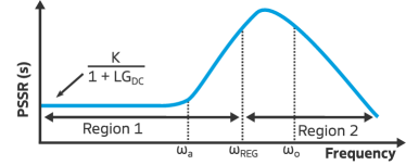
VI-A Power Supply Rejection Ratio
Power Supply Rejection Ratio (PSRR) is an important characteristic of LDO regulators. It indicates a regulator’s ability to prevent fluctuations in the output voltage when there is noise in the input voltage (or power supply voltage). PSRR is the relation between the output voltage ripple and the input voltage ripple and is normally measured for the whole operating frequency band of the regulator. A typical PSRR characteristic is illustrated in Fig. 14; a lower value means a better rejection of the power supply noise. PSRR in the frequency domain can be modelled as in Eq. 10 [71]. The constant depends on the feedback resistors, the load and the internal drain-to-source resistance to the small signal of the transistor. The frequencies and are poles of the PSRR transference equation and depend on the resistances and capacitances of the transistor, the amplifier, and the load circuit. and are the loop gains of the amplifier and pass transistor, respectively.
| (10) | ||||
| with the feedback loop transfer function, | ||||
| (11) | ||||
The PSSR curve has two regions: Region 1 at low and middle frequencies and Region 2 at high frequencies. Both regions meet at the unity bandwidth frequency , where the feedback loop gain is one. Region 1 is governed by the loop gain, which depends on the transconductance of the pass transistor and the amplifier. As this property is affected by transistor ageing mechanisms (e.g., BTI and HCI), PSRR is impacted by circuit ageing. Region 2 is mainly impacted by parasitic capacitances of the transistor input and the load, while the feedback loop gain plays almost no role. HCI changes the gate capacitance of transistors [87], thus modifying PSRR also in this region.
Considering the effect of circuit ageing on PSRR, Chowdhury et al. [77] proposed using this parameter to estimate the ageing of LDOs, as well as ICs, including such components in their power delivery networks, in order to determine whether a device has been recycled. To characterize the impact of ageing in PSRR, the authors designed their own LDO chips in 65 nm technology. The LDOs were artificially aged at elevated temperature and power supply voltage. To analyse the PSRR of the devices and to record the output spectrum, a spectrum analyser and its tracking generator were employed. After applying AC and DC stress to the LDO, a degradation of PSRR was observed, as well as a shift in the transfer poles.
Based on the clear influence of circuit ageing on PSRR [77], the authors introduced a technique [78, 71] based on machine learning methods that utilizes this parameter to detect recycled analog and mixed-signal chips and SoCs, respectively. As a first step, an unsupervised k-Nearest Neighbours (KNN) model was trained and tested with PSRR data from new and artificially aged devices from a single vendor. Next, the authors used a semi-supervised approach, where they used the previously-trained models (from a single vendor) and tested them against other vendors in an attempt to avoid requiring golden data from all vendors. Both approaches showed promising results in discriminating used and new LDOs, but required golden data and a supervised training phase. Finally, for unsupervised learning, two cases were tested: (i) PSRR data from an unknown device is given to the model together with golden data, and based on the number of clusters returned, the device can be classified as new or aged. (ii) The PSRR of the unknown device is measured twice, before and after a synthetic ageing process. This last approach has the clear downside of being partially destructive and has not shown good results.
Acharya et al. [72] presented and implemented an odometer based on a modified LDO circuit intended for the ageing-based detection of recycled ICs. A parallel feedback path to the regulator (i.e., a reference path) was added, which remained unused throughout the device’s lifetime. Two signals controlled which path is actively used. A one-label classifier model evaluated the LDO’s PSRR when using each path to detect degradation in the regulator’s components. Besides the external measurements, this method has the drawbacks of requiring a custom regulator design (i.e., cannot be applied on COTS components) and employing redundant hardware.
Discussion
Measuring PSRR changes has proved to be an effective method for detecting ageing of external LDO regulators. Although Chowdhury et al. claim that the proposed methods [77, 78] are to be used on ICs, they were only tested on stand-alone LDOs. Only in [71] measurements of embedded LDOs were presented, but the used models could not detect recycled chips. In addition, the reported results are based on artificially aged devices due to the lack of used chips. Given its direct relation to transistor parameters, PSRR is a sensible parameter to indicate the age of an LDO, but the literature thus far has only focused on short ageing periods (a few hours under accelerated ageing correspond to a few days of normal operation). To fully understand whether PSRR can correlate to device ageing over longer periods of time, further research in this direction is required. Moreover, methods proposed so far heavily rely on external testing equipment, and no strategy has been yet presented to deploy them on the field.
VI-B Electromagnetic Characteristics
Ageing affects not only the EM characteristics of microcontrollers and SoCs (Section V-C) but also of LDOs [79] and SMPSs [6]. Indeed, as parameters of the voltage regulator’s components shift from their nominal values due to degradation mechanisms, so do their EM emissions and susceptibility.
Boyer et al. [6] have studied how thermally-triggered ageing mechanisms affect internal components of SMPS in step-down or buck configuration, thus modifying its conducted and radiated EM emissions. To this end, they have artificially aged 4 samples of NCP3163 devices at elevated temperature. Although all samples were operational after ageing, an average increase between 6 and 20 dB in the conducted emissions and 5 dB in the radiated emissions spectra were observed over a large frequency range. The aged inductor was replaced by a new component to determine its impact on the system degradation. This lowered the EM emissions to the initial value. By means of an impedance vs. frequency characterization of the inductor before and after the thermal stress, the authors encountered a reduction in its impedance and quality factor, which was attributed to an increase in the parasitic parallel capacitor caused by a higher core loss.
Boyer et al. also performed similar experiments [76] on synchronous buck converters based on the LT3800 controller. Measurements of conducted EM emissions were carried out inside a semi-anechoic chamber. Converter boards and various additional components were aged in an oven at high temperature for two weeks. The power iron inductor and aluminium capacitor were the most degraded components, followed by the onboard output capacitor and the power transistors. In addition, the conducted emission measured at the circuit output suffered an increment of up to 15 dB between 4 and 100 MHz.
As analysed in detail by Wu et al. [79], a common failure mode caused by EM noise coupled to the power pin of an LDO is the EMI-induced offset. Due to the nonlinearity of the differential transistor pair at the input of the comparator amplifier (see Fig. 13), noise injected via the power network induces an offset of the output voltage via a rectification effect. A test bench was built, with a signal generator coupled to the voltage source and an oscilloscope monitoring the output and reference voltage. Various devices were aged for a week by electrically stressing them to evaluate the relation between ageing mechanisms and EM susceptibility. The devices still functioned, but their EMI robustness decreased. This indicated that the stress process had indeed triggered the transistor ageing mechanisms in the operational amplifier of the LDO.
Discussion
Component degradation negatively affects EM emissions and susceptibility power supplies. Although EM characteristics are indicators of the components’ ageing status, measuring them can be troublesome. Ageing detection methods in the literature based on EM measurements typically require special setups, procedures, and external equipment, hindering the ability to deploy them as monitoring techniques. Moreover, the usage of expensive dedicated instruments contradicts many typical constraints for COTS-based embedded applications, namely low cost, power usage, and size.
VI-C Capacitor’s Equivalent Series Resistance (ESR)
Capacitors are widely used as low-pass filters to clean noise from power lines (e.g., to suppress the switching noise introduced by SMPS, see Fig. 12). Capacitor degradation jeopardizes the availability of the circuit. In fact, electrolytic capacitor failures cause more than 50% of SMPS breakdowns [75]. As digital components require a stable voltage, capacitors are attractive for degradation studies.
The impact of ageing mechanisms on the output voltage ripple of SMPS has been studied in [6]. Several DC-DC switching step-down circuits were subjected to accelerated ageing via increased temperature. The authors reported an increase between 100% and 200% in the output noise after ageing. It was determined that the main culprits for the decay in the voltage stability were the filtering electrolytic capacitors at the output. Indeed, the high temperature accelerated the ageing mechanism described in Section II-C1. As a consequence, the equivalent serial resistance increased, and the capacitance decayed.
As the ESR usually changes more than the capacitance for a given ageing, the former is preferred for monitoring purposes. To prevent failures, it is usually a good practice to replace a component whose ESR has increased by 100% or more [31].
Givi et al. [73] have proposed and implemented an online monitoring system for DC-DC converters. Their technique detects ageing in the power supply output capacitor by indirectly measuring its ESR. The proposed setup required two voltage sensors: a Rogowski coil sensor on the converter’s inductor and a sensor of the output voltage. The authors implemented a monitoring system that derived the capacitor’s ESR on software from measurements of these two voltages using a DS1104 controller board. By comparing the resistance value with the initial one, the degradation of the component was estimated, and a warning signal could be triggered.
Lahyani et al. argued [75] that the only waveform that changes when capacitors degrade is the output voltage ripple. They developed a software-based ESR monitoring method that sampled this ripple and applied a band-pass filter to the signal. They stated that measuring the ripple at the power supply switching frequency is a more realistic method than using an average rectified value, and it reduces the load dependence.
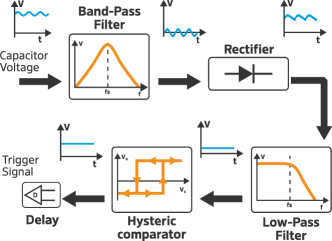
On the other hand, Chen et al. [74] also measured ESR by observing the output voltage but proposed to filter the switching frequency out. After theoretical analysis, the authors concluded that the amplitude of the output voltage ripple could be accurately modelled directly as linearly dependent on the ESR. Additionally, they showed that, as the capacitor is part of an LC filter, the output voltage ripple has almost no variation due to changes in the load current. This allowed them to propose a failure prediction method which measured and processed the capacitor voltage, illustrated in Fig. 15. A band-pass filter eliminated the DC component and the power supply switching frequency from the signal. After injecting the signal into a rectifier and a low-pass filter, a voltage proportional to the capacitor ESR was obtained. When compared with a pre-defined threshold voltage, an early warning trigger signal was obtained. An additional delay circuit served to mitigate fake measurements during the circuit startup transient.
Discussion
Literature shows that the output capacitor ESR is a good indicator to assess the overall health of a power supply. On the one hand, this measurement is relatively simple. Given the ubiquity of analog-to-digital converters in most modern microcontrollers found in embedded applications, it would be of interest to develop a built-in online test that performed the signal processing completely digitally and required no extra circuitry. On the other hand, a drawback of this approach is the high susceptibility of ESR to operating conditions. Although it has been shown [73, 75, 74] that changes in the load do not affect the measurement, ESR still changes significantly with temperature and frequency. Systems need to additionally measure the environment and keep a record of the initial value under different conditions to account for these changes.
VII Conclusion and Outlook
In this survey, we reviewed and systematized methods and solutions for detecting hardware ageing on FPGAs, SoCs, microcontrollers, and on their power supplies. This work was motivated by the increasing deployment of such embedded systems in varying contexts of criticality as well as in harsh operational environments. Many deployment locations are, in addition, hard to access, either because they are widely distributed in the IoT or because the environmental conditions prevent accessibility (e.g., particle accelerators’ tunnels with high radiation). Systems should be autonomous in these situations, not only for normal operations but also in their ability to monitor and diagnose themselves.
The existing body of literature showed extensive research towards the implementation and deployment of self-tests for FPGAs. Indeed, their re-programmable nature makes them excellent candidates for synthesizing test resources which can later be removed during operation. Nevertheless, techniques to assess or monitor degradation on microcontrollers, SoCs, and power supplies have focused on external tests, mainly to understand the impact of ageing processes. In this sense, BIST and SBST for physical degradation effects on these components require further investigation.
With this overview, we want to foster future research and development towards self-aware embedded systems which not only can detect the degradation of individual hardware components but are able to assess their overall health status and predict a remaining lifetime. A corresponding research program could be guided along the following questions.
-
1.
Is it possible to reuse the working principles of external tests on SoCs, microcontrollers, etc. to derive in-situ self-tests of physical device degradation?
-
2.
Can we identify lightweight, easily measurable indicators that represent the overall health of the system well?
-
3.
Can we derive reliable system functions for health monitoring and self-assessment from these early indicators?
-
4.
Is there a versatile lifetime model that allows for predicting system failures based on the indicators available from the self-assessment?
Acknowledgement
We acknowledge the support by DASHH (Data Science in Hamburg - HELMHOLTZ Graduate School for the Structure of Matter) with the Grant-No. HIDSS-0002.
References
- [1] S. Khan, S. Hamdioui, H. Kukner, P. Raghavan, and F. Catthoor, “BTI impact on logical gates in nano-scale CMOS technology,” in 2012 IEEE 15th International Symposium on Design and Diagnostics of Electronic Circuits & Systems (DDECS), 2012, pp. 348–353.
- [2] E. Baccelli et al., “RIOT: an Open Source Operating System for Low-end Embedded Devices in the IoT,” IEEE Internet of Things Journal, vol. 5, no. 6, pp. 4428–4440, December 2018.
- [3] D. J. Smith, “2 - understanding terms and jargon,” in Reliability, Maintainability and Risk (Seventh Edition), seventh edition ed., D. J. Smith, Ed. Oxford: Butterworth-Heinemann, 2005, pp. 11–23.
- [4] E. Stott, J. S. Wong, and P. Y. Cheung, “Degradation analysis and mitigation in FPGAs,” in 2010 International Conference on Field Programmable Logic and Applications, 2010, pp. 428–433.
- [5] M. Gasperi, “Life prediction model for aluminum electrolytic capacitors,” in IAS ’96. Conference Record of the 1996 IEEE Industry Applications Conference Thirty-First IAS Annual Meeting, vol. 3, 1996, pp. 1347–1351 vol.3.
- [6] A. Boyer, H. Huang, and S. Ben Dhia, “Impact of thermal aging on emission of a buck dc-dc converter,” in 2014 International Symposium on Electromagnetic Compatibility, Tokyo, 2014, pp. 77–80.
- [7] D. K. Schroder, “Negative bias temperature instability: What do we understand?” Microelectronics Reliability, vol. 47, no. 6, pp. 841–852, 2007, modelling the Negative Bias Temperature Instability.
- [8] T. Grasser et al., “The paradigm shift in understanding the bias temperature instability: From reaction-diffusion to switching oxide traps,” IEEE Transactions on Electron Devices, vol. 58, no. 11, pp. 3652–3666, 2011.
- [9] J. Stathis, M. Wang, and K. Zhao, “Reliability of advanced high-k/metal-gate n-FET devices,” Microelectronics Reliability, vol. 50, no. 9, pp. 1199–1202, 2010, 21st European Symposium on the Reliability of Electron Devices, Failure Physics and Analysis.
- [10] K. O. Jeppson and C. M. Svensson, “Negative bias stress of MOS devices at high electric fields and degradation of MNOS devices,” Journal of Applied Physics, vol. 48, no. 5, pp. 2004–2014, 1977.
- [11] S. Ogawa and N. Shiono, “Generalized diffusion-reaction model for the low-field charge-buildup instability at the si- interface,” Phys. Rev. B, vol. 51, pp. 4218–4230, Feb 1995.
- [12] S. Rangan, N. Mielke, and E. Yeh, “Universal recovery behavior of negative bias temperature instability [pmosfets],” in IEEE International Electron Devices Meeting 2003, 2003, pp. 14.3.1–14.3.4.
- [13] M. Ershov et al., “Dynamic recovery of negative bias temperature instability in p-type metal-oxide-semiconductor field-effect transistors,” Applied Physics Letters, vol. 83, no. 8, pp. 1647–1649, 2003.
- [14] J. Stathis and S. Zafar, “The negative bias temperature instability in MOS devices: A review,” Microelectronics Reliability, vol. 46, no. 2, pp. 270–286, 2006.
- [15] A. Strong et al., Hot Carriers. John Wiley & Sons, Ltd, 2009, ch. 5, pp. 441–516.
- [16] C. Hu, S. C. Tam, F.-C. Hsu, P.-K. Ko, T.-Y. Chan, and K. Terrill, “Hot-electron-induced MOSFET degradation - model, monitor, and improvement,” IEEE Journal of Solid-State Circuits, vol. 20, no. 1, pp. 295–305, 1985.
- [17] T. H. Ning, P. W. Cook, R. H. Dennard, C. M. Osburn, S. E. Schuster, and H. N. Yu, “1-micron MOSFET VLSI technology. IV - Hot-electron design constraints,” IEEE Journal of Solid-State Circuits, vol. 14, pp. 268–275, Apr. 1979.
- [18] E. Takeda and N. Suzuki, “An empirical model for device degradation due to hot-carrier injection,” IEEE Electron Device Letters, vol. 4, no. 4, pp. 111–113, 1983.
- [19] T. Nigam, K. Y. Yiang, and A. Marathe, “Moore’s law: Technology scaling and reliability challenges,” 2017.
- [20] H. J. Barnaby, “Total-ionizing-dose effects in modern CMOS technologies,” IEEE Transactions on Nuclear Science, vol. 53, no. 6, pp. 3103–3121, 2006.
- [21] G. J. Schlenvogt, H. J. Barnaby, J. Wilkinson, S. Morrison, and L. Tyler, “Simulation of TID effects in a high voltage ring oscillator,” IEEE Transactions on Nuclear Science, vol. 60, no. 6, pp. 4547–4554, 2013.
- [22] M. Nancekievill, S. Watson, P. R. Green, and B. Lennox, “Radiation tolerance of commercial-off-the-shelf components deployed in an underground nuclear decommissioning embedded system,” in 2016 IEEE Radiation Effects Data Workshop (REDW), 2016, pp. 1–5.
- [23] R. Kingsbury et al., “TID tolerance of popular cubesat components,” in 2013 IEEE Radiation Effects Data Workshop (REDW), 2013, pp. 1–4.
- [24] C. Sharma, P. Rajesh, R. Behera, and S. Amirthapandian, “Impact of gamma radiation on 8051 microcontroller performance,” Nuclear Engineering and Technology, 2022.
- [25] T. Fried et al., “Radiation testing of low cost, commercial off the shelf microcontroller board,” Nuclear Engineering and Technology, vol. 53, no. 10, pp. 3335–3343, 2021.
- [26] T. R. Oldham, “Analysis of damage in MOS devices for several radiation environments,” IEEE Transactions on Nuclear Science, vol. 31, no. 6, pp. 1236–1241, 1984.
- [27] M. Shaneyfelt, J. Schwank, D. Fleetwood, P. Winokur, K. Hughes, and F. Sexton, “Field dependence of interface-trap buildup in polysilicon and metal gate MOS devices,” IEEE Transactions on Nuclear Science, vol. 37, no. 6, pp. 1632–1640, 1990.
- [28] G. Moore, “Cramming more components onto integrated circuits,” Proceedings of the IEEE, vol. 86, no. 1, pp. 82–85, 1998.
- [29] C. V. Thompson and J. R. Lloyd, “Electromigration and ic interconnects,” MRS Bulletin, vol. 18, no. 12, pp. 19–25, Dec 1993.
- [30] J. Black, “Electromigration–a brief survey and some recent results,” IEEE Transactions on Electron Devices, vol. 16, no. 4, pp. 338–347, 1969.
- [31] M. Gasperi, “A method for predicting the expected life of bus capacitors,” in IAS ’97. Conference Record of the 1997 IEEE Industry Applications Conference Thirty-Second IAS Annual Meeting, vol. 2, 1997, pp. 1042–1047 vol.2.
- [32] M. A. Kochte and H.-J. Wunderlich, “Self-test and diagnosis for self-aware systems,” IEEE Design & Test, vol. 35, no. 5, pp. 7–18, 2018.
- [33] IEEE, “Ieee standard framework for prognostics and health management of electronic systems,” IEEE Std 1856-2017, pp. 1–31, 2017.
- [34] G. Martino, A. Gruenhagen, J. Branlard, A. Eichler, G. Fey, and H. Schlarb, “Comparative evaluation of semi-supervised anomaly detection algorithms on high-integrity digital systems,” in 2021 24th Euromicro Conference on Digital System Design (DSD), 2021, pp. 123–130.
- [35] V. Agrawal, C. Kime, and K. Saluja, “A tutorial on built-in self-test. i. principles,” IEEE Design & Test of Computers, vol. 10, no. 1, pp. 73–82, 1993.
- [36] E. J. McCluskey, “Built-in self-test techniques,” IEEE Design & Test of Computers, vol. 2, no. 2, pp. 21–28, 1985.
- [37] A. Krstic, W.-C. Lai, K.-T. Cheng, L. Chen, and S. Dey, “Embedded software-based self-test for programmable core-based designs,” IEEE Design & Test of Computers, vol. 19, no. 4, pp. 18–27, 2002.
- [38] N. Kranitis, A. Paschalis, D. Gizopoulos, and G. Xenoulis, “Software-based self-testing of embedded processors,” IEEE Transactions on Computers, vol. 54, no. 4, pp. 461–475, 2005.
- [39] Z. Czaja, “Using a square-wave signal for fault diagnosis of analog parts of mixed-signal electronic embedded systems,” IEEE Transactions on Instrumentation and Measurement, vol. 57, no. 8, pp. 1589–1595, 2008.
- [40] K. M. Zick and J. P. Hayes, “On-line sensing for healthier FPGA systems,” in Proceedings of the 18th Annual ACM/SIGDA International Symposium on Field Programmable Gate Arrays, ser. FPGA ’10. New York, NY, USA: ACM, 2010, pp. 239–248.
- [41] P. Pfeifer, B. Kaczer, and Z. Pliva, “A reliability lab-on-chip using programmable arrays,” in 2014 IEEE International Reliability Physics Symposium, 2014, pp. CA.6.1–CA.6.8.
- [42] P. Pfeifer and Z. Pliva, “On measurement of parameters of programmable microelectronic nanostructures under accelerating extreme conditions (xilinx 28nm xc7z020 zynq fpga),” in 2013 23rd International Conference on Field programmable Logic and Applications, 2013, pp. 1–4.
- [43] P. Pfeifer and Z. Pliva, “On measurement of impact of the metallization and fpga design to the changes of slice parameters and generation of delay faults,” in 22nd International Conference on Field Programmable Logic and Applications (FPL), 2012, pp. 743–746.
- [44] P. Sedcole and P. Y. K. Cheung, “Within-die delay variability in 90nm FPGAs and beyond,” in 2006 IEEE International Conference on Field Programmable Technology, 2006, pp. 97–104.
- [45] K. Maragos, E. Taka, G. Lentaris, I. Stratakos, and D. Soudris, “Analysis of performance variation in 16nm FinFET FPGA devices,” in 2019 29th International Conference on Field Programmable Logic and Applications (FPL), 2019, pp. 38–44.
- [46] F. Bruguier, P. Benoit, P. Maurine, and L. Torres, “A new process characterization method for FPGAs based on electromagnetic analysis,” in 2011 21st International Conference on Field Programmable Logic and Applications, 2011, pp. 20–23.
- [47] M. Naouss and F. Marc, “Design and implementation of a low cost test bench to assess the reliability of fpga,” Microelectronics Reliability, vol. 55, no. 9, pp. 1341–1345, 2015, proceedings of the 26th European Symposium on Reliability of Electron Devices, Failure Physics and Analysis.
- [48] M. Naouss and F. Marc, “Modelling delay degradation due to NBTI in FPGA look-up tables,” in 2016 26th International Conference on Field Programmable Logic and Applications (FPL), 2016, pp. 1–4.
- [49] M. Naouss and F. Marc, “FPGA LUT delay degradation due to HCI: Experiment and simulation results,” Microelectronics Reliability, vol. 64, pp. 31–35, 2016, proceedings of the 27th European Symposium on Reliability of Electron Devices, Failure Physics and Analysis.
- [50] F. Ahmed, M. Shintani, and M. Inoue, “Accurate recycled fpga detection using an exhaustive-fingerprinting technique assisted by WID process variation modeling,” IEEE Transactions on Computer-Aided Design of Integrated Circuits and Systems, vol. 40, no. 8, pp. 1626–1639, 2021.
- [51] M. Ruffoni and A. Bogliolo, “Direct measures of path delays on commercial FPGA chips,” in Proceedings: 6th IEEE Workshop on Signal Propagation on Interconnects, 2002, pp. 157–159.
- [52] A. Amouri, F. Bruguier, S. Kiamehr, P. Benoit, L. Torres, and M. Tahoori, “Aging effects in FPGAs: an experimental analysis,” in 2014 24th International Conference on Field Programmable Logic and Applications (FPL), 2014, pp. 1–4.
- [53] C. Leong et al., “Aging monitoring with local sensors in FPGA-based designs,” in 2013 23rd International Conference on Field programmable Logic and Applications, 2013, pp. 1–4.
- [54] M. D. Valdes-Peña et al., “Design and validation of configurable online aging sensors in nanometer-scale FPGAs,” IEEE Transactions on Nanotechnology, vol. 12, no. 4, pp. 508–517, 2013.
- [55] M. Valdés et al., “Programmable sensor for on-line checking of signal integrity in FPGA-based systems subject to aging effects,” in 2011 12th Latin American Test Workshop (LATW), 2011, pp. 1–7.
- [56] J. Li and J. Lach, “Negative-skewed shadow registers for at-speed delay variation characterization,” in 2007 25th International Conference on Computer Design, 2007, pp. 354–359.
- [57] A. Amouri and M. Tahoori, “A low-cost sensor for aging and late transitions detection in modern FPGAs,” in 2011 21st International Conference on Field Programmable Logic and Applications, 2011, pp. 329–335.
- [58] Z. Ghaderi, M. Ebrahimi, Z. Navabi, E. Bozorgzadeh, and N. Bagherzadeh, “SENSIBle: A highly scalable sensor design for path-based age monitoring in FPGAs,” IEEE Transactions on Computers, vol. 66, no. 5, pp. 919–926, 2017.
- [59] P. Pfeifer and Z. Pliva, “Delay-fault run-time XOR-less aging detection unit using BRAM in modern FPGAs,” in 2012 13th Biennial Baltic Electronics Conference, 2012, pp. 81–84.
- [60] W. Jiang, R. Li, H. Yu, and Y. Ha, “An accurate FPGA online delay monitor supporting all timing paths,” in 2020 IEEE International Symposium on Circuits and Systems (ISCAS), 2020, pp. 1–5.
- [61] J. S. J. Wong, P. Sedcole, and P. Y. K. Cheung, “Self-characterization of combinatorial circuit delays in FPGAs,” in 2007 International Conference on Field-Programmable Technology, 2007, pp. 17–23.
- [62] J. S. J. Wong, P. Sedcole, and P. Y. K. Cheung, “Self-measurement of combinatorial circuit delays in fpgas,” ACM Trans. Reconfigurable Technol. Syst., vol. 2, no. 2, jun 2009.
- [63] E. A. Stott, J. S. Wong, P. Sedcole, and P. Y. Cheung, “Degradation in FPGAs: Measurement and modelling,” in Proceedings of the 18th Annual ACM/SIGDA International Symposium on Field Programmable Gate Arrays, ser. FPGA ’10. New York, NY, USA: ACM, 2010, pp. 229–238.
- [64] J. S. J. Wong, P. Sedcole, and P. Y. K. Cheung, “A transition probability based delay measurement method for arbitrary circuits on fpgas,” in 2008 International Conference on Field-Programmable Technology, 2008, pp. 105–112.
- [65] U. Guin, W. Wang, C. Harper, and A. D. Singh, “Detecting recycled SoCs by exploiting aging induced biases in memory cells,” in 2019 IEEE International Symposium on Hardware Oriented Security and Trust (HOST), 2019, pp. 72–80.
- [66] Z. Guo, M. T. Rahman, M. M. Tehranipoor, and D. Forte, “A zero-cost approach to detect recycled SoC chips using embedded SRAM,” in 2016 IEEE International Symposium on Hardware Oriented Security and Trust (HOST), 2016, pp. 191–196.
- [67] Z. Guo, X. Xu, M. T. Rahman, M. M. Tehranipoor, and D. Forte, “SCARe: An SRAM-based countermeasure against IC recycling,” IEEE Transactions on Very Large Scale Integration (VLSI) Systems, vol. 26, no. 4, pp. 744–755, 2018.
- [68] Z. J. Diggins et al., “Total-ionizing-dose induced timing window violations in CMOS microcontrollers,” IEEE Transactions on Nuclear Science, vol. 61, no. 6, pp. 2979–2984, 2014.
- [69] J. F. Dawson, I. D. Flintoft, A. P. Duffy, A. C. Marvin, and M. P. Robinson, “Effect of high temperature ageing on electromagnetic emissions from a PIC microcontroller,” in 2014 International Symposium on Electromagnetic Compatibility, 2014, pp. 1139–1143.
- [70] C. Li, J. Wu, Y. Huang, and W. Zhu, “Characterization of change in microcontroller susceptibility during accelerated aging,” in 2016 Asia-Pacific International Symposium on Electromagnetic Compatibility (APEMC), vol. 01, 2016, pp. 751–754.
- [71] S. Chowdhury, F. Ganji, and D. Forte, “Recycled SoC detection using LDO degradation,” SN Computer Science, vol. 1, no. 6, p. 312, Sep 2020.
- [72] R. Y. Acharya, M. Valentin Levin, and D. Forte, “LDO-based odometer to combat ic recycling,” in 2021 IEEE 34th International System-on-Chip Conference (SOCC), 2021, pp. 206–211.
- [73] H. Givi, E. Farjah, and T. Ghanbari, “A comprehensive monitoring system for online fault diagnosis and aging detection of non-isolated DC-DC converters’ components,” IEEE Transactions on Power Electronics, vol. 34, no. 7, pp. 6858–6875, 2019.
- [74] Y.-M. Chen, M.-W. Chou, and H.-C. Wu, “Electrolytic capacitor failure prediction of LC filter for switching-mode power converters,” in Fourtieth IAS Annual Meeting. Conference Record of the 2005 Industry Applications Conference, 2005., vol. 2, 2005, pp. 1464–1469 Vol. 2.
- [75] A. Lahyani, P. Venet, G. Grellet, and P.-J. Viverge, “Failure prediction of electrolytic capacitors during operation of a switchmode power supply,” IEEE Transactions on Power Electronics, vol. 13, no. 6, pp. 1199–1207, 1998.
- [76] A. Boyer, M. Gonzalez Sentis, C. Ghfiri, and A. Durier, “Study of the thermal aging effect on the conducted emission of a synchronous buck converter,” in 2017 11th International Workshop on the Electromagnetic Compatibility of Integrated Circuits (EMCCompo), 2017, pp. 79–84.
- [77] S. Chowdhury, H. Shen, B. Park, N. Maghari, and D. Forte, “Aging analysis of low dropout regulator for universal recycled ic detection,” in 2019 IEEE Computer Society Annual Symposium on VLSI (ISVLSI), 2019, pp. 604–609.
- [78] S. Chowdhury, F. Ganji, T. Bryant, N. Maghari, and D. Forte, “Recycled analog and mixed signal chip detection at zero cost using LDO degradation,” in 2019 IEEE International Test Conference (ITC), 2019, pp. 1–10.
- [79] J. Wu, J. Li, R. Shen, A. Boyer, and S. Ben Dhia, “Effect of electrical stresses on the susceptibility of a voltage regulator,” in 2013 International Symposium on Electromagnetic Compatibility, 2013, pp. 759–764.
- [80] A. Ghosh, S. Devadas, K. Keutzer, and J. White, “Estimation of average switching activity in combinational and sequential circuits,” in [1992] Proceedings 29th ACM/IEEE Design Automation Conference, 1992, pp. 253–259.
- [81] M. Rottleuthner, T. C. Schmidt, and M. Wählisch, “Dynamic Clock Reconfiguration for the Constrained IoT and its Application to Energy-efficient Networking,” in International Conference on Embedded Wireless Systems and Networks (EWSN’22). New York, USA: ACM, October 2022.
- [82] D. E. Holcomb, W. P. Burleson, and K. Fu, “Power-up SRAM state as an identifying fingerprint and source of true random numbers,” IEEE Transactions on Computers, vol. 58, no. 9, pp. 1198–1210, 2009.
- [83] R. Faraji and H. R. Naji, “Adaptive technique for overcoming performance degradation due to aging on 6t SRAM cells,” IEEE Transactions on Device and Materials Reliability, vol. 14, no. 4, pp. 1031–1040, 2014.
- [84] A. Boyer, S. B. Dhia, B. Li, N. Berbel, and R. Fernandez-Garcia, “Experimental investigations into the effects of electrical stress on electromagnetic emission from integrated circuits,” IEEE Transactions on Electromagnetic Compatibility, vol. 56, no. 1, pp. 44–50, 2014.
- [85] S. Ben Dhia, A. Boyer, l. Binhong, and A. Ndoye, “Characterisation of electromagnetic compatibility drifts of nanoscale integrated circuit after accelerated life tests,” Electronics Letters, vol. 46, pp. 278 – 280, 03 2010.
- [86] J. Wu, C. Li, B. Li, W. Zhu, and H. Wang, “Microcontroller susceptibility variations to EFT burst during accelerated aging,” Microelectronics Reliability, vol. 64, pp. 210–214, 2016, proceedings of the 27th European Symposium on Reliability of Electron Devices, Failure Physics and Analysis.
- [87] Y. Huh, Y. Sung, and S. Kang, “A study of hot-carrier-induced mismatch drift: a reliability issue for VLSI circuits,” IEEE Journal of Solid-State Circuits, vol. 33, no. 6, pp. 921–927, 1998.