Memory and transduction prospects for silicon centre devices
Abstract
The centre, a silicon-native spin-photon interface with telecommunications-band optical transitions and long-lived microwave qubits, offers an appealing new platform for both optical quantum memory and microwave to optical telecommunications band transduction. A wide range of quantum memory and transduction schemes could be implemented on such a platform, with advantages and disadvantages that depend sensitively on the ensemble properties. In this work we characterize centre spin ensembles to inform device design. We perform the first ensemble optical depth measurement and calculate the improvement in centre density or resonant optical enhancement required for efficient optical quantum memory. We further demonstrate a coherent microwave interface by coherent population trapping (CPT) and Autler-Townes splitting (ATS). We then determine the most promising microwave and optical quantum memory protocol for such ensembles. By estimating the memory efficiency both in free-space and in the presence of a cavity, we show that efficient optical memory is possible with forecast densities. Finally, we formulate a transduction proposal and discuss the achievable efficiency and fidelity.
I Introduction
Quantum memories and transducers are enabling technologies for the global quantum internet. Optical quantum memories that coherently store and recall unknown states of a traveling optical field on demand [1] are a component of quantum repeaters [2, 3, 4, 5] to enhance the entanglement distribution range, and therefore the secure communication range, of quantum networks [6] as well as a means of synchronizing processes with optical quantum computers. Microwave quantum memories, on the other hand, can interface with microwave frequency material qubits, including superconducting circuit qubits—arguably the most advanced quantum computing platform at present—to extend circuit depth and reduce no-op error rates [7].
Long-coherence spin ensembles have been proposed as quantum memories for both applications, with considerable research into optical quantum memories in particular. To date, several quantum memory protocols including electromagnetically induced transparency (EIT) [8], atomic frequency comb (AFC) [9], controlled reversible inhomogeneous broadening (CRIB) [10], and Autler-Townes Splitting (ATS) [11] have been proposed based on platforms such as rare-earth ions [12, 13], NV centres in diamond [14], atomic vapours [15, 16], and Bose-Einstein condensates (BEC) [17, 18]. However, few of these systems operate in a telecommunications (telecom) band. Extending the quantum internet to global scale requires optical quantum memories compatible with satellite communications as well as terrestrial optical fibre networks.
Similarly, efficient and coherent conversion between gigahertz microwave and terahertz optical signals is essential for networking microwave material qubits [19]. Transduction from microwave to telecom photons could enable, for example, networking superconducting quantum processors and spin quantum processors [20, 21] via the global quantum internet. There are several remarkable experimental demonstrations [22, 23, 24, 25] as well as theoretical approaches [26, 27, 28] on reversibly converting between microwave and optical fields. In general, quantum transduction can be carried out through intermediate systems such as atomic ensembles [26, 29, 22, 25], electro-optical systems [30, 24], electro-optomechanical [31, 23], and others [32, 33].
Ensembles of atoms or atom-like systems combining long-coherence microwave spin qubits and optical transitions are therefore a versatile ‘swiss-army knife’ platform suitable for microwave and optical memory as well as microwave to optical transduction. Identifying and developing long-coherence quantum systems combining narrow and absorptive microwave and telecom optical transitions is an important milestone for designing a quantum network. However, to date few suitable systems have been identified. Memory and transduction proposals of this kind have focused almost exclusively on Er3+, which combines narrow MW and telecom optical transitions in many crystal hosts [34, 26, 29]. Although the optical transition is comparatively weak, significant optical depths have been observed with concentrated Er3+ ensembles in large crystals [35].
The newly rediscovered silicon centre offers native O-band telecom access and long-lived spins operating at microwave frequencies [36, 37]. Notably, silicon is an attractive host material for such a system, as it is already the substrate of choice for a wide variety of quantum platforms including ion traps [38], quantum dots [39], superconducting qubits [40], and, naturally, impurity and defect spins in silicon [41] and silicon photonics [42]. The centre integrates with silicon photonic devices on CMOS-compatible wafers as a waveguide and fibre-networked quantum information platform [37] that could further mediate between other silicon quantum technologies packaged on-chip, such as superconducting, trapped ion and gate-defined quantum dot qubits, for a complete, all-silicon hybrid quantum information platform.
In this paper we introduce the prospects of centres for microwave quantum memory, optical quantum memory, and microwave-optical quantum transducers. We will first briefly review the known properties of the centre as revealed by recent studies. Then, we further characterize centre ensembles experimentally towards the goal of quantum memories and transducers. We measure centre optical depth (OD) in Section III, microwave coherent population trapping (CPT) in Section IV, and microwave Autler-Townes splitting in Section V. Informed by these measurements, in Section VI, we estimate the efficiency of applicable optical memory schemes including EIT and ATS. In Section VII we derive the resonator requirements for efficient centre microwave quantum memories. In Section VIII, we consider the potential of combining these ATS schemes to design a transduction protocol. Finally, we conclude with future directions in Section IX.
II The centre
The centre is a luminescent silicon defect with a sharp emission line at meV, in the telecommunications O band. Early work [43, 44] established that centres comprise two nonequivalent carbon atoms and a hydrogen atom. Some of the centre parameters required to calculate quantum memory and transduction efficiencies, including the level structure, optical linewidths and lifetimes, and spin coherence times have recently been established [36, 45, 37]. The remaining key parameters—optical depth, microwave coupling strengths and two-photon microwave linewidth—are obtained in this work and put to use in proof-of-principle quantum memory precursor experiments.
Spectroscopy of centre ensembles [36] established that the ground state has a tightly bound s = 1/2 electron coupled to the hydrogen nuclear s = 1/2 spin through an anisotropic hyperfine interaction. In its optically excited state a bound exciton is formed, the electron spins form a singlet state, and there remains an unpaired s = 3/2 hole. The four-fold degeneracy of free holes in silicon is lifted in the reduced symmetry of the centre to form two distinct excited state doublets labeled TX0 and TX1 separated by meV. Thermal excitation between these two states is negligible below K. Studies of TX0 with ensembles and single centres revealed remarkable optical linewidths sufficient to resolve the ground state electron spin splitting at low fields [36, 37].
The TX0 lifetime is 0.94 s in bulk silicon [36]. The radiative efficiency, , of this transition is not precisely known. To date, measurements with bulk ensembles have not found evidence of non-radiative relaxation [36]. First-principles theoretical calculations indicate [46] and single-centre photon fluorescence rates bound [37]. The zero-phonon fraction, or Debye-Waller (DW) factor, is known to be [36].
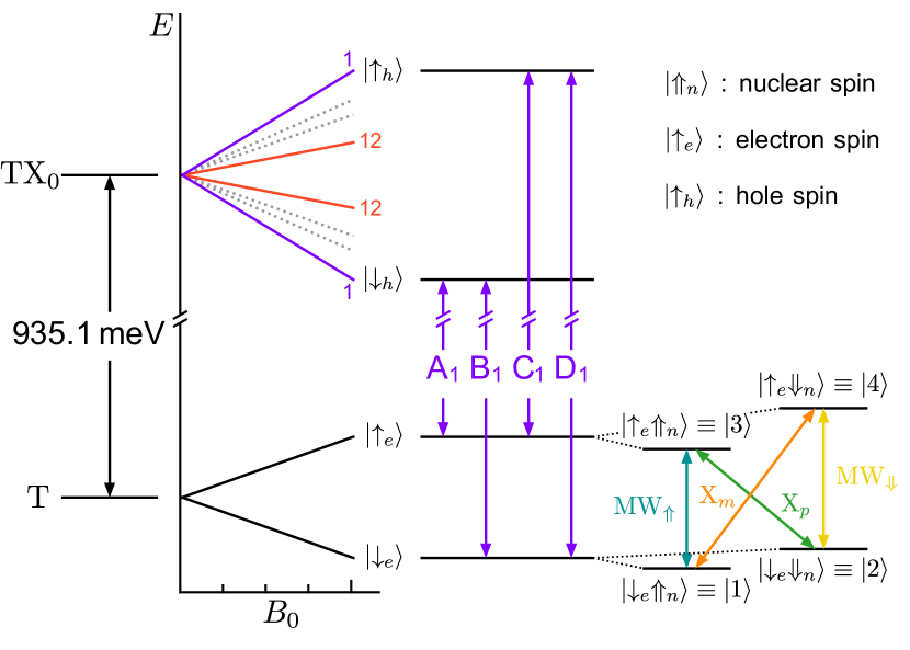
The schematic level structure in Fig. 1 shows TX0 under an applied magnetic field, with four resolved optical transitions A–D between the ground state electron and excited state hole states. The centre has 24 possible orientations forming 12 inequivalent inversion symmetric subsets , each with its own set of optical transitions Ai–Di determined by the effective anisotropic hole Landé factor for a particular magnetic field orientation. Optically detected magnetic resonances (ODMR) reveal ground state hyperfine splitting under microwave or RF excitation. Both the ‘allowed’ nuclear spin preserving microwave transitions, MW⇑ and MW⇓, and the ‘forbidden’ microwave transitions, Xm and Xp, are observed to be strong. The centre therefore boasts both optical and microwave and V transitions for interfacing between travelling fields and spins. The nuclear spin states of the hydrogen nucleus, which have not yet been optically resolved, would become optically accessible in lifetime-limited homogeneous ensembles.
Isotopically purified improves upon both the spin and optical properties of the centre. Removing 29Si atoms (spin 1/2 nuclei) reduces the magnetic noise bath and improves native spin coherence times. Removing mass variations due to both 29Si and 30Si dramatically reduces the optical inhomogeneous broadening. Ensemble optical inhomogeneous linewidths as low as MHz have been observed in centre ensembles [36]. Measurements of spectral diffusion have indicated that the ensemble optical linewidths may be close to diffusion limited, and that spectral diffusion remains low in natural silicon samples even as the inhomogeneous linewidth increases to GHz [45]. Hahn echo measurements in crystals revealed centre electron and nuclear spin coherence times () of ms and s respectively [36]. Both centre spins offer a memory advantage compared to superconducting qubits, and the nuclear spin coherence time is furthermore sufficient for repeaters in terrestrial quantum networks.
In the following sections we extend these studies by characterizing the optical absorption properties of centre ensembles to determine the requirements for centre optical quantum memories. We further implement the first coherent and V schemes for centres as a precursor to quantum memory and transduction protocols.
III Optical depth
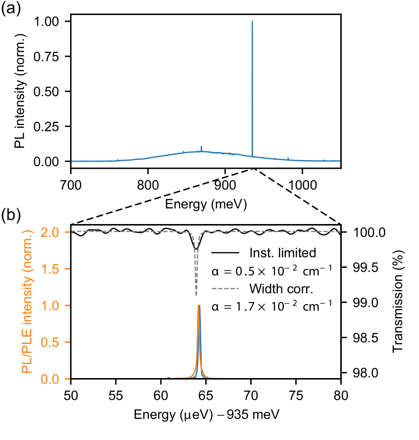
An efficient quantum memory fundamentally requires signal absorption approaching 100% for the reversible transfer of information. Here we report the first optical absorption measurements of centres and extrapolate what optical depths are feasible within the near term for centre quantum memories. An mm thick sample was electron-irradiated and annealed according to the procedure in APPENDIX B: METHODS to produce a significant concentration of centres. We measure the complete photoluminescence (PL) spectrum under above-band excitation with Fourier transform infrared (FTIR) spectroscopy, Fig. 2(a). Detail about the prominent TX0 ZPL is shown in Figure 2(b). In addition to the PL spectrum (blue), we resolve the ZPL by photoluminescence excitation (PLE) spectroscopy, resonantly exciting the TX0 with a scanning laser and detecting fluorescence from the centre phonon sideband to determine an ensemble ZPL linewidth of MHz (orange). This linewidth is an inhomogeneous factor of 331 over the lifetime-limited linewidth, and slightly larger than the best measured [36]. The corresponding FTIR optical transmission spectrum (black), taken with a continuum light source and K sample temperature, is presented on a separate axis of Figure 2(b). Absorption at the centre ZPL is evident with peak absorption of 0.27(1)%, limited by the instrument resolution. Assuming the true absorption linewidth is identical to the PL linewidth, we infer a corrected peak absorption of 0.93(3)% corresponding to peak resonant OD and resonant absorption coefficient /cm.
This first absorption measurement allows us to assess the feasibility of centre ensembles in the complete absorption (OD) regime required for optical quantum memories. First, we can compare the concentration of this sample to theoretical limits and concentrations observed in other work. The centre concentration can be determined from the integrated absorption line area shown in Fig. 2 [47]
| (1) |
where are the degeneracy of the ground and excited states, respectively, is the silicon index of refraction at cryogenic temperatures, is the ZP radiative lifetime, is Planck’s constant, and nm is the wavelength.
Assuming the demonstrated upper (lower) bound radiative efficiency we determine the centre bulk concentration cm-3 ( cm-3). This is, to our knowledge, the highest concentration of centres measured in . In this case concentration is limited by the very low residual carbon contamination of our sample (given in APPENDIX A: SAMPLE PREPARATION).
Concentrations up to times larger than this lower concentration bound, at least cm-3, have been produced in silicon photonics using a carbon implantation recipe [37]. Orders of magnitude improvement in concentration have also been achieved using ion implantation for other radiation damage centres [48, 49]. This bodes well for the feasibility of ensembles with considerable optical depth. We expect an order of magnitude improvement over the measured concentrations in Ref. [37] is possible. In the unit radiative efficiency case, a mm 28Si crystal with such a concentration will have optical depth suitable for efficient quantum memory. We explore the optimum memory schemes for such an ensemble in Section VI. It remains to be seen what additional inhomogeneous broadening is introduced in [c] cm-3 ensembles, which could reduce the peak resonant OD. However it is also possible that further material or implant optimization will reduce the inhomogeneous linewidth, with corresponding OD improvements.
In addition to concentration or sample length improvements, optical resonators can be used to increase the resonant OD of spin-photon ensembles. Many of the most efficient transduction demonstrations leverage optical resonators [23, 24], although microwave to optical upconversion has been demonstrated with % efficiency with a cavity-free atomic ensemble [22]. Silicon is a superb platform for monolithic resonators due to the extremely low intrinsic loss coefficient of silicon in the telecommunications bands ( at nm [50]). Silicon Fabry-Perot and whispering gallery mode [51] resonators have been demonstrated with finesse many orders of magnitude beyond the required for efficient optical quantum memory with even the limited concentration of our sample. These resonators were manufactured from intrinsic FZ silicon, but no performance reduction is expected using . Even with the broader inhomogeneous linewidths that have been measured so far, high density centres implanted in natural silicon samples ( GHz linewidth [45]) can be enhanced to optical depth sufficient for quantum memory with only the same low finesse cavities.
Finally, ensembles can be incorporated into integrated silicon on insulator (SOI) silicon photonic crystal [52] or waveguide ring cavities. Typical intrinsic waveguide losses in such devices are dB/cm, imposing an upper limit on the effective ensemble length. Integrated ensembles therefore require higher concentrations than the factor of ten improvement forecast above, or narrower integrated inhomogeneous linewidths than those demonstrated in devices to date (– GHz) [45, 37]. In any case, it is necessary to consider how the inequivalent centre orientational subsets will impact memory performance. Memory schemes utilizing only a single orientation will suffer an optical depth penalty as high as a factor of , but possibly less depending on orientation degeneracy for a chosen magnetic field direction. This orientation penalty would be reduced by the (untested) ability to form a given orientation preferentially.
IV Microwave coherent population trapping
As a precursor to quantum memory protocols, we next demonstrate microwave (MW) coherent population trapping (CPT) [53] with another centre ensemble. CPT is a quantum phenomenon in which an equilibrium atomic superposition is prepared by two coherent electromagnetic fields [54]. CPT underpins three-level coherent atom-light phenomena, including EIT [55] and stimulated Raman adiabatic passage (StiRAP). Observing an EIT window requires sufficient ensemble absorption, but the accompanying CPT can be observed even in low optical depth ensembles by ODMR spectroscopy. The use of optical fields to generate coherent dark states has been extensively studied [56]. In comparison, relatively little effort has been focused on MW CPT [57, 58, 59, 60, 61].
The optical ground state of the centre under magnetic field boasts two possible microwave schemes for coherently coupling the nuclear spin states and via the higher energy electron spin states and as shown in Fig. 1. The centre is therefore a potential platform for microwave quantum memory schemes.
To demonstrate this capability a sample, prepared by the same method, is chosen for its narrow optical inhomogeneous linewidth of MHz. A static magnetic field mT is applied along the [110] axis of the sample, splitting the TX0 transition. Under this magnetic field of the inequivalent orientational subsets produce their own set of four optically resolved transitions Ai, Bi–Di determined by the Landé tensor of the anisotropic hole. Following Ref. [36], which used the same magnetic field configuration, we label the two remaining optically unresolved orientations ,. We may select distinct subsets for ODMR measurement by resonant optical excitation. For the following ODMR measurements we choose the , subsets. Although these subsets are not optically resolved [36], we will resolve the distinct orientations by CPT.
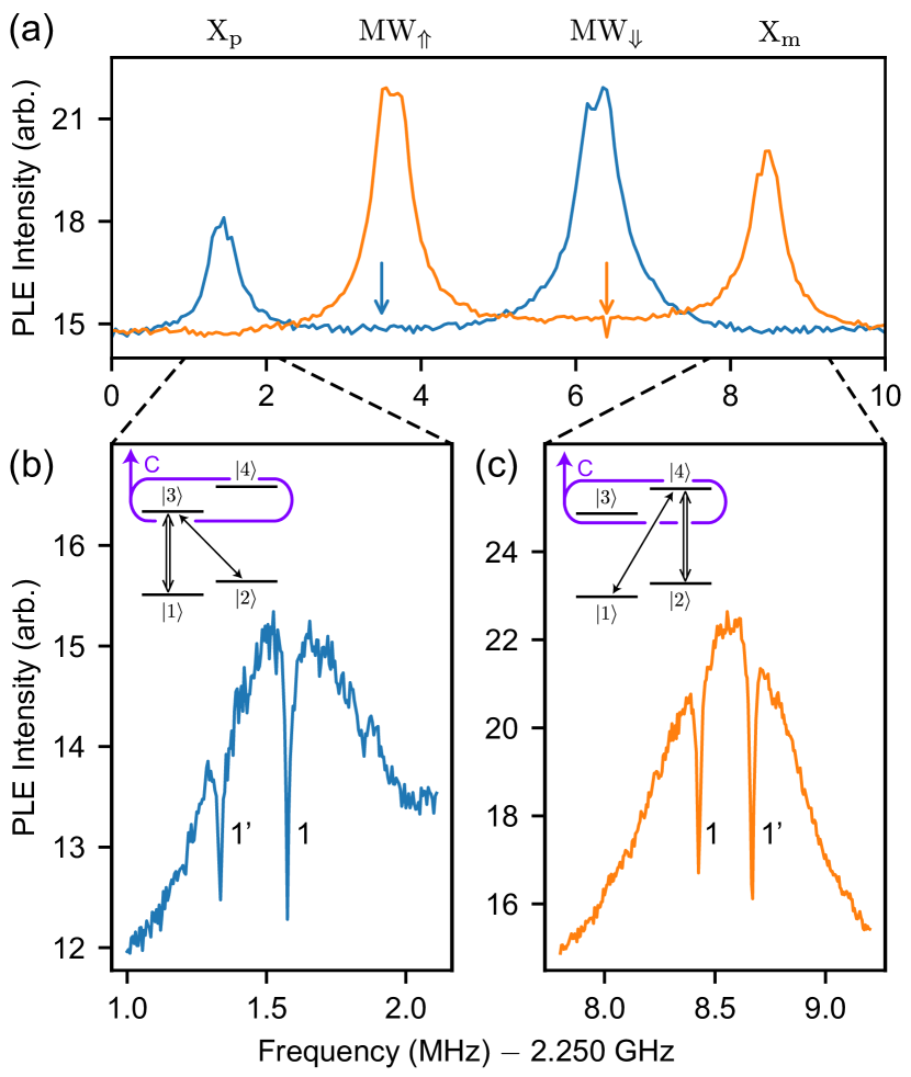
A ‘readout’ laser resonant with C1 selects these two optically degenerate subsets for ODMR spectroscopy. In the absence of any additional field the readout simply pumps these two optically degenerate orientational subsets into the electron spin state and this hyperpolarized ensemble does not fluoresce. Adding a single pump MW field that selects only one of the two hyperfine split states is still insufficient to prevent hyperpolarization, instead pumping the system to whichever of hyperfine states , remains unaddressed. In these ODMR measurements a MW ‘pump’ is set resonantly with one of the four available MW transitions and a second MW ‘probe’ scans over all four transitions. Continuous photoluminescence is detected when hyperfine states and are separately addressed by the MW fields. The ODMR spectra in Fig. 3(a) show two resonances per pump frequency. As expected resonances involving the ‘forbidden’ Xp,m are possible, but weaker and narrower than resonances with only MW⇓,⇑ (linewidths of 462(13), 506(9), 698(8) and 583(7) kHz respectively).
CPT is evident in each of the two possible MW configurations, shown inset to Fig. 3(a). When the MW fields are in two-photon resonance CPT produces a dark state superposition of and that does not couple to the readout laser. Higher resolution ODMR spectra in the region of the two-photon resonances, Fig. 3(b) and (c), show CPT luminescence dips with () kHz linewidth—significantly narrower than the ODMR lines. For each configuration in Fig. 3 there are two dark resonances, one for each of the distinct orientational subsets 1 and 1’ and separated by kHz, below the inhomogeneous linewidth and unresolvable by above-band PL. The low-power CPT linewidths are nuclear spin coherence limited, which is already known to be longer than s at this temperature [36]. However, at the microwave powers required to produce sufficient luminescence signal these CPT linewidths are broadened by the microwave Rabi frequencies , .
The observed ODMR and CPT profiles in Fig. 3 are the sum of fluorescence from the two near-degenerate orientational sub ensembles 1 and 1’, in proportion determined by relative concentration and dipole orientation. The precise ODMR peak associated with each ensemble is unknown. When one ensemble is in two-photon dark resonance, fluorescence from the remaining out-of-resonance ensemble is still present, with the effect that neither CPT dip apparently achieves complete fluorescence extinction as expected in the ideal low-power case.
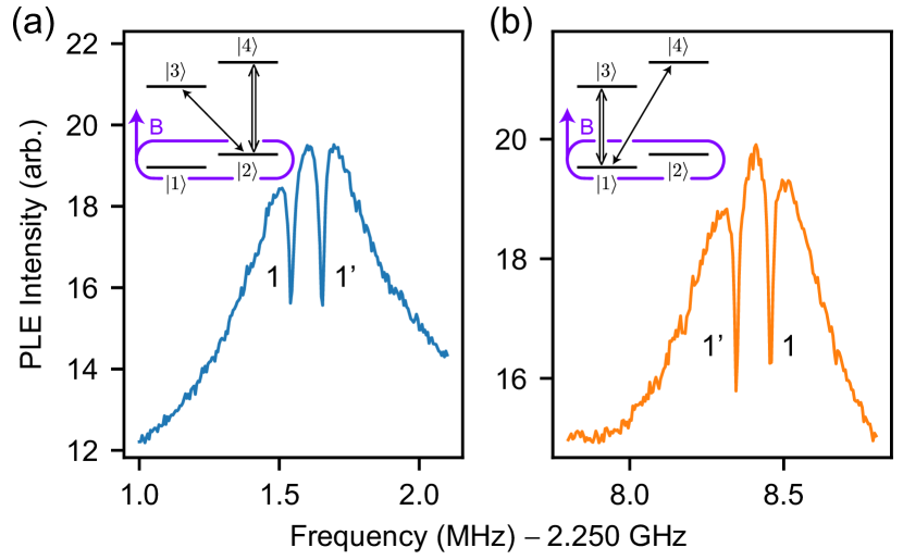
Optically pumping transition C empties states and , rapidly destroying any coherence , where is the density matrix of the centre, and power broadening the MW transitions. However the choice to read using optical transition C is arbitrary, and we can invert the system to achieve two-photon coherence via the less common V scheme. Choosing transition B instead empties and and removes coherence . This configuration sustains nuclear spin coherences of the hyperfine manifold, and we therefore expect CPT in V two-photon resonance, as shown in Fig. 4. The V CPT linewidths are kHz, identical to the case. The pump-probe MW frequency difference at each or V CPT condition determines effective hyperfine constants MHz and MHz for the 1 and 1’ sub-ensembles, respectively.
Dark CPT steady states decouple from the two fields in either or V configurations and cause a corresponding EIT window in the ensemble absorption. Absorption and dispersion manipulation by such electromagnetically induced transparency (EIT) is the operational principle of EIT quantum memories. In Section VI we consider the prospects for centre EIT memories (both optical and microwave), but first we perform one final preparatory measurement. In the same or V configuration, but in the limit of increasing pump power, the CPT window transitions to an Autler-Townes split transition, which is itself the basis of an Autler-Townes quantum memory.
V Autler-Townes splitting
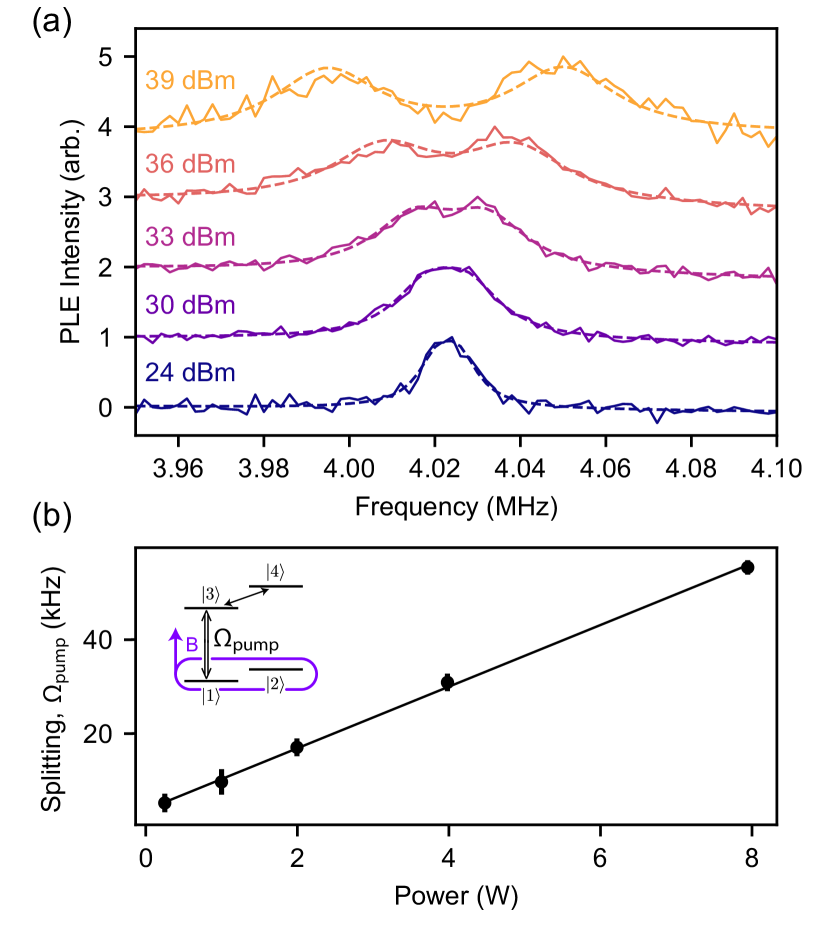
The operational bandwidth of EIT quantum memories is limited by the two-photon transition linewidth. Autler-Townes (AT) quantum memories utilize selective absorption by the spectrally distinct AT-split dressed states of a single transition to circumvent this limit [11]. With a modified ODMR scheme we can observe AT splitting of MW transitions in the same ensemble. For this measurement a slightly smaller magnetic field is chosen, mT along the [110] axis of the sample.
AT dressed states are split by the pump Rabi frequency . Rabi frequencies fitted to the CPT notches above, and observed by EPR with the same apparatus [36], indicate that attainable AT splittings MHz will not be clearly resolved with the ODMR schemes above. Instead, we apply an alternative ODMR scheme in which a radio frequency (RF) probe field scans over one of the NMR transitions. By this method we isolate a single sub-ensemble and achieve ODMR linewidths narrow enough to measure the transition to AT splitting as increases. Figure 5(a) shows ODMR spectra of the transition – as the MW power resonant with MW⇑ increases. The RF probe field is swept across the nuclear transition between states and . As the MW pump power increases, the RF resonances split by , the microwave Rabi frequency. We measure AT splitting up to kHz, demonstrating the basic mechanism required for microwave AT quantum memories. Splitting is limited in this case by the available MW power and inefficient resonator design. Larger splittings for improved optical and MW memory bandwidths are possible. In the following section we compare EIT and AT memory models to assess the prospects of centre memories for microwave and optical fields, and determine the optimal bandwidth for operating centre memories at feasible optical depths.
VI Free-space optical memory
The coherence times of the centre electron and nuclear spins, ms and s respectively, are appealing for quantum memory in either optical quantum networks or quantum processors. It remains to determine which of the many quantum memory schemes are best suited to the optical and microwave properties of centre ensembles determined in the literature and in the measurements above. Storage of a weak signal (i.e., probe) pulse using a relatively strong control field in a -type system has been studied using different protocols such as EIT, off-resonant Raman, and ATS [62, 1, 63, 11].
Keeping in mind that the nuclear splitting is not optically resolvable, there are four optical transitions per centre orientation that can be addressed individually and formed into two possible optical configurations addressing the electron spin coherence. In the ideal lifetime-limited case a centre optical quantum memory could directly address the longer-lived nuclear spin coherence, as in the MW memory proposal below, for storage times beyond s. However even the electron spin coherence time of ms is sufficient for a basic repeater demonstrations and swapping between the electron and nuclear spins is possible.
In this section we consider theoretically the -type system comprising two long-lived ground states and that are optically connected to a common excited state . We assume both electron and nuclear spins are initially polarized. We then use a strong control field with the Rabi frequency of in resonance with the optical transition , to store a weak signal pulse coupled to the transition (see Fig. 1).
Based on the optical depth measurement performed in Section III, centre ensembles could be made with optical depth sufficient for resonant optical quantum memory schemes given feasible concentration improvements. However, absent cavity-enhanced absorption, even these optical depths are insufficient for off-resonant schemes including gradient echo memory (GEM). Resonant memory schemes that efficiently utilize the available optical depth are best suited to near-term centre ensembles. In the following subsections we consider in detail the prospects of EIT and ATS free-space optical quantum memory schemes. Although centre ensembles exhibit optical inhomogeneous broadening of at least 33 MHz [36], throughout this analysis we consider spectral tailoring of the ensemble bounded from below by the homogeneous linewidth . Therefore, we neglect the effect of inhomogeneous broadening in our estimations.
VI.1 EIT Memory
In the EIT protocol, ramping down the control field power gradually to zero allows the adiabatic transfer of signal coherence to the spin-wave mode. EIT can be implemented effectively in both narrowband, i.e. , and broadband, i.e. , signal regimes where is the bandwidth of the signal at full-width half-maximum, and is the linewidth of the signal transition. However, this protocol is best suited for the narrowband regime where control field optimization is achievable at any optical depth. Eliminating signal absorption and maintaining adiabatic evolution with a broad transparency window requires both a very large optical depth and a strong control field [64, 65].
In general, EIT efficiency optimization is achievable through control field and/or signal pulse optimization [66, 67, 68]. The consistency of these optimization methods has been demonstrated in Ref. [69]. In the narrowband regime and for , control field optimization is achievable by keeping the process adiabatic while satisfying the condition , where is the group delay and is the signal time at FWHM [65]. Considering the probe field with a Gaussian temporal profile, the control optical Rabi frequency should therefore satisfy the condition .
For the centre with , corresponding to feasible near-term optical depths as discussed in Section III, the maximum achievable efficiency of the EIT protocol for the forward retrieval can be estimated as [69]. The memory efficiency for the backward propagation depends on the ground states splitting (as the non-zero splitting breaks the conservation of momentum in backward retrieval [66]). Therefore, for a non-zero splitting, the backward efficiency could be lower than the efficiency of the forward retrieval unless we make where is the length of the medium and is the speed of light.
This EIT memory efficiency estimate applies for short storage times. Reduction of the efficiency due to the spin decoherence can be taken into account by adding a term to the efficiency during the storage time [69, 66]. Other imperfections such as four-wave mixing [69, 70] may further reduce the experimentally achievable efficiency.
VI.2 ATS Memory
Unlike the EIT protocol, which relies on the adiabatic elimination of the atomic polarization mode, in ATS memory polarization mediates the non-adiabatic coherence exchange between the signal pulse and spin modes. In the broadband regime, ATS is less demanding in terms of technical requirements such as optical depth and control field power compared to the EIT memory. However, in the narrowband regime, the efficiency of the ATS memory is close to zero as the average coherence time of the transitions in resonance with the signal and control fields becomes shorter than the interaction time (i.e., signal pulse duration).
Assuming the system is initially prepared in the state , we can use dynamically controlled ATS lines produced by a strong control field that drives the – transition to absorb a weak signal pulse in resonance with the – transition [11]. Absorption of the signal pulse by ATS peaks (with a peak separation equal to the control Rabi frequency) will then map its coherence to a collective state between and (i.e., polarization mode), which subsequently evolves into a collective spin-excitation between the ground states. After the write (i.e., storage) process, we abruptly switch the control field off to trap the coherence, wait for storage time, and turn it on again for the read-out (i.e., retrieval) process. Using the control-field optimization, one can increase the spectral overlap between the ATS peaks separation and the signal bandwidth to maximize the signal pulse absorption. Here, the control-field optimization requires the control pulse area for both write and read stages to be [65]. Using the ATS memory protocol for the centre, a relatively high efficiency is achievable for broadband light storage and retrieval.
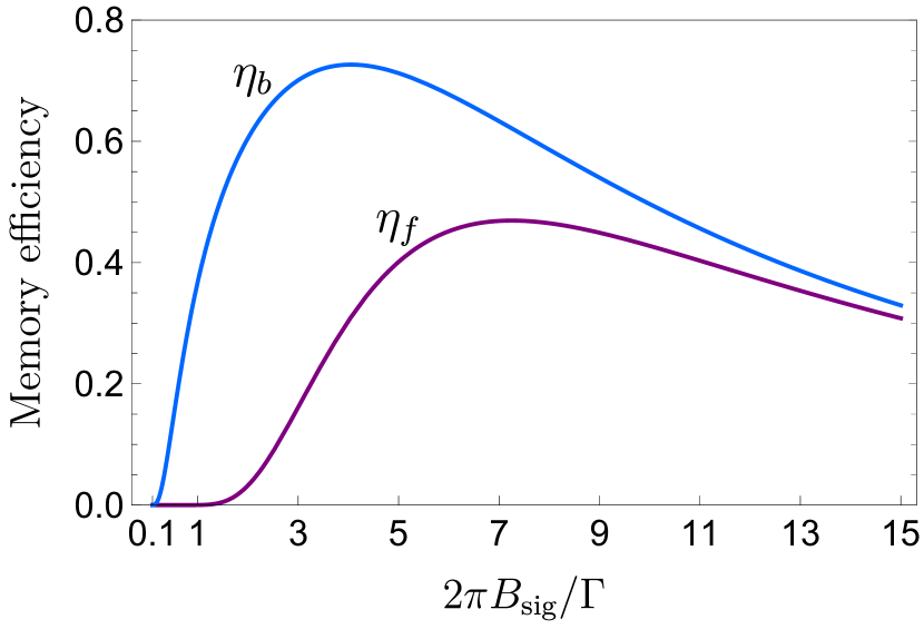
In Ref [71], ATS memory efficiency in the free space has been discussed in terms of the ATS factor (or equivalently ). As shown in Fig.6, for the centre with , the maximum efficiency of () for () is achievable in the backward (forward) propagation. For the optical memory, assuming MHz [45], these correspond to the Rabi frequency of and MHz for the backward and forward modes, respectively.
VII Microwave memory
We now turn our attention to centre prospects for MW quantum memories. In Sections IV and V we have measured coherent MW interactions in centre ensembles from the CPT to AT regimes. MW AT splitting such as we observed is a precursor to the demonstration of a -ATS MW memory. We will treat such an ATS memory theoretically to determine the prospects of MW memories with near term centre ensembles. For this study of the MW ATS memory we choose one of the two possible MW schemes shown in Section IV, assigning and as ground states and , respectively, and as excited state . We begin with an initial state , and use dynamically controlled ATS lines produced by a control field, as observed in Section V, to store a signal field resonant with the MW⇑ transition (see Fig.1). So that the coherence of the signal pulse is mapped into the collective nuclear spin excitations of the atoms. The theoretical treatment from Ref. [71] applies to the ATS MW memory as well as the optical memory considered above. For this case lower MW transition linewidths, as measured in Section IV, yield lower for the MW ATS memory.
However in general the weakness of magnetic dipole transitions requires a MW resonator to enhance the MW-ensemble coupling strength. To describe this resonantly enhanced interaction we can use the cavity input-output formalism i.e, , and Heisenberg equations of motion [11, 72]
| (2) | ||||
where and are the polarization and spin-wave operators, is the cavity field which we assume can be adiabatically eliminated, is the cavity decay rate, is the decoherence rate of the polarization mode and is the time-dependent light-matter coupling per emitter and is the number of atoms in the ensemble. Note that here we have ignored the Langevin noise operators (i.e., the incoming noise is vacuum) and once again assumed the spin-wave decoherence rate is negligible as per Section VI.
To estimate the overall efficiency of the memory in the presence of a resonator, we follow the same optimal scheme as in Ref [72] for the non-adiabatic or fast limit , where is the cooperativity parameter . The overall efficiency is , the product of the optimal storage efficiency (average ratio of stored excitations to incoming photons) and the optimal retrieval efficiency (average ratio of re-emitted photons to stored excitations). In the optimal regime, we compute the retrieval efficiency as
| (3) |
where is the effective time elapsed during the retrieval process. For simplicity, it is assumed that the retrieval process starts at rather than at some time where is the duration of the signal, and that and . It has been shown that using the optimal strategy the storage and retrieval efficiencies are analogous [73, 74, 72]. Hence, in the optimal regime, the overall efficiency can be estimated
| (4) |
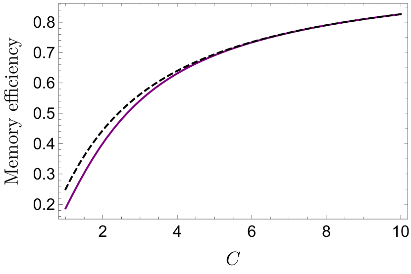
In deriving Eq.4, it is assumed that during the retrieval process all spin mode excitations have been evolved back to the polarization mode (i.e., no excitations are left in the spin mode). For fixed and finite values of the effective times, as the cavity cooperativity increases, the exponentially decaying terms of the Eq.4 go to zero, and hence, the first term dominates. Equivalently, in Eq.3, if we initially assume such that no excitations are left in the T ensemble i.e., , the optimal retrieval efficiency reduces to and the overall efficiency becomes (see Fig.7) [72]. With this maximum possible efficiency, one can store photons with where the polarization decay rate is negligible.
From this analysis we can see that resonator cooperativities of order are required to exceed % memory efficiency with a centre ensemble. Although we have introduced them in the context of the MW memory scheme, Eqs.2 apply to resonantly enhanced optical memories as well. In the following section we will propose to combine resonantly enhanced MW and optical memories to realize a centre MW to optical transducer with centre ensembles.
VIII Microwave-to-optical transduction
Motivated by the optical and microwave memory performance estimates above, we will now look at combining the capabilities to form a centre ensemble microwave-to-optical transducer that stores MW photons as spin-wave excitations and recalls them optically. For this operation we will consider both resonantly enhanced optical and microwave ATS memories.
Transduction may be achieved by way of two schemes, optical and microwave, addressing the same spin coherence. If this can not be achieved, it is necessary to transfer the coherence by an intermediate step. In the following, we elaborate on three possible approaches.
First, we may consider the MW and optical schemes set out in Section VI and Section VII. The MW configuration utilizes the long-lived nuclear spin coherence , however, as discussed in Section VI, the hyperfine splitting between and is not optically resolved in centre ensembles measured to date. Transduction from this microwave interface to an optical field using the same optical scheme we utilized in Section VI for an optical AT memory requires one to (i) store MW photons in resonance with the transition as nuclear spin-wave excitations between the states and , (ii) transfer the nuclear spin wave to an electron spin wave and (iii) recall the stored pulse using a control field in resonance with the optical transition . Transferring coherence between the nuclear and electron spin waves (step (ii)) requires only coherent control of the centre ground states, which has already been demonstrated over ensembles in Ref. [36].
Alternatively, one may consider schemes that avoid step (ii) above. One option is to use the electron spin for MW storage via a different configuration i.e. and as the ground states, and as the excited state. This configuration allows us to store MW photons in resonance with the – transition while the control field is resonant with the – transition. Note that the decoherence rate of the – and – transitions are comparable. In general this results in ATS line broadening and reduced efficiency [11]. However, in the limit that electron spin coherence time is very long, as it is in the centre [36] such ATS line broadening is negligible.
Finally, the transfer step is unnecessary when the hyperfine splitting of the nuclear spin wave is optically resolved. For example, in a scheme that utilizes larger hyperfine splittings due to nuclear spins at the carbon sites in 13C isotopic variants of [36], at higher magnetic fields, or by improving the optical linewidth such that the hydrogen hyperfine splitting is resolved. This way one can consider and as the joint ground states, and and as the excited state of the MW and optical systems, respectively.
VIII.1 Transduction efficiency and fidelity
Optimal efficiency of the transducer, where MW and optical transitions are coupled to the respective cavities, can be estimated using the same optimal strategy as for the ATS memory except that there is now an additional mode mismatch factor that should be taken into account. As a result, the overall efficiency would be . The mode mismatch factor depends on the design (geometry) of the cavities. In the ideal case, where all atoms are placed in the maximum of both optical and MW fields, the mode mismatch factor can reach unity. In this case and for , the optimal efficiency of the transducer is estimated as , where and are the cooperativity of the MW and optical cavities, repetitively.
The other metric to quantify the quality of transduction is the overlap between the transduced signal and the transduced noises. We refer to this measure as the transduction fidelity. In order to compute the fidelity, one could solve the system dynamics by taking several important imperfections such as spin decoherence, microwave thermal photons, and inhomogeneous broadening into account to determine the fidelity. As discussed before, inhomogeneous broadening can be dealt with by spectral tailoring. Therefore, here we only consider the thermal photons in the microwave cavity. Spin decoherence is also negligible given that the process can be much faster than the spin coherence times [36]. For this calculation, we consider a transduction system consisting of and as the ground states, and and as the excited state of the microwave and optical subsystems, respectively.
The initial microwave thermal occupation is estimated to be with mK and GHz [36] which is the splitting between and . Since the initial microwave photon occupation is quite small, and it does not affect the quantum system dynamics significantly, we can treat it separately from the signal. The fidelity can be computed using the signal-to-noise ratio (SNR) [28]:
| (5) |
Given that the thermal noise and signal can be treated independently, it is valid to compute the SNR even before the transduction process starts. In this way, the SNR is given by:
| (6) |
where is the mean occupation of signal in microwave cavity. For a single-photon signal, , where is the microwave cavity decay rate. This is valid in the regime that . Given that , the fidelity shown in Eq.(5) can be simplified as:
| (7) |
Since we are interested in the case where the transduction efficiency is maximized, can be expressed as . Hence, in the regime of maximum efficiency, the fidelity is explicitly given by:
| (8) |
Clearly, as the cavity cooperativity increases, the fidelity increases, and the efficiency also increases as shown in Fig. 7.
The other way to compute the fidelity is to estimate the SNR after the transduction, which should be equivalent to the approach discussed above. In this way, we can model the microwave thermal photons as dark counts [75]. The dark count rate is given by with the transduction efficiency and the average rate of thermal photons . It describes the effective number of photons emitted as background noise in the optical cavity per unit of time. The probability distribution associated with this dark count rate is given by a Poisson distribution where is the number of dark counts and is the total transduction time. Thus, this time can also be written as .
Then, for a single-photon transduction, the SNR takes the following form:
| (9) |
where is the mean number of dark counts. Specifically, at a given time the SNR becomes:
| (10) |
where is the mean number of dark counts that follow the Poisson distribution. It can be further simplified as . In the regime of the maximum efficiency, , we recover , which leads to the fidelity shown in Eq.(8).
IX Discussion
The centre appears to combine several properties appealing for both microwave and quantum memories, and transduction between them, including long lived spins and telecom optical emission. We have considered possible quantum memory and transduction schemes for ensembles of centres, and performed preliminary measurements with ensembles in to establish properties informing memory and transduction device design.
Absorption measurements indicate a resonant optical depth of in a narrow-linewidth ensemble. Cautiously forecasting a small improvement over centre concentrations that have already been demonstrated in devices, we project that an optical depth of with a similar sample is possible. This optical depth is sufficient for efficient optical quantum memory by EIT or ATS with estimated a memory efficiency as high as .
In addition to the potential for optical memory, the centre’s optical ground state spin structure features and V configurations suitable for storing MW fields. We demonstrated these configurations by ODMR spectroscopy, and measured CPT windows in and V configurations as a precursor to an EIT memory for MW fields. Fluorescence SNR requirements prohibit us from reaching the low-power limit, but even so we measured CPT linewidths of kHz, significantly below the ODMR linewidth, and resolved orientation sub-ensembles that were degenerate to MW ODMR precision. We demonstrated microwave ATS up to kHz splitting. We then discussed a cavity-enhanced MW memory protocol and arrived at an efficiency estimate as a function of cavity cooperativity. In particular, MW memory efficiencies of greater than are possible for .
In general, the operation of MW and optical centre quantum memories can be combined to transduce between the microwave and optical fields. Transduction requires either (i) an optical quantum memory addressing the nuclear spin coherence , (ii) a microwave memory addressing an electron spin coherence such as via an NMR control field, or (iii) coherent transfer between and at an intermediate stage. (iii) requires only the coherent control of ensembles that has already been experimentally demonstrated [36]. Furthermore, (i) is within reach of schemes utilizing the known 13C centre variants.
We proposed a transduction protocol where both microwave and optical transitions are coupled to resonators, and discussed the efficiency and fidelity of the system. Mutually compatible MW and optical cavities with would yield microwave to optical transduction efficiencies of . Necessary future work includes further improving ensemble concentrations, and engineering optical and microwave resonators meeting these metrics, but an in-principle centre transduction demonstration could be achieved with designs available in the literature.
We have demonstrated the potential of this new spin-photon platform for quantum memory, and identified pathways towards efficient microwave-to-optical transduction with centres. Further developing and transplanting this approach into on-chip devices, for example with integrated silicon photonic resonators combining moderate mode confinement and high quality factors, would yield an on-chip spin-photon interface for quantum memories and microwave to optical transducers. These devices could network directly between quantum information platforms that share the same technologically and commercially advanced silicon chip platform (including superconducting qubits, quantum dots, trapped ions, and silicon impurity spins) and the telecom optical fibres of a global quantum internet.
Acknowledgements
This work was supported by the Natural Sciences and Engineering Research Council of Canada (NSERC), the New Frontiers in Research Fund (NFRF), the National Research Council (NRC) of Canada through its High-Throughput Secure Networks (HTSN) challenge program, the Canada Research Chairs program (CRC), the Canada Foundation for Innovation (CFI), the B.C. Knowledge Development Fund (BCKDF), and the Canadian Institute for Advanced Research (CIFAR) Quantum Information Science program. D.B.H is supported by the Banting Fellowship program.
The 28Si samples used in this study were prepared from the Avo28 crystal produced by the International Avogadro Coordination (IAC) Project (2004–2011) in cooperation among the BIPM, the INRIM (Italy), the IRMM (EU), the NMIA (Australia), the NMIJ (Japan), the NPL (UK), and the PTB (Germany). We thank Alex English of Iotron Industries for assistance with electron irradiation.
APPENDIX A: SAMPLE PREPARATION
All measurements are performed on one of two crystals, previously described in Ref. [36]. These have been purified to 99.995% isotope proportion by the Avogadro project and then electron irradiated and thermally annealed to produce . In addition to isotopic purity these samples have low chemical impurity, with less than oxygen/cm3. centres are formed from naturally present low-level carbon impurities, which differ between the two samples. The sample used for absorption measurements has carbon/cm3, the sample used for CPT and ATS measurements has carbon/cm3.
APPENDIX B: METHODS
Cryogenics
The samples are loosely mounted in a liquid Helium immersion dewar such that the crystal is not strained. The temperature of the Helium-4 bath is adjusted between – K by pressure control.
Photoluminescence spectra
The sample is illuminated with an above-bandgap nm laser and the resulting broadband photoluminescence is directed into a Bruker IFS 125 HR Fourier Transform infrared (FTIR) spectrometer with a CaF2 beam splitter and liquid nitrogen cooled Ge photodetector.
Absorption measurement
The sample is illuminated along its longest side by a broadband light source with beam size smaller than the sample cross section. Light passes through the sample and two cryostat windows before being directed into the Bruker FTIR spectrometer. The light source spectrum is free of structure in the vicinity of the centre absorption lines and is removed by subtracting a linear fit about the absorption dip location.
Photoluminescence excitation
Photoluminescence excitation spectra are recorded by scanning a narrow, tunable laser over the TX0 ZPL and detecting lower energy photons emitted into the TX phonon sideband. Resonant excitation is performed with a Toptica DL100 tunable diode laser. The optical power is amplified up to mW with a Thorlabs BOA1017P and the beam is expanded to diameter – mm. Non-resonant excitation light due to spontaneous emission in the laser and amplifier is removed by a combination of an Edmund Optics 87-830 nm and Iridian Spectral Technologies DWDM nm bandpass filters. The two filters are tilted so as to tune them onto the TX0 resonance.
Stray excitation light is removed from the detection path by two Semrock BLP02-1319R-25 nm longpass rejection filters, which in fact block the excitation light at TX0 with OD at normal incidence, but pass light with wavelength longer than nm. A () nm bandpass filter further selects a detection window in the TX phonon sideband that excludes a silicon Raman replica of the pump laser at nm. The fluorescence rate in this detection window is measured by an IDQuantique ID230 avalanche photodiode with 25% quantum efficiency.
Optically Detected Magnetic Resonance
Magnetic resonance experiments are performed with the sample in an adjustable magnetic field applied by an iron core electromagnet within the PLE apparatus as described above. The sample is held at the centre of a split-ring resonator with a resonant frequency of GHz and MHz bandwidth. MW signals from by two SRS SG384 and SG386 signal generators are combined with a ZB2PD-63-S+ power splitter and then amplified up to 1W of power by ZHL-16W-43-S+ and ZHL-1-2W+ amplifiers as required.
References
- Lvovsky et al. [2009] A. I. Lvovsky, B. C. Sanders, and W. Tittel, Optical quantum memory, Nature Photonics 3, 706 (2009).
- Briegel et al. [1998] H.-J. Briegel, W. Dür, J. I. Cirac, and P. Zoller, Quantum repeaters: the role of imperfect local operations in quantum communication, Physical Review Letters 81, 5932 (1998).
- Childress et al. [2005] L. I. Childress, J. M. Taylor, A. Sørensen, and M. D. Lukin, Fault-tolerant quantum repeaters with minimal physical resources and implementations based on single-photon emitters, Physical Review A 72, 052330 (2005).
- Sangouard et al. [2011] N. Sangouard, C. Simon, H. de Riedmatten, and N. Gisin, Quantum repeaters based on atomic ensembles and linear optics, Reviews of Modern Physics 83, 33 (2011).
- Asadi et al. [2018] F. Kimiaee Asadi, N. Lauk, S. Wein, N. Sinclair, C. O’Brien, and C. Simon, Quantum repeaters with individual rare-earth ions at telecommunication wavelengths, Quantum 2, 93 (2018).
- Kimble [2008] H. J. Kimble, The quantum internet, Nature 453, 1023 (2008).
- Gouzien and Sangouard [2021] E. Gouzien and N. Sangouard, Factoring 2048-bit rsa integers in 177 days with 13 436 qubits and a multimode memory, Phys. Rev. Lett. 127, 140503 (2021).
- Fleischhauer et al. [2005] M. Fleischhauer, A. Imamoglu, and J. P. Marangos, Electromagnetically induced transparency: Optics in coherent media, Reviews of modern physics 77, 633 (2005).
- Afzelius et al. [2009] M. Afzelius, C. Simon, H. de Riedmatten, and N. Gisin, Multimode quantum memory based on atomic frequency combs, Physical Review A 79, 052329 (2009).
- Kraus et al. [2006] B. Kraus, W. Tittel, N. Gisin, M. Nilsson, S. Kröll, and J. I. Cirac, Quantum memory for nonstationary light fields based on controlled reversible inhomogeneous broadening, Physical Review A 73, 020302(R) (2006).
- Saglamyurek et al. [2018a] E. Saglamyurek, T. Hrushevskyi, A. Rastogi, K. Heshami, and L. J. LeBlanc, Coherent storage and manipulation of broadband photons via dynamically controlled Autler–Townes splitting, Nature Photonics 12, 774 (2018a).
- Ma et al. [2021] Y. Ma, Y.-Z. Ma, Z.-Q. Zhou, C.-F. Li, and G.-C. Guo, One-hour coherent optical storage in an atomic frequency comb memory, Nature communications 12, 1 (2021).
- Hedges et al. [2010] M. P. Hedges, J. J. Longdell, Y. Li, and M. J. Sellars, Efficient quantum memory for light, Nature 465, 1052 (2010).
- Heshami et al. [2014] K. Heshami, C. Santori, B. Khanaliloo, C. Healey, V. M. Acosta, P. E. Barclay, and C. Simon, Raman quantum memory based on an ensemble of nitrogen-vacancy centers coupled to a microcavity, Physical Review A 89, 040301(R) (2014).
- Guo et al. [2019] J. Guo, X. Feng, P. Yang, Z. Yu, L. Chen, C.-H. Yuan, and W. Zhang, High-performance raman quantum memory with optimal control in room temperature atoms, Nature communications 10, 1 (2019).
- Katz and Firstenberg [2018] O. Katz and O. Firstenberg, Light storage for one second in room-temperature alkali vapor, Nature communications 9, 1 (2018).
- Zhang et al. [2009] R. Zhang, S. R. Garner, and L. V. Hau, Creation of long-term coherent optical memory via controlled nonlinear interactions in bose-einstein condensates, Physical Review Letters 103, 233602 (2009).
- Saglamyurek et al. [2021] E. Saglamyurek, T. Hrushevskyi, A. Rastogi, L. W. Cooke, B. D. Smith, and L. J. LeBlanc, Storing short single-photon-level optical pulses in bose–einstein condensates for high-performance quantum memory, New Journal of Physics 23, 043028 (2021).
- Lauk et al. [2020] N. Lauk, N. Sinclair, S. Barzanjeh, J. P. Covey, M. Saffman, M. Spiropulu, and C. Simon, Perspectives on quantum transduction (2020).
- Vandersypen and Eriksson [2019] L. M. Vandersypen and M. A. Eriksson, Quantum computing with semiconductor spins, Physics Today 72, 38 (2019).
- Xue et al. [2022] X. Xue, M. Russ, N. Samkharadze, B. Undseth, A. Sammak, G. Scappucci, and L. M. Vandersypen, Quantum logic with spin qubits crossing the surface code threshold, Nature 601, 343 (2022).
- Tu et al. [2022] H. T. Tu, K. Y. Liao, Z. X. Zhang, X. H. Liu, S. Y. Zheng, S. Z. Yang, X. D. Zhang, H. Yan, and S. L. Zhu, High-efficiency coherent microwave-to-optics conversion via off-resonant scattering, Nature Photonics 2022 16:4 16, 291 (2022).
- Higginbotham et al. [2018] A. P. Higginbotham, P. Burns, M. Urmey, R. Peterson, N. Kampel, B. Brubaker, G. Smith, K. Lehnert, and C. Regal, Harnessing electro-optic correlations in an efficient mechanical converter, Nature Physics 14, 1038 (2018).
- Fan et al. [2018] L. Fan, C.-L. Zou, R. Cheng, X. Guo, X. Han, Z. Gong, S. Wang, and H. X. Tang, Superconducting cavity electro-optics: a platform for coherent photon conversion between superconducting and photonic circuits, Science advances 4, eaar4994 (2018).
- Vogt et al. [2019] T. Vogt, C. Gross, J. Han, S. B. Pal, M. Lam, M. Kiffner, and W. Li, Efficient microwave-to-optical conversion using rydberg atoms, Physical Review A 99, 023832 (2019).
- O’Brien et al. [2014] C. O’Brien, N. Lauk, S. Blum, G. Morigi, and M. Fleischhauer, Interfacing superconducting qubits and telecom photons via a rare-earth-doped crystal, Physical Review Letters 113, 063603 10.1103/PhysRevLett.113.063603 (2014).
- Li et al. [2017] B. Li, P.-B. Li, Y. Zhou, S.-L. Ma, and F.-L. Li, Quantum microwave-optical interface with nitrogen-vacancy centers in diamond, Physical Review A 96, 032342 (2017).
- Asadi et al. [2022] F. Kimiaee Asadi, J.-W. Ji, and C. Simon, Proposal for transduction between microwave and optical photons using er 167-doped yttrium orthosilicate, Physical Review A 105, 062608 (2022).
- Fernandez-Gonzalvo et al. [2015] X. Fernandez-Gonzalvo, Y.-H. Chen, C. Yin, S. Rogge, and J. J. Longdell, Coherent frequency up-conversion of microwaves to the optical telecommunications band in an Er:YSO crystal, Physical Review A 92, 062313 (2015).
- Soltani et al. [2017] M. Soltani, M. Zhang, C. Ryan, G. J. Ribeill, C. Wang, and M. Loncar, Efficient quantum microwave-to-optical conversion using electro-optic nanophotonic coupled resonators, Physical Review A 96, 043808 (2017).
- Stannigel et al. [2010] K. Stannigel, P. Rabl, A. S. Sørensen, P. Zoller, and M. D. Lukin, Optomechanical transducers for long-distance quantum communication, Physical review letters 105, 220501 (2010).
- Hisatomi et al. [2016] R. Hisatomi, A. Osada, Y. Tabuchi, T. Ishikawa, A. Noguchi, R. Yamazaki, K. Usami, and Y. Nakamura, Bidirectional conversion between microwave and light via ferromagnetic magnons, Physical Review B 93, 174427 (2016).
- Das et al. [2017] S. Das, V. E. Elfving, S. Faez, and A. S. Sørensen, Interfacing superconducting qubits and single optical photons using molecules in waveguides, Physical review letters 118, 140501 (2017).
- Williamson et al. [2014] L. A. Williamson, Y.-H. Chen, and J. J. Longdell, Magneto-Optic Modulator with Unit Quantum Efficiency, Physical Review Letters 113, 203601 (2014).
- Xie et al. [2021] T. Xie, J. Rochman, J. G. Bartholomew, A. Ruskuc, J. M. Kindem, I. Craiciu, C. W. Thiel, R. L. Cone, and A. Faraon, Characterization of Er3+:YV O4 for microwave to optical transduction, Physical Review B 104, 054111 (2021).
- Bergeron et al. [2020] L. Bergeron, C. Chartrand, A. T. K. Kurkjian, K. J. Morse, H. Riemann, N. V. Abrosimov, P. Becker, H.-J. Pohl, M. L. W. Thewalt, and S. Simmons, Silicon-Integrated Telecommunications Photon-Spin Interface, PRX Quantum 1, 020301 (2020).
- Higginbottom et al. [2022] D. B. Higginbottom, A. T. K. Kurkjian, C. Chartrand, E. R. MacQuarrie, J. R. Klein, N. R. Lee-Hone, J. Stacho, C. Bowness, L. Bergeron, A. DeAbreu, N. A. Brunelle, S. R. Harrigan, J. Kanaganayagam, M. Kazemi, D. W. Marsden, T. S. Richards, L. A. Stott, S. Roorda, K. J. Morse, M. L. W. Thewalt, and S. Simmons, Optical observation of single spins in silicon, Nature 607, 266 (2022).
- Cho et al. [2015] D. I. D. Cho, S. Hong, M. Lee, and T. Kim, A review of silicon microfabricated ion traps for quantum information processing (2015).
- Veldhorst et al. [2017] M. Veldhorst, H. G. Eenink, C. H. Yang, and A. S. Dzurak, Silicon CMOS architecture for a spin-based quantum computer, Nature Communications 8, 1 (2017).
- Arute et al. [2019] F. Arute, K. Arya, R. Babbush, D. Bacon, J. C. Bardin, R. Barends, R. Biswas, S. Boixo, F. G. S. L. Brandao, D. A. Buell, B. Burkett, Y. Chen, Z. Chen, B. Chiaro, R. Collins, W. Courtney, A. Dunsworth, E. Farhi, B. Foxen, A. Fowler, C. Gidney, M. Giustina, R. Graff, K. Guerin, S. Habegger, M. P. Harrigan, M. J. Hartmann, A. Ho, M. Hoffmann, T. Huang, T. S. Humble, S. V. Isakov, E. Jeffrey, Z. Jiang, D. Kafri, K. Kechedzhi, J. Kelly, P. V. Klimov, S. Knysh, A. Korotkov, F. Kostritsa, D. Landhuis, M. Lindmark, E. Lucero, D. Lyakh, S. Mandrà, J. R. McClean, M. McEwen, A. Megrant, X. Mi, K. Michielsen, M. Mohseni, J. Mutus, O. Naaman, M. Neeley, C. Neill, M. Y. Niu, E. Ostby, A. Petukhov, J. C. Platt, C. Quintana, E. G. Rieffel, P. Roushan, N. C. Rubin, D. Sank, K. J. Satzinger, V. Smelyanskiy, K. J. Sung, M. D. Trevithick, A. Vainsencher, B. Villalonga, T. White, Z. J. Yao, P. Yeh, A. Zalcman, H. Neven, and J. M. Martinis, Quantum supremacy using a programmable superconducting processor, Nature 574, 505 (2019).
- Pla et al. [2012] J. J. Pla, K. Y. Tan, J. P. Dehollain, W. H. Lim, J. J. L. Morton, D. N. Jamieson, A. S. Dzurak, and A. Morello, A single-atom electron spin qubit in silicon, Nature 489, 10.1038/nature11449 (2012).
- Wang et al. [2020] J. Wang, F. Sciarrino, A. Laing, and M. G. Thompson, Integrated photonic quantum technologies (2020).
- Irion et al. [1985] E. Irion, N. Burger, K. Thonke, and R. Sauer, The defect luminescence spectrum at 0.9351 eV in carbon-doped heat-treated or irradiated silicon, Journal of Physics C: Solid State Physics 18, 5069 (1985).
- Safonov et al. [1996] A. N. Safonov, E. C. Lightowlers, G. Davies, P. Leary, R. Jones, and S. Öberg, Interstitial-Carbon Hydrogen Interaction in Silicon, Phys. Rev. Lett. 77, 4812 (1996).
- MacQuarrie et al. [2021] E. R. MacQuarrie, C. Chartrand, D. B. Higginbottom, K. J. Morse, V. A. Karasyuk, S. Roorda, and S. Simmons, Generating T centres in photonic silicon-on-insulator material by ion implantation, New Journal of Physics 23, 103008 (2021).
- Dhaliah et al. [2022] D. Dhaliah, Y. Xiong, A. Sipahigil, S. M. Griffin, and G. Hautier, First-principles study of the T center in silicon, Physical Review Materials 6, L053201 (2022).
- Hilborn [1982] R. C. Hilborn, Einstein coefficients, cross sections, f values, dipole moments, and all that, American Journal of Physics 50, 982 (1982).
- Murata et al. [2011] K. Murata, Y. Yasutake, K. I. Nittoh, S. Fukatsu, and K. Miki, High-density G-centers, light-emitting point defects in silicon crystal, AIP Advances 1, 032125 (2011).
- Rotem et al. [2007] E. Rotem, J. M. Shainline, and J. M. Xu, Enhanced photoluminescence from nanopatterned carbon-rich silicon grown by solid-phase epitaxy, Applied Physics Letters 91, 051127 (2007).
- Green [2008] M. A. Green, Self-consistent optical parameters of intrinsic silicon at 300 K including temperature coefficients, Solar Energy Materials and Solar Cells 92, 1305 (2008).
- Markosyan et al. [2018] A. Markosyan, A. E. Shitikov, I. A. Bilenko, M. L. Gorodetsky, N. M. Kondratiev, and V. E. Lobanov, Billion Q-factor in silicon WGM resonators, Optica, Vol. 5, Issue 12, pp. 1525-1528 5, 1525 (2018).
- Asano et al. [2017] T. Asano, Y. Ochi, Y. Takahashi, K. Kishimoto, and S. Noda, Photonic crystal nanocavity with a Q factor exceeding eleven million, Optics Express 25, 1769 (2017).
- Arimondo and Orriols [1976] E. Arimondo and G. Orriols, Nonabsorbing atomic coherences by coherent two-photon transitions in a three-level optical pumping, Lettere Al Nuovo Cimento Series 2 17, 333 (1976).
- Gray et al. [1978] H. R. Gray, R. M. Whitley, and C. R. Stroud, Coherent trapping of atomic populations, Optics Letters 3, 218 (1978).
- Boller et al. [1991] K.-J. Boller, A. Imamoğlu, and S. E. Harris, Observation of electromagnetically induced transparency, Physical Review Letters 66, 2593 (1991).
- Alzetta et al. [1976] G. Alzetta, A. Gozzini, L. Moi, and G. Orriols, An experimental method for the observation of r.f. transitions and laser beat resonances in oriented Na vapour, Il Nuovo Cimento B Series 11 36, 5 (1976).
- Rakhmatullin et al. [1998] R. Rakhmatullin, E. Hoffmann, G. Jeschke, and A. Schweiger, Dark magnetic resonance in an electron-nuclear spin system, Physical Review A - Atomic, Molecular, and Optical Physics 57, 3775 (1998).
- Wei and Manson [1999] C. Wei and N. B. Manson, Observation of electromagnetically induced transparency within an electron spin resonance transition, Journal of Optics B: Quantum and Semiclassical Optics 1, 464 (1999).
- Childress and McIntyre [2010] L. Childress and J. McIntyre, Multifrequency spin resonance in diamond, Physical Review A - Atomic, Molecular, and Optical Physics 82, 033839 (2010).
- Novikov et al. [2015] S. Novikov, T. Sweeney, J. E. Robinson, S. P. Premaratne, B. Suri, F. C. Wellstood, and B. S. Palmer, Raman coherence in a circuit quantum electrodynamics lambda system, Nature Physics 2015 12:1 12, 75 (2015).
- Jamonneau et al. [2016] P. Jamonneau, G. Hétet, A. Dréau, J. F. Roch, and V. Jacques, Coherent Population Trapping of a Single Nuclear Spin under Ambient Conditions, Physical Review Letters 116, 043603 (2016).
- Lukin [2003] M. Lukin, Colloquium: Trapping and manipulating photon states in atomic ensembles, Reviews of Modern Physics 75, 457 (2003).
- Reim et al. [2010] K. Reim, J. Nunn, V. Lorenz, B. Sussman, K. Lee, N. Langford, D. Jaksch, and I. Walmsley, Towards high-speed optical quantum memories, Nature Photonics 4, 218 (2010).
- Wei et al. [2020] Y.-C. Wei, B.-H. Wu, Y.-F. Hsiao, P.-J. Tsai, and Y.-C. Chen, Broadband coherent optical memory based on electromagnetically induced transparency, Physical Review A 102, 063720 (2020).
- Rastogi et al. [2019] A. Rastogi, E. Saglamyurek, T. Hrushevskyi, S. Hubele, and L. J. LeBlanc, Discerning quantum memories based on electromagnetically-induced-transparency and autler-townes-splitting protocols, Physical Review A 100, 012314 (2019).
- Gorshkov et al. [2007a] A. V. Gorshkov, A. André, M. D. Lukin, and A. S. Sørensen, Photon storage in -type optically dense atomic media. ii. free-space model, Physical Review A 76, 033805 (2007a).
- Novikova et al. [2007] I. Novikova, A. V. Gorshkov, D. F. Phillips, A. S. Sørensen, M. D. Lukin, and R. L. Walsworth, Optimal control of light pulse storage and retrieval, Physical Review Letters 98, 243602 (2007).
- Novikova et al. [2008] I. Novikova, N. B. Phillips, and A. V. Gorshkov, Optimal light storage with full pulse-shape control, Physical Review A 78, 021802(R) (2008).
- Phillips et al. [2008] N. B. Phillips, A. V. Gorshkov, and I. Novikova, Optimal light storage in atomic vapor, Physical Review A 78, 023801 (2008).
- Lauk et al. [2013] N. Lauk, C. O’Brien, and M. Fleischhauer, Fidelity of photon propagation in electromagnetically induced transparency in the presence of four-wave mixing, Physical Review A 88, 013823 (2013).
- Saglamyurek et al. [2018b] E. Saglamyurek, T. Hrushevskyi, A. Rastogi, K. Heshami, and L. J. LeBlanc, Coherent storage and manipulation of broadband photons via dynamically controlled autler–townes splitting, Nature Photonics 12, 774 (2018b).
- Gorshkov et al. [2007b] A. V. Gorshkov, A. André, M. D. Lukin, and A. S. Sørensen, Photon storage in -type optically dense atomic media. i. cavity model, Physical Review A 76, 033804 (2007b).
- Gorshkov et al. [2007c] A. V. Gorshkov, A. André, M. Fleischhauer, A. S. Sørensen, and M. D. Lukin, Universal approach to optimal photon storage in atomic media, Physical review letters 98, 123601 (2007c).
- Heshami et al. [2012] K. Heshami, A. Green, Y. Han, A. Rispe, E. Saglamyurek, N. Sinclair, W. Tittel, and C. Simon, Controllable-dipole quantum memory, Physical Review A 86, 013813 (2012).
- Ji et al. [2022] J.-W. Ji, Y.-F. Wu, S. C. Wein, F. K. Asadi, R. Ghobadi, and C. Simon, Proposal for room-temperature quantum repeaters with nitrogen-vacancy centers and optomechanics, Quantum 6, 669 (2022).