Neutral Silicon Vacancy Centers in Diamond via Photoactivated Itinerant Carriers
Abstract
Neutral silicon vacancy (SiV0) centers in diamond are promising candidates for quantum network applications because of their exceptional optical properties and spin coherence. However, the stabilization of SiV0 centers requires careful Fermi level engineering of the diamond host material, making further technological development challenging. Here, we show that SiV0 centers can be efficiently stabilized by photoactivated itinerant carriers. Even in this nonequilibrium configuration, the resulting SiV0 centers are stable enough to allow for resonant optical excitation and optically detected magnetic resonance. Our results pave the way for on-demand generation of SiV0 centers as well as other emerging quantum defects in diamond.
Color centers in the solid state are actively explored as building blocks for quantum sensing and quantum information processing because of their exceptional spin and optical properties [1, 2, 3]. As atomic systems, they can exhibit narrow optical transitions and long spin coherence times. As solid state objects, they can be integrated into devices in a scalable manner. However, the solid state environment also leads to complicated charge dynamics. For example, impurities or dopants in the substrate [4, 5], optical illumination of photo-active impurities [6], and surface properties of the substrate [7, 8] can all impact the stability and the dynamics of the desired charge state. Using optical illumination to initialize the charge state is commonly deployed for various color centers, including nitrogen vacancy (NV) and silicon vacancy (SiV) centers in diamond [9, 10, 11]. However, the fidelity of the initialization is limited [12], and depends strongly on the microscopic details of the sample, especially when the centers are near the surface [13, 8]. New methods to control and stabilize particular charge states would enable many technological applications based on color centers.
Recently, it was shown that the charge state of color centers in diamond can be affected by optical illumination of nearby defects [14]. The optically activated itinerant carriers (holes and electrons) diffuse before they are captured, resulting in a non-local modification of the charge state distribution. Using itinerant carriers that are generated remotely avoids possible complications from ionization and recombination under direct illumination. This procedure has been demonstrated for both NV centers and SiV centers, and the effect has been attributed to optical ionization of nearby NV centers, SiV centers or substitutional nitrogen (P1 centers) [14, 15, 16, 17]. For NV centers, the negative charge state (NV-) captures holes efficiently, converting NV- to NV0 [16, 17]. For SiV centers, the negative charge state (SiV-) can be generated in a similar manner; however the nature of the charge state prior to conversion is disputed in part because of the lack of direct observation of the neutral silicon vacancy (SiV0) centers [15, 16].
In this work, we demonstrate stabilization of SiV0 centers in diamond via photoactivation of itinerant carriers. SiV0 centers are unstable in typical high purity diamonds because the Fermi level set by nitrogen impurities is above the charge transition point from the neutral to negative charge states [18], and high conversion to the neutral charge state has only been demonstrated in a limited number of boron doped diamonds [19], or through surface transfer doping in undoped diamond [20]. Here, instead of relying on careful preparation and doping of the diamond, we create a nonequilibrium charge state by utilizing the itinerant carriers generated from nearby defects upon optical illumination. We show that SiV- centers are capable of capturing photoactivated holes, which metastably converts them into SiV0 centers. We study the dynamics of carrier diffusion, the ionization of SiV0 under illumination, and the dependence of the dynamics on excitation wavelength. The wavelength dependence allows us to infer that dynamic charge state conversion of NV centers plays the major role in generating the itinerant carriers in our sample. The nonequilibrium SiV0 centers are stable both in the dark and under typical near-infrared (NIR) optical excitation, enabling resonant optical excitation and optically detected magnetic resonance (ODMR).
The sample studied in this work is a plasma chemical-vapor deposition grown sample doped with isotopically enriched 29Si during growth (Element Six). We estimate the NV- concentration to be 0.03 ppb and the SiV- concentration to be 30 ppb by comparing the photoluminescence signal to the signal of samples with known NV- and SiV- concentrations. The silicon concentration was determined from secondary ion mass spectrometry to be 0.8 ppm. The nitrogen concentration is below the detection limits of Fourier-transform infrared spectroscopy (upper bound of 300 ppb, Fig. S1 [21]), but is at least 9 ppb based on the native NV- concentration [22]. Experiments were conducted at 10 K in a home built confocal microscope. The confocal microscope has two independent branches with scanning capability for excitation and detection in either the visible range and the NIR range. In the NIR branch, we use 857 nm and 946 nm excitation for SiV0 measurement. In the visible branch, we use 532 nm, 595 nm and 637 nm excitation for carrier generation and SiV- measurement [21].
A schematic illustration of the measurement scheme is shown in Fig. 1(a). Optical illumination using 532 nm excitation generates itinerant carriers. The photoactivated carriers then diffuse away from the illumination location and get captured by nearby defects. After carrier generation and diffusion, we probe photoluminescence from SiV centers with low power optical excitation. The resulting spatial distribution of SiV centers is shown in Fig. 1(b). Four salient features are observable: (1) a bright torus for SiV0 forms around the 532 nm illumination point, (2) the SiV- signal shows a dark torus that is inverted compared to SiV0 signal, (3) the torus pattern extends over 10 m and SiV charge state remains unaffected outside of the torus, (4) in the center of the torus under direct 532 nm illumination, SiV0 remains dark while SiV- remains bright. To confirm that the bright torus originates from SiV0 emission, we measured the optical spectrum at different locations, and emission at the SiV0 zero-phonon line (946 nm) was only observed in the bright torus. By inspecting the SiV charge state far away from 532 nm illumination, we infer that in the sample under study, SiV- centers are thermodynamically more favorable compared to SiV0 centers.
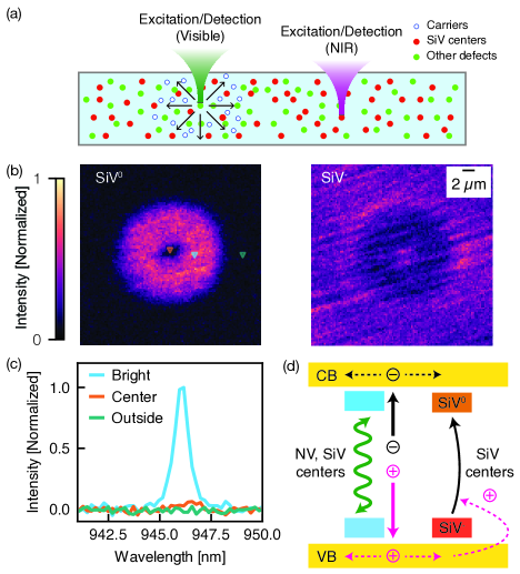
The source of itinerant carriers can be impurities and defects such as P1 centers, vacancies, and divacancies, or from color centers such as SiV and NV centers [14, 15, 16]. We hypothesize that the observed charge state conversion relies on the charge cycling of color centers (Fig. 1(d)), where the simultaneous ionization and recombination processes keep the centers photoactive and generate a continuous flow of itinerant holes and electrons. By contrast, photoionization of a P1 center only produces a single electron and then converts the P1 center to a photo-inactive state. Carriers that are injected into the conduction band and valence band can diffuse away and get captured by defects in the vicinity. We observe that in our sample (Fig. 1(b)), the SiV- centers capture the free holes to form SiV0 centers while the opposite process (SiV0 centers capturing free electrons) is less likely to happen. This preferential hole capture is consistent with recent observations in NV centers where Coulomb attraction makes the hole capture process for NV- dominant over the electron capture process for NV0 [14, 17], and the large hole capture cross section may aris from Rydberg-like bound exciton states in SiV0 [23].
The charge state distribution after a laser raster scan results from the interplay between competing non-local and local effects [15, 16]. Utilizing both non-local SiV0 generation and local SiV- preparation from 532 nm illumination, we can prepare large areas of SiV centers into desired charge states on-demand. We perform 532 nm initialization scans followed by readout of SiV0 using weak 857 nm excitation. Under high power 532 nm initialization scans, the charge state of SiV is dominated by carrier diffusion and capture, giving rise to higher SiV0 population (Fig. 2(a)). Under low power 532 nm initialization scans, the charge state of SiV is dominated by local ionization processes, forming SiV- centers (Fig. 2(b)). These nonequilibrium SiV0 centers are long-lived in the dark, with no observable decay up to 30 minutes (Fig. S2 [21]). We note that SiV0 centers prepared using high power raster scans display lower intensity compared to SiV0 centers generated via only hole capture (Fig. 2(a)). This contrast is limited by the non-negligible local ionization dynamics, and demonstrates that higher charge state initialization fidelities can be achieved with itinerant carrier capture.
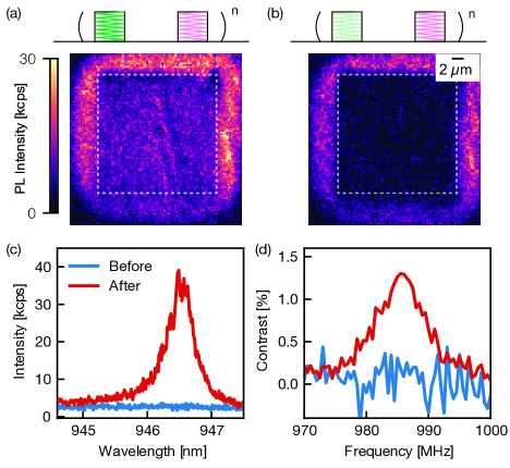
The on-demand generation of SiV0 centers stabilizes their charge state in a nonequilibrium configuration. We probe their optical and spin properties to test their stability and utility for quantum applications under illumination. Photoluminescence excitation (PLE) spectroscopy reveals a strong signal at the SiV0 zero-phonon line (946 nm) after optical preparation (Fig. 2(c)), as well as an ODMR signal at the zero field splitting (986 MHz) (Fig. 2(d)), while there was no signal before optical illumination. The observed optical and spin transitions of nonequilibrium SiV0 centers are consistent with previous observations [19, 23], demonstrating that charge state stabilization with photoactivated itinerant carriers is an promising alternative approach for generating SiV0.
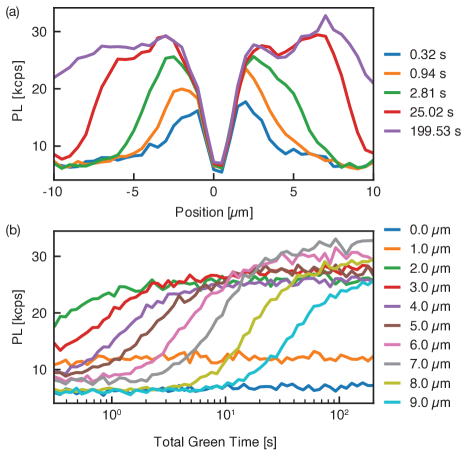
We also probe carrier diffusion dynamics and SiV0 formation by taking temporal snapshots of the spatial distribution of SiV0. The 532 nm illumination and NIR readout are interleaved to measure the time-dependent evolution of SiV0 distribution in a single experimental run. We observe that the size of the torus grows exponentially over time, and the SiV0 intensity saturates at similar levels at long times for different spatial positions (Fig. 3), indicating the establishment of a steady-state population. We estimate the charge state initialization to be around 40% based on the depletion of SiV-. We note that the growth rate of the torus appears slower than a diffusion process described by Brownian motion (Fig. S3 and Fig. S4 [21]), which could be related to the high concentration of SiV centers in our sample and space-charge effects [24].
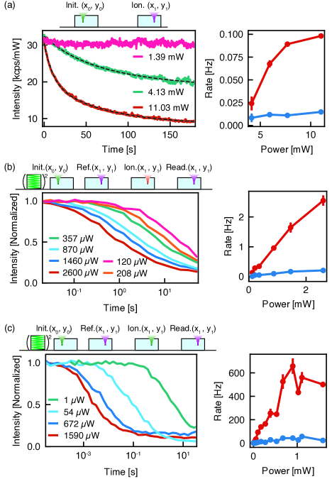
In order to probe the stability of these nonequilibrium SiV0 centers, we study their ionization dynamics under different excitation wavelengths. For many applications, the relevant excitation wavelength is near the zero phonon line. Using 857 nm excitation, which is below the ionization threshold (1.5 eV [25]), we observe that the SiV0 fluorescence decays over long time scales, with the decay undetectable over minutes for 1.39 mW excitation power (Fig. 4(a)). The long-term stability shows that SiV0 centers prepared by transient carrier doping can be stable during optical addressing, over time scales longer than their spin coherence times [19]. The decay exhibits two characteristic time scales, which has been previously observed in NV and SiV- centers [7, 15]. We observe that the faster decay rate increases with power and then saturates at high powers, while the slower rate shows a much weaker power dependence and also appears saturated at higher powers. This power dependence is inconsistent with two-photon ionization of holes to the valence band. One possible microscopic mechanism for the observed saturation is that local charge traps may facilitate ionization, and once the traps are filled, the ionization rate saturates (Fig. S5(b) [21]).
We use 637 nm excitation to study the ionization dynamics above the SiV0 ionization threshold. We observe a decay timescale on the order of seconds (Fig. 4(b)). The rate scales linearly with power, consistent with a single-photon ionization process, which is expected for excitation above the ionization threshold.
We also use 532 nm excitation to probe the interplay between the ionization of SiV0 centers and the charge dynamics of the coexisting NV centers. For 532 nm, the ionization rate is much faster, reaching 500 Hz with 1 mW excitation power (Fig. 4(c)). The drastically different ionization behavior of SiV0 under 637 nm and 532 nm excitation implies that NV centers play a key role. Specifically, they can act as traps for the transiently generated holes (Fig. S5(b) [21]). Under 532 nm excitation, NV centers are dynamically initialized into NV-, and thus can capture holes arising from SiV0 ionization [26]. Under 637 nm excitation, NV- centers are ionized into NV0. In this case, the NV centers cannot charge cycle and are unable to affect the dynamics of SiV0. Above 1 mW, the ionization rate saturates. The origin of this saturation is subject to further study, but we note that photoionization of P1 centers under 532 nm can produce a local space-charge potential [24], which may prevent the hole diffusion and limit the SiV0 ionization [21].
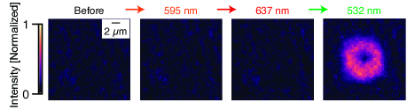
Finally, we study the origin of photoactivated carriers in our sample by probing the SiV0 distribution in the same region after laser illumination at different wavelengths. Under the same excitation power and illumination time, we only observed appreciable SiV0 formation with 532 nm but not with 595 nm and 637 nm (Fig. 5). For efficient generation of itinerant carriers, the excitation has to enable charge cycling to produce a continuous flow of holes and electrons. For example, NV centers are capable of continuously generating carriers under 532 nm illumination but not under 632 nm illumination because charge cycling is only possible for wavelengths below the zero-phonon line of NV0 at 575 nm [17]. With the observed sharp transition between 532 nm and 595 nm and the high concentration of NV centers in our sample, we conclude that NV centers play a major role in the observed generation of nonequilibrium SiV0. We note that we observe a much weaker effect of SiV0 formation under 637 nm excitation at much higher power for an extended duration (Fig. S7 [21]), which may be related to optical excitation and charge cycling of SiV centers [16].
We note that recent experiments have reported different charge dynamics for SiV centers. Specifically, SiV- centers were observed to enter a dark state under 532 nm illumination or to be converted from a dark state via carrier capture. The nature of this dark state was assigned to either SiV0 or SiV2- [15, 16]. In these prior works, the assignment was based on an indirect probe of the dark state where only SiV- centers were measured. With the ability to probe both SiV0 and SiV- centers, we can assess the charge dynamics more directly. In the sample studied in this manuscript, SiV- is dominant in the dark, stable under 532 nm excitation, and can be converted to SiV0 via hole capture. At the same time, in a different sample, we observed signatures of SiV2- in the dark, and sequential formation of SiV0 centers via double hole capture (Fig. S11 [21]). We observe that the hole capture photodoping effect of SiV centers is robust across different samples, while the SiV center charge state under direct illumination and the dark state without illumination can be sample dependent, likely due to the different charge environments arising from different impurity concentrations.
In conclusion, we have demonstrated that photoactivated itinerant carriers can be used to stabilize a highly nonequilibrium charge distribution, which opens the possibility of using nonequilibrium charge states of color centers in quantum devices. Specifically, this approach does not rely on complicated optical pulse sequence design or careful bulk substrate engineering. One possible direction is to use photoactivated carriers to stablize single SiV0 centers (Fig. S12 and Fig. S13 [21]) and study charge transport and carrier capture in the presence of an electric field, as has been shown for single NV centers [17]. Furthermore, our approach for creating nonequilibrium charge distributions should also be applicable to a broader range of diamond color centers. For example, the neutral charge state species of other group IV vacancy centers in diamond remain elusive [27, 28], and itinerant carrier capture may allow for their stabilization and observation.
Acknowledgements.
We thank S. Kolkowitz, C. Meriles, and A. Lozovoi for fruitful discussions, as well as L. Rodgers, and Z. Yuan for comments on the manuscript. The study of nonlocal charge state effects was primarily supported by the U.S. Department of Energy, Office of Science, National Quantum Information Science Research Centers, Co-design Center for Quantum Advantage (C2QA) under contract number DE-SC0012704. The confocal microscope and experimental apparatus was built using support from the National Science Foundation through the Princeton Center for Complex Materials, a Materials Research Science and Engineering Center (Grant No. DMR-1420541), and SiV0 charge state spectroscopy was developed with support from the Air Force Office of Scientific Research under Grant No. FA9550-17-0158.References
- Gao et al. [2015] W. B. Gao, A. Imamoglu, H. Bernien, and R. Hanson, Coherent manipulation, measurement and entanglement of individual solid-state spins using optical fields, Nature Photonics 9, 363 (2015).
- Atatüre et al. [2018] M. Atatüre, D. Englund, N. Vamivakas, S.-Y. Lee, and J. Wrachtrup, Material platforms for spin-based photonic quantum technologies, Nature Reviews Materials 3, 38 (2018).
- Awschalom et al. [2018] D. D. Awschalom, R. Hanson, J. Wrachtrup, and B. B. Zhou, Quantum technologies with optically interfaced solid-state spins, Nature Photonics 12, 516 (2018).
- Doi et al. [2016] Y. Doi, T. Fukui, H. Kato, T. Makino, S. Yamasaki, T. Tashima, H. Morishita, S. Miwa, F. Jelezko, Y. Suzuki, and N. Mizuochi, Pure negatively charged state of the nv center in -type diamond, Phys. Rev. B 93, 081203 (2016).
- Lühmann et al. [2019] T. Lühmann, R. John, R. Wunderlich, J. Meijer, and S. Pezzagna, Coulomb-driven single defect engineering for scalable qubits and spin sensors in diamond, Nature Communications 10, 4956 (2019).
- Aslam et al. [2013] N. Aslam, G. Waldherr, P. Neumann, F. Jelezko, and J. Wrachtrup, Photo-induced ionization dynamics of the nitrogen vacancy defect in diamond investigated by single-shot charge state detection, New Journal of Physics 15, 013064 (2013).
- Dhomkar et al. [2018a] S. Dhomkar, H. Jayakumar, P. R. Zangara, and C. A. Meriles, Charge Dynamics in near-Surface, Variable-Density Ensembles of Nitrogen-Vacancy Centers in Diamond, Nano Letters 18, 4046 (2018a).
- Yuan et al. [2020] Z. Yuan, M. Fitzpatrick, L. V. H. Rodgers, S. Sangtawesin, S. Srinivasan, and N. P. de Leon, Charge state dynamics and optically detected electron spin resonance contrast of shallow nitrogen-vacancy centers in diamond, Phys. Rev. Research 2, 033263 (2020).
- Beha et al. [2012] K. Beha, A. Batalov, N. B. Manson, R. Bratschitsch, and A. Leitenstorfer, Optimum photoluminescence excitation and recharging cycle of single nitrogen-vacancy centers in ultrapure diamond, Phys. Rev. Lett. 109, 097404 (2012).
- Siyushev et al. [2013] P. Siyushev, H. Pinto, M. Vörös, A. Gali, F. Jelezko, and J. Wrachtrup, Optically controlled switching of the charge state of a single nitrogen-vacancy center in diamond at cryogenic temperatures, Phys. Rev. Lett. 110, 167402 (2013).
- Sipahigil et al. [2016] A. Sipahigil, R. E. Evans, D. D. Sukachev, M. J. Burek, J. Borregaard, M. K. Bhaskar, C. T. Nguyen, J. L. Pacheco, H. A. Atikian, C. Meuwly, R. M. Camacho, F. Jelezko, E. Bielejec, H. Park, M. Lončar, and M. D. Lukin, An integrated diamond nanophotonics platform for quantum-optical networks, Science 354, 847 (2016).
- Waldherr et al. [2011] G. Waldherr, J. Beck, M. Steiner, P. Neumann, A. Gali, T. Frauenheim, F. Jelezko, and J. Wrachtrup, Dark States of Single Nitrogen-Vacancy Centers in Diamond Unraveled by Single Shot NMR, Phys. Rev. Lett. 106, 157601 (2011).
- Bluvstein et al. [2019] D. Bluvstein, Z. Zhang, and A. C. B. Jayich, Identifying and mitigating charge instabilities in shallow diamond nitrogen-vacancy centers, Phys. Rev. Lett. 122, 076101 (2019).
- Jayakumar et al. [2016] H. Jayakumar, J. Henshaw, S. Dhomkar, D. Pagliero, A. Laraoui, N. B. Manson, R. Albu, M. W. Doherty, and C. A. Meriles, Optical patterning of trapped charge in nitrogen-doped diamond, Nature Communications 7, 12660 (2016).
- Dhomkar et al. [2018b] S. Dhomkar, P. R. Zangara, J. Henshaw, and C. A. Meriles, On-demand generation of neutral and negatively charged silicon-vacancy centers in diamond, Phys. Rev. Lett. 120, 117401 (2018b).
- Gardill et al. [2021] A. Gardill, I. Kemeny, M. C. Cambria, Y. Li, H. T. Dinani, A. Norambuena, J. R. Maze, V. Lordi, and S. Kolkowitz, Probing Charge Dynamics in Diamond with an Individual Color Center, Nano Letters 21, 6960 (2021).
- Lozovoi et al. [2021] A. Lozovoi, H. Jayakumar, D. Daw, G. Vizkelethy, E. Bielejec, M. W. Doherty, J. Flick, and C. A. Meriles, Optical activation and detection of charge transport between individual colour centres in diamond, Nature Electronics 4, 717 (2021).
- Gali and Maze [2013] A. Gali and J. R. Maze, Ab initio study of the split silicon-vacancy defect in diamond: Electronic structure and related properties, Phys. Rev. B 88, 235205 (2013).
- Rose et al. [2018] B. C. Rose, D. Huang, Z.-H. Zhang, P. Stevenson, A. M. Tyryshkin, S. Sangtawesin, S. Srinivasan, L. Loudin, M. L. Markham, A. M. Edmonds, D. J. Twitchen, S. A. Lyon, and N. P. de Leon, Observation of an environmentally insensitive solid-state spin defect in diamond, Science 361, 60 (2018).
- Zhang et al. [2022] Z.-H. Zhang, J. A. Zuber, L. V. H. Rodgers, X. Gui, P. Stevenson, M. Li, M. Batzer, M. l. Grimau, B. Shields, A. M. Edmonds, N. Palmer, M. L. Markham, R. J. Cava, P. Maletinsky, and N. P. de Leon, Neutral silicon vacancy centers in undoped diamond via surface control, arXiv 10.48550/ARXIV.2206.13698 (2022).
- [21] See Supplemental Material for methods and additional characterization data.
- Edmonds et al. [2012] A. M. Edmonds, U. F. S. D’Haenens-Johansson, R. J. Cruddace, M. E. Newton, K.-M. C. Fu, C. Santori, R. G. Beausoleil, D. J. Twitchen, and M. L. Markham, Production of oriented nitrogen-vacancy color centers in synthetic diamond, Phys. Rev. B 86, 035201 (2012).
- Zhang et al. [2020] Z.-H. Zhang, P. Stevenson, G. m. H. Thiering, B. C. Rose, D. Huang, A. M. Edmonds, M. L. Markham, S. A. Lyon, A. Gali, and N. P. de Leon, Optically detected magnetic resonance in neutral silicon vacancy centers in diamond via bound exciton states, Phys. Rev. Lett. 125, 237402 (2020).
- Lozovoi et al. [2020] A. Lozovoi, H. Jayakumar, D. Daw, A. Lakra, and C. A. Meriles, Probing metastable space-charge potentials in a wide band gap semiconductor, Phys. Rev. Lett. 125, 256602 (2020).
- Allers and Collins [1995] L. Allers and A. T. Collins, Photoconductive spectroscopy of diamond grown by chemical vapor deposition, Journal of Applied Physics 77, 3879 (1995).
- Nicolas et al. [2019] L. Nicolas, T. Delord, P. Huillery, C. Pellet-Mary, and G. Hétet, Sub-ghz linewidth ensembles of siv centers in a diamond nanopyramid revealed by charge state conversion, ACS Photonics 6, 2413 (2019).
- Thiering and Gali [2018] G. Thiering and A. Gali, Ab initio magneto-optical spectrum of group-iv vacancy color centers in diamond, Phys. Rev. X 8, 021063 (2018).
- Thiering and Gali [2019] G. Thiering and A. Gali, The product Jahn–Teller effect in the neutral group-IV vacancy quantum bits in diamond, npj Computational Materials 5, 18 (2019).