2021
[1]\fnmPrachi \surVenkat
[1]\orgdivKPSI, \orgnameNational Institutes for Quantum Science and Technology, \orgaddress\street8-1-7, Umemidai, \cityKizugawa, \postcode619-0125, \stateKyoto, \countryJapan 2]\orgdivPhoton Science Center, \orgnameThe University of Tokyo, \orgaddress\street7-3-1, Hongo, \cityBunkyo-ku, \postcode111-8656, \stateTokyo, \countryJapan
Wavelength dependence of laser-induced excitation dynamics in silicon
Abstract
Effect of laser wavelength on the carrier-phonon dynamics and damage threshold of silicon is studied numerically. Laser excitation dynamics in silicon is studied using Three-Temperature Model (3TM). We consider the evolution of electron, hole, and lattice temperatures separately and including band-gap re-normalization effect on optical properties of silicon. Finite Difference Time Domain method is used to model the laser field. Damage threshold calculated using the 3TM is in reasonable agreement with the experiments. Our results indicate that the competition of inter-band excitation, plasma heating, and electron-phonon relaxation process defines the damage threshold for various wavelengths and pulse durations.
keywords:
Laser processing, Damage threshold, Wavelength dependence, Numerical modeling1 Introduction
Laser processing studies of semiconductors like silicon are crucial for the practical applications in the field of nano-fabrication Gattass2008 ; Stoian-2020 . Interaction of intense, femto-second pulses with a target can lead to high resolution in transfer of energy, with minimum damage to the surrounding area Sugioka2014 . Laser excitation of semiconductors involves complex physics of photo-absorption, impact ionization, re-combination and re-distribution of energy. It is the dynamics of the interaction that ultimately leads to structural changes through thermal and non-thermal effects.
Numerical modeling allows us to study the dynamics of laser excitation in silicon in detail. The onset and nature of damage can be better understood by taking into account all the processes occurring within the lattice and their respective time frames. Theoretical modeling of such interactions usually involves the use of Two-Temperature model (TTM), which is a widely implemented approach to study the evolution of electron and lattice dynamics during laser excitation. TTM was initially developed to study the dynamics in metals Anisimov1974 and then extended to study excitation in semiconductors Agassi-1984 ; VanDriel-1987 . More recently, a self-consistent density-dependent TTM (nTTM) has been implemented to study the evolution of carrier densities, temperatures and lattice temperature in the material Chen-2005 .
The dynamics following the laser excitation involves a progression of carrier excitation, relaxation and electron-hole-phonon dynamics. The electron and hole relaxation in conduction and valence bands is observed to be faster than relaxation of the system as a whole (Zurch2017, ). Electron-hole scattering frequency decreases significantly with the increase in electron temperature Terashige-2015 . The calculations presented using first-principles numerical simulation show that electron and hole energies evolve differently, depending on the band structure. The energy difference between electrons and holes suggests that quasi-temperatures are different in the conduction band (CB) and valence band (VB) (Otobe-2019, ). Also, the decreased electron-hole scattering frequency indicates that it is important to take quasi-temperatures of electrons and holes into consideration. A modified nTTM treating the evolution of quasi-temperatures in CB, VB and lattice (3TM) has been proposed in our previous work 3TM-2022 .
Carrier density Density of valence electrons Reduced quasi Fermi-level Carrier charge; ; Electron(hole) mobility Electron(hole) temperature Lattice temperature Boltzmann Constant Diffusion coefficient Electric field due to e-h separation Charge current Energy current Single photon absorption coefficient Free carrier absorption coefficient 2-photon absorption coefficient Real part of susceptibility () Laser wavelength Pulse duration in FWHM
The 3TM is modeled to consider three sub-systems, electrons, holes and lattice, and their temperatures are calculated separately. The carrier densities are also calculated distinctively for electrons and holes. We treat the dynamics of laser field by solving one-dimensional Maxwell’s equations, using the Finite Difference Time Domain (FDTD) approach. The effect of band re-normalization on the optical properties of silicon is also included Sokol-2000 . We use Drude model to calculate the complex dielectric function, and thereby include the effect of free carrier response in photo-absorption Silaeva_2012 .
Lattice thermal conductivity VanDriel-1987 W/(cm K) Lattice heat capacity VanDriel-1987 J/cm3 Electron DoS effective mass Lipp-2014 ; BARBER-1967 Hole DoS effective mass Lipp-2014 ; BARBER-1967 Electron mobility Meyer-1980 ; Lipp-2014 m2/Vs Hole mobility Meyer-1980 ; Lipp-2014 m2/Vs Auger recombination coefficient Silaeva_2012 ; Dziewior-1977 cm6/s Auger recombination coefficient Silaeva_2012 ; Dziewior-1977 cm6/s Impact ionization coefficient VanDriel-1987 Change in band gap eV Sokol-2000 Band gap function eV e-ph relaxation time Yoffa-1981 ; Agassi-1984 ; VanDriel-1987 ; sjodin-1998 ; Harb-2006 e-ph relaxation time constant sjodin-1998 ; Chen-2005 240 fs
In order to understand and define damage in silicon, we can assume several processes that may be responsible for causing permanent structural changes. In our previous study, we have compared the calculated thresholds for possible damage mechanisms with the experimental damage thresholds to understand the nature of damage in silicon and the interaction conditions affecting it 3TM-2022 . Changing the wavelength of incident pulse can lead to significant changes in the dynamics of the interaction Gallais-2015 . Since the photon energy changes, the excitation mechanisms involving single- and two- photon absorption may be affected, in turn affecting the carrier density and temperatures. Apart from photon energy, the penetration depth for single- and two-photon absorption in silicon changes with the wavelength and can lead to different degrees of damage and structural changes.
In this paper, we study the interaction of laser pulse of different wavelengths with a silicon film of fixed thickness and the effect on damage threshold. The paper is organized as follows: Section 2 includes the details of the numerical model, sec. 3 consists of the results and discussion and sec. 4 summarizes the study.
2 Numerical Scheme
Laser irradiation of Silicon target leads to excitation of the electrons from valence band to conduction band and a complex interplay of carrier and lattice dynamics, ultimately leading to thermal equilibrium. Single- and two-photon absorption, impact ionization and Auger recombination occur during laser excitation of silicon and affect the temporal evolution of transient carrier densities. Carrier-phonon interaction is responsible for the re-distribution of energy within the carrier and lattice system.
The present model is similar to nTTM Chen-2005 , with some key differences. Firstly, the system is considered to consist of three sub-systems viz., electrons, holes and the lattice. The electron and hole densities are calculated separately, as are the electron, hole and lattice temperatures. Also, the effect of band structure re-normalization is taken into account while calculating the dielectric function and single- and two-photon absorption coefficients.The model is explained in detail in Ref. 3TM-2022 . Tables 1 and 2 list the notation and values for various parameters and variables used.
The time-evolution of electron and hole densities, and is described as:
| (1) |
where is the laser frequency and is the single-photon absorption coefficient for transition from VB to CB (Green2008, ). is the two-photon absorption coefficient for which we use the DFT calculation when Murayama-1995 , where is the optical gap. Around the band gap energy we employ interpolation to the model described in Ref.Alan2007 ; Garcia_2006 ; Furey-2021 . is the Auger re-combination coefficient (Silaeva_2012, ) and is the impact ionization coefficient (Chen-2005, ). Equation 1 also includes the effect of spatial charge distribution and the associated electric field, and and are the charge current, diffusion coefficient and the electric field induced by the electron–hole separation, respectively 3TM-2022 .
The total dielectric function along with the effect of band structure re-normalization (Sokol-2000, ) is expressed by
| (2) |
where is the density of valence electrons. and are nearly the same due to the effect of and can be approximated at . is the innate dielectric function, represents the band re-normalization by carrier density, and is the complex dielectric function calculated from Drude model 3TM-2022 . The total one-photon absorption coefficient including free-carrier absorption is calculated using the complex dielectric function 3TM-2022 . The temperature dependent optical parameters of silicon are referred to from Ref.(Green2008, ).
The temperature evolution of the electron, hole and lattice sub-systems is calculated as:
| (3) |
| (4) |
The third and fourth terms in Eq. (3) account for the loss of energy due to electron-lattice interaction and energy current. The last two terms on right hand side include the changes in carrier density and band gap energy. Here, and is the Fermi integral. The heat capacities are calculated from the carrier densities and temperatures. is calculated following the empirical model, where the term for carrier temperature is replaced by terms for electron and hole temperatures, as described in Eq. (4). Here, is the thermal conductivity 3TM-2022 .
The propagation of the laser pulse is described by solving the Maxwell’s equations using FDTD method. Mur’s absorbing boundary condition is employed to prevent reflection from the boundary (Mur-1981, ). Also, the electric field is considered to be complex for the calculation of laser intensity, so as to ensure a non-zero field at all points in time and space. Assuming a one-dimensional system, the electric field is:
| (5) |
Here includes Gaussian envelope defining the shape of the pulse as , where , being the FWHM pulse duration.
| (6) |
where is the laser intensity. Evaluation of charge current induced by the laser field is a crucial part of the module. We calculate the current with and without excitation i.e., for photo-absorption and dielectric response. For dielectric response, is calculated as:
| (7) |
where is the vector potential, is the polarization and is the real part of susceptibility (). The Maxwell’s equation thus, becomes
| (8) |
where
| (9) |
is the current associated with photo-absorption.
3 Results and discussion
We study the interaction of laser pulse of wavelengths () 515 nm ( eV), 625 nm ( eV) and 775 nm ( eV) with silicon film of thickness 60 m. Since the penetration depth differs depending on the wavelength, we choose a film thickness where the reflection from the rear surface does not cause interference with the EM-field within the film. The corresponding penetration depths for single-photon absorption () in case of 515 nm, 625 nm and 775 nm are m, m and m respectively Green-1995 .
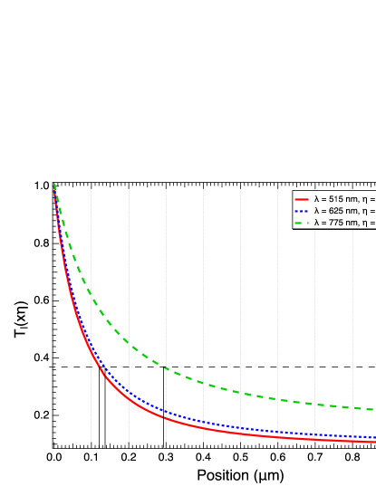
Figure 1 shows the lattice temperature gradient within the silicon film at the last time step of the simulation for different . The pulse duration and incident fluence are 350 fs and 0.18 J/cm2. The temperature is normalized by the factor of . The maximum lattice temperature on the surface of the film is given by , which decreases with the decrease in photon energy. The penetration depth for single-photon absorption is different in case of each . We also look at the evolution of lattice temperature with position and the depth at which falls to of the maximum value. This processed depth for is 0.12 m in case of 515 nm, 0.14 m for 625 nm and 0.3 m for 775 nm. The change in processed depth indicates the effect of wavelength on the dynamics, which may be due to the different photon energies, affecting the absorption mechanism and plasma response. The two-photon absorption coefficient is 37.6 cm/GW Murayama-1995 , 36.9 cm/GW Murayama-1995 and 1.9 cm/GW Alan2007 for 515 nm, 625 nm and 775 nm respectively. Both single- and two-photon absorption processes become less intense with the increasing wavelength. for the three wavelengths is 0.027 GW/cm, 0.027 GW/cm and 0.526 GW/cm, respectively. The processed depth increases with increasing , which seems inconsistent with the decrease in and . This indicates that while photon absorption becomes less intense with increase in from 515 nm to 775 nm, plasma heating may observe an increase. The absorption of energy by the plasma can be considered responsible for the increased processed depth in case of 775 nm.
The variation in the dynamics and processed depth with would also manifest as change in the damage threshold, and has been observed in experimental studies as well Sokol-2000 ; Pronko-1998 ; Bonse-2002 ; Smirnov2018 ; Gallais-2015 . The effect of variation can also potentially help control the processing depth in the target. The damage or permanent structural alterations in the sample can be studied in different ways Allen-2003 ; Bonse-2002 ; Izawa_2006 ; Mirza2016 ; Thorstensen-2012 . The possible processes for damage and the calculation of their threshold has been discussed in detail in our previous work 3TM-2022 . We now consider three possible processes during the laser excitation of silicon, that may be responsible for causing damage.
Thermal melting can be considered significant in causing damage in the silicon lattice. The threshold () can be calculated for the onset of melting as lattice temperature reaches melting point of 1687 K (partial melting), or when bond configuration changes to tetrahedral after absorption of the total latent heat from the carriers (complete melting) Korfiatis-2007 . The two different thresholds for melting lead to different understanding of the onset of damage. The bond-breaking energy can also be considered as a reasonable candidate for the damage threshold Sato-2014 . Threshold for breaking of bonds () is calculated as the fluence at which energy per atom reaches 2.3 eV i.e., half the cohesive energy of a silicon crystal Lutrus-1993 . Emission of electrons from the surface into vacuum is also crucial in studying damage mechanisms. When the electron temperature is high, electron emission (e-emission) from the surface into the vacuum causes impulsive Coulomb force within the lattice. This force tends to de-stabilize the lattice structure, and in extreme cases causes Coulomb explosion Roeterdink-2003 . The photon energy in the three cases being studied in this work is much lower than the work function of silicon (4.65 eV), therefore photo-emission by single- and two-photon absorption is not possible. The Fermi-Dirac distribution suggests e-emission is caused as a result of thermal effects. We define the e-emission threshold () as eV. It may be noted that this assumption considers e-emission as the mere trigger for Coulomb forces that may be responsible for the actual damage. A comparison of the calculated thresholds with experimental data from Allenspacher et.al in our previous study showed that e-emission threshold coincided quite well with the damage threshold for longer 3TM-2022 .
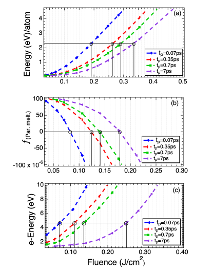
Figure 2 shows the plots for (a) energy per atom, (b) function to calculate the onset of melting () Korfiatis-2007 and (c) electron energy for the case of 625 nm and different . The threshold for each process is determined from the plot as the fluence at which the plot reaches the threshold condition. is marked on each plot where the maximum energy per atom is 2.3 eV. In case of partial melting, is marked where the function f becomes zero. In case of e-emission, the fluence at which the average energy of electrons is 4.65 eV, is marked as . The thresholds for the three processes obtained in this manner are then plotted with pulse duration () in fig. 3.
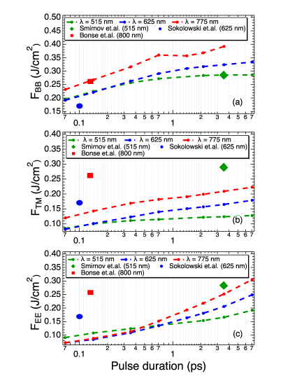
Figure 3 shows the calculated , and for pulses of three different wavelengths. The calculated thresholds are plotted for different . Since the lattice temperature evolution is similar for 515 nm and 625 nm as shown in fig. 1, and are nearly the same, as long as ps. As increases well beyond the e-ph interaction time and the relaxation time for electron-phonon dynamics,the dynamics and energy transition get affected, and the thresholds are not the same for the three cases of .
In fig. 3 (c), for different wavelengths show a similar trend. For 775 nm pulse, the e-emission threshold is comparable with the thresholds for shorter , for ps. For longer , the thresholds become markedly different for the three cases. The dependence of threshold on is increased 3TM-2022 and combined with the difference in photon energy, the e-emission threshold for longer pulses is different for varying . It can also be observed that is lower for the lower photon energies of 1.6 and 1.98 eV. This may be a result of the change in plasma frequency with increasing wavelength. The resonant absorption depends on the plasma frequency and critical density for a particular case of and this may be responsible for the lower e-emission threshold for longer wavelength.
On comparing the calculated values of , and , it was seen that coincided most with the experimental data. Table 3 shows the experimental threshold for different cases of and the calculated threshold for breaking of bonds. The experimental data is also indicated in fig. 3. The damage threshold is defined differently in the experimental studies, making the comparison of calculated and experimental data for different studies challenging.
(nm) (ps) Fexp. FBB 515 Smirnov2018 3.5 0.286 0.286 0.0 625 Sokol-2000 0.1 0.17 0.21 23.5 775 Bonse-2002 0.13 0.26 0.264 1.5
In case of 625nm, the experiment observed the melting threshold. The calculated threshold for melting as well as breaking of bonds showed error Sokol-1995 . For 775nm, the experimental threshold was calculated by plotting the diameter of the damaged spot with the incident fluence and extrapolating the plot to obtain the fluence when diameter became zero Bonse-2002 . The agreement of experimental data with breaking of bonds may be due to the definition of threshold, which is defined when the damaged spot appears. The experiments where damaged area is considered means that the damage probability is 100 . On the other hand, in the experimental study by Allenspacher et.al., the damage threshold is determined when the damage probability is 0 Allen-2003 . Due to this difference in definitions, the experimental data in former case agrees with calculated , and in latter case it agrees with calculated and 3TM-2022 .
In case of 515 nm, the experimental data reported by Smirnov et. al consists of damage threshold over a range of pulse duration Smirnov2018 . Smirnov et. al defined the threshold from the radius of the ablation crater by considering it as a function of the natural logarithm of the energy (). Ablation threshold is where is ablation threshold and is the focal spot at 1/e of the energy density. Comparison of our calculated threshold with Smirnov et.al data showed that the calculations were in agreement with experiment for pulse duration longer than 1 ps, and the data for a particular case of ps is shown in table 3. For ps, the calculated threshold did not match the experimental threshold. For shorter pulses of ps, the experimental threshold is J/cm2, which is much higher than the calculated threshold. Smirnov et.al explain the high threshold for shorter as a result of faster ambipolar diffusion, as opposed to shorter diffusion stage and slower energy transition for longer . One possibility for the disagreement between our results and Smirnov et. al data for ps is the different definition of threshold. The morphology of the ablation spots and the conditions for their formation need to be studied in detail to calculate more accurate thresholds. For example, Moser et. al have reported that the hydrodynamic processes affect ablating spot size Moser18 .
4 Summary
We studied the interaction of laser pulses of varying wavelength with silicon film. The dynamics show a significant change with the wavelength, which in turn affects the damage threshold. While the bond breaking and thermal melting threshold for the case of 775 nm pulse are significantly higher due to low photon energy, the e-emission threshold for the three wavelengths is comparable due to the plasma response. The dependence of e-emission threshold increases when exceeds 0.4 ps, which may be due to the effect of carrier-phonon dynamics.
Our calculations indicate that the wavelength dependence is determined by the competition between inter-band transitions, plasma heating, and electron-lattice interactions. The first two are expected to have an effect for relatively short pulse duration, while the latter becomes more pronounced at longer pulse duration. The calculated threshold for breaking of bonds is observed to coincide the most with the experimental data.
The agreement of calculations with experimental data maybe also be due to the treatment of photo-absorption in our model. We calculate the single- and two-photon absorption coefficients as a spectrum, so as to include the effect of changing laser frequency. The study for longer wavelengths can also be done using this model, although the effect of three-photon absorption must be taken into account.
Acknowledgments
This research is supported by MEXT Quantum Leap Flagship Program (MEXT Q-LEAP) under Grant No. JPMXS0118067246. This research is also partially supported by JST-CREST under Grant No. JP-MJCR16N5. The numerical calculations are carried out using the computer facilities of the SGI8600 at Japan Atomic Energy Agency (JAEA).
References
- \bibcommenthead
- (1) Gattass, R.R., Mazur, E.: Femtosecond laser micromachining in transparent materials. Nat. Photonics 2(4), 219–225 (2008). https://doi.org/10.1038/nphoton.2008.47
- (2) Stoian, R., Colombier, J.-P.: Advances in ultrafast laser structuring of materials at the nanoscale. Nanophotonics 9(16), 4665–4688 (2020). https://doi.org/10.1515/nanoph-2020-0310
- (3) Sugioka, K., Cheng, Y.: Ultrafast lasers—reliable tools for advanced materials processing. Light Sci. Appl 3(4), 149–149 (2014). https://doi.org/10.1038/lsa.2014.30
- (4) Anisimov, S.I., Kapeliovich, B.L., Perel’Man, T.L.: Electron emission from metal surfaces exposed to ultrashort laser pulses. J. Exp. Theor. Phys 39, 375–377 (1974)
- (5) Agassi, D.: Phenomenological model for pisosecond‐pulse laser annealing of semiconductors. J. Appl. Phys. 55(12), 4376–4383 (1984). https://doi.org/10.1063/1.333007
- (6) van Driel, H.M.: Kinetics of high-density plasmas generated in si by 1.06- and 0.53-m picosecond laser pulses. Phys. Rev. B 35, 8166–8176 (1987). https://doi.org/10.1103/PhysRevB.35.8166
- (7) Chen, J.K., Tzou, D.Y., Beraun, J.E.: Numerical investigation of ultrashort laser damage in semiconductors. Int. J. Heat Mass Transf. 48(3), 501–509 (2005). https://doi.org/10.1016/j.ijheatmasstransfer.2004.09.015
- (8) Zürch, M., Chang, H.-T., Borja, L.J., Kraus, P.M., Cushing, S.K., Gandman, A., Kaplan, C.J., Oh, M.H., Prell, J.S., Prendergast, D., Pemmaraju, C.D., Neumark, D.M., Leone, S.R.: Direct and simultaneous observation of ultrafast electron and hole dynamics in germanium. Nat. Commun. 8(1), 15734 (2017). https://doi.org/10.1038/ncomms15734
- (9) Terashige, T., Yada, H., Matsui, Y., Miyamoto, T., Kida, N., Okamoto, H.: Temperature and carrier-density dependence of electron-hole scattering in silicon investigated by optical-pump terahertz-probe spectroscopy. Phys. Rev. B 91, 241201 (2015). https://doi.org/10.1103/PhysRevB.91.241201
- (10) Otobe, T.: Macroscopic electron-hole distribution in silicon and cubic silicon carbide by the intense femtosecond laser pulse. J. Appl. Phys. 126(20), 203101 (2019). https://doi.org/10.1063/1.5124424
- (11) Venkat, P., Otobe, T.: Three-temperature modeling of laser-induced damage process in silicon. Applied Physics Express 15(4), 041008 (2022). https://doi.org/10.35848/1882-0786/ac5edb
- (12) Sokolowski-Tinten, K., von der Linde, D.: Generation of dense electron-hole plasmas in silicon. Phys. Rev. B 61, 2643–2650 (2000). https://doi.org/10.1103/PhysRevB.61.2643
- (13) Silaeva, E.P., Vella, A., Sevelin-Radiguet, N., Martel, G., Deconihout, B., Itina, T.E.: Ultrafast laser-triggered field ion emission from semiconductor tips. New J. Phys. 14(11), 113026 (2012). https://doi.org/10.1088/1367-2630/14/11/113026
- (14) Lipp, V.P., Rethfeld, B., Garcia, M.E., Ivanov, D.S.: Atomistic-continuum modeling of short laser pulse melting of si targets. Phys. Rev. B 90, 245306 (2014). https://doi.org/10.1103/PhysRevB.90.245306
- (15) Barber, H.D.: Effective mass and intrinsic concentration in silicon. Solid-State Electronics 10(11), 1039–1051 (1967). https://doi.org/10.1016/0038-1101(67)90122-0
- (16) Meyer, J.R., Kruer, M.R., Bartoli, F.J.: Optical heating in semiconductors: Laser damage in ge, si, insb, and gaas. J. Appl. Phys. 51(10), 5513–5522 (1980). https://doi.org/10.1063/1.327469
- (17) Dziewior, J., Schmid, W.: Auger coefficients for highly doped and highly excited silicon. Appl. Phys. Lett. 31(5), 346–348 (1977). https://doi.org/10.1063/1.89694
- (18) Yoffa, E.J.: Screening of hot-carrier relaxation in highly photoexcited semiconductors. Phys. Rev. B 23, 1909–1919 (1981). https://doi.org/10.1103/PhysRevB.23.1909
- (19) Sjodin, T., Petek, H., Dai, H.-L.: Ultrafast carrier dynamics in silicon: A two-color transient reflection grating study on a surface. Phys. Rev. Lett. 81, 5664–5667 (1998). https://doi.org/10.1103/PhysRevLett.81.5664
- (20) Harb, M., Ernstorfer, R., Dartigalongue, T., Hebeisen, C.T., Jordan, R.E., Miller, R.J.D.: Carrier relaxation and lattice heating dynamics in silicon revealed by femtosecond electron diffraction. The Journal of Physical Chemistry B 110(50), 25308–25313 (2006) https://doi.org/10.1021/jp064649n. https://doi.org/10.1021/jp064649n. PMID: 17165976
- (21) Gallais, L., Douti, D.-B., Commandré, M., Batavičiūtė, G., Pupka, E., Ščiuka, M., Smalakys, L., Sirutkaitis, V., Melninkaitis, A.: Wavelength dependence of femtosecond laser-induced damage threshold of optical materials. Journal of Applied Physics 117(22), 223103 (2015) https://doi.org/10.1063/1.4922353. https://doi.org/10.1063/1.4922353
- (22) Green, M.A.: Self-consistent optical parameters of intrinsic silicon at 300k including temperature coefficients. Sol. Energy Mater. Sol. Cells 92(11), 1305–1310 (2008). https://doi.org/10.1016/j.solmat.2008.06.009
- (23) Murayama, M., Nakayama, T.: Ab initio calculations of two-photon absorption spectra in semiconductors. Phys. Rev. B 52, 4986–4997 (1995). https://doi.org/10.1103/PhysRevB.52.4986
- (24) Bristow, A.D., Rotenberg, N., van Driel, H.M.: Two-photon absorption and kerr coefficients of silicon for 850–2200nm. Appl. Phys. Lett. 90(19), 191104 (2007). https://doi.org/10.1063/1.2737359
- (25) Garcia, H., Kalyanaraman, R.: Phonon-assisted two-photon absorption in the presence of a dc-field: the nonlinear franz–keldysh effect in indirect gap semiconductors. Journal of Physics B: Atomic, Molecular and Optical Physics 39(12), 2737–2746 (2006). https://doi.org/10.1088/0953-4075/39/12/009
- (26) Furey, B.J., Barba-Barba, R.M., Carriles, R., Bernal, A., Mendoza, B.S., Downer, M.C.: Im(3) spectra of 110-cut gaas, gap, and si near the two-photon absorption band edge. J. Appl. Phys. 129(18), 183109 (2021). https://doi.org/10.1063/5.0047478
- (27) Mur, G.: Absorbing boundary conditions for the finite-difference approximation of the time-domain electromagnetic-field equations. IEEE Trans. Electromagn. Compat. EMC-23(4), 377–382 (1981). https://doi.org/10.1109/TEMC.1981.303970
- (28) Green, M.A., Keevers, M.J.: Optical properties of intrinsic silicon at 300 k. Progress in Photovoltaics 3 (1995). https://doi.org/10.1002/pip.4670030303
- (29) Pronko, P.P., VanRompay, P.A., Horvath, C., Loesel, F., Juhasz, T., Liu, X., Mourou, G.: Avalanche ionization and dielectric breakdown in silicon with ultrafast laser pulses. Phys. Rev. B 58, 2387–2390 (1998). https://doi.org/10.1103/PhysRevB.58.2387
- (30) Bonse, J., Baudach, S., Krüger, J., Kautek, W., Lenzner, M.: Femtosecond laser ablation of silicon–modification thresholds and morphology. Appl. Phys. A 74(1), 19–25 (2002). https://doi.org/10.1007/s003390100893
- (31) Smirnov, N.A., Kudryashov, S.I., Danilov, P.A., Rudenko, A.A., Ionin, A.A., Nastulyavichus, A.A.: Silicon ablation by single ultrashort laser pulses of variable width in air and water. JETP Letters 108(6), 368–373 (2018). https://doi.org/10.1134/S002136401818011X
- (32) Allenspacher, P., Huettner, B., Riede, W.: Ultrashort pulse damage of Si and Ge semiconductors, vol. 4932, pp. 358–365. SPIE, ??? (2003). International Society for Optics and Photonics. https://doi.org/10.1117/12.472053
- (33) Izawa, Y., Setuhara, Y., Hashida, M., Fujita, M., Izawa, Y.: Ablation and amorphization of crystalline si by femtosecond and picosecond laser irradiation. Jpn. J. Appl. Phys. 45(7), 5791–5794 (2006). https://doi.org/10.1143/jjap.45.5791
- (34) Mirza, I., Bulgakova, N.M., Tomáštík, J., Michálek, V., Haderka, O., Fekete, L., Mocek, T.: Ultrashort pulse laser ablation of dielectrics: Thresholds, mechanisms, role of breakdown. Sci. Rep. 6(1), 39133 (2016). https://doi.org/10.1038/srep39133
- (35) Thorstensen, J., Erik Foss, S.: Temperature dependent ablation threshold in silicon using ultrashort laser pulses. J. Appl. Phys. 112(10), 103514 (2012). https://doi.org/10.1063/1.4766380
- (36) Korfiatis, D., Thoma, K.-A., Vardaxoglou, J.: Conditions for femtosecond laser melting of silicon. J. Phys. D: Appl. Phys 40, 6803 (2007). https://doi.org/10.1088/0022-3727/40/21/047
- (37) Sato, S.A., Shinohara, Y., Otobe, T., Yabana, K.: Dielectric response of laser-excited silicon at finite electron temperature. Phys. Rev. B 90, 174303 (2014). https://doi.org/10.1103/PhysRevB.90.174303
- (38) Lutrus, C.K., Oshiro, T., Hagen, D.E., Suck Salk, S.H.: Simulation of bulk silicon crystals and si(111) surfaces with application to a study of fluorine coverage of the surfaces. Phys. Rev. B 48, 15086–15091 (1993). https://doi.org/10.1103/PhysRevB.48.15086
- (39) Roeterdink, W.G., Juurlink, L.B.F., Vaughan, O.P.H., Dura Diez, J., Bonn, M., Kleyn, A.W.: Coulomb explosion in femtosecond laser ablation of si(111). Appl. Phys. Lett. 82(23), 4190–4192 (2003). https://doi.org/10.1063/1.1580647
- (40) Sokolowski-Tinten, K., Bialkowski, J., von der Linde, D.: Ultrafast laser-induced order-disorder transitions in semiconductors. Phys. Rev. B 51, 14186–14198 (1995). https://doi.org/10.1103/PhysRevB.51.14186
- (41) Moser, R., Domke, M., Winter, J., Huber, H.P., Marowsky, G.: Single pulse femtosecond laser ablation of silicon – a comparison between experimental and simulated two-dimensional ablation profiles. Advanced Optical Technologies 7(4), 255–264 (2018). https://doi.org/10.1515/aot-2018-0013